A Voltage Multiplier Circuit Based Quadratic Boost Converter for Energy Storage Application

 ,
,  , , , ,
Abstract
:1. Introduction
- (1)
- (2)
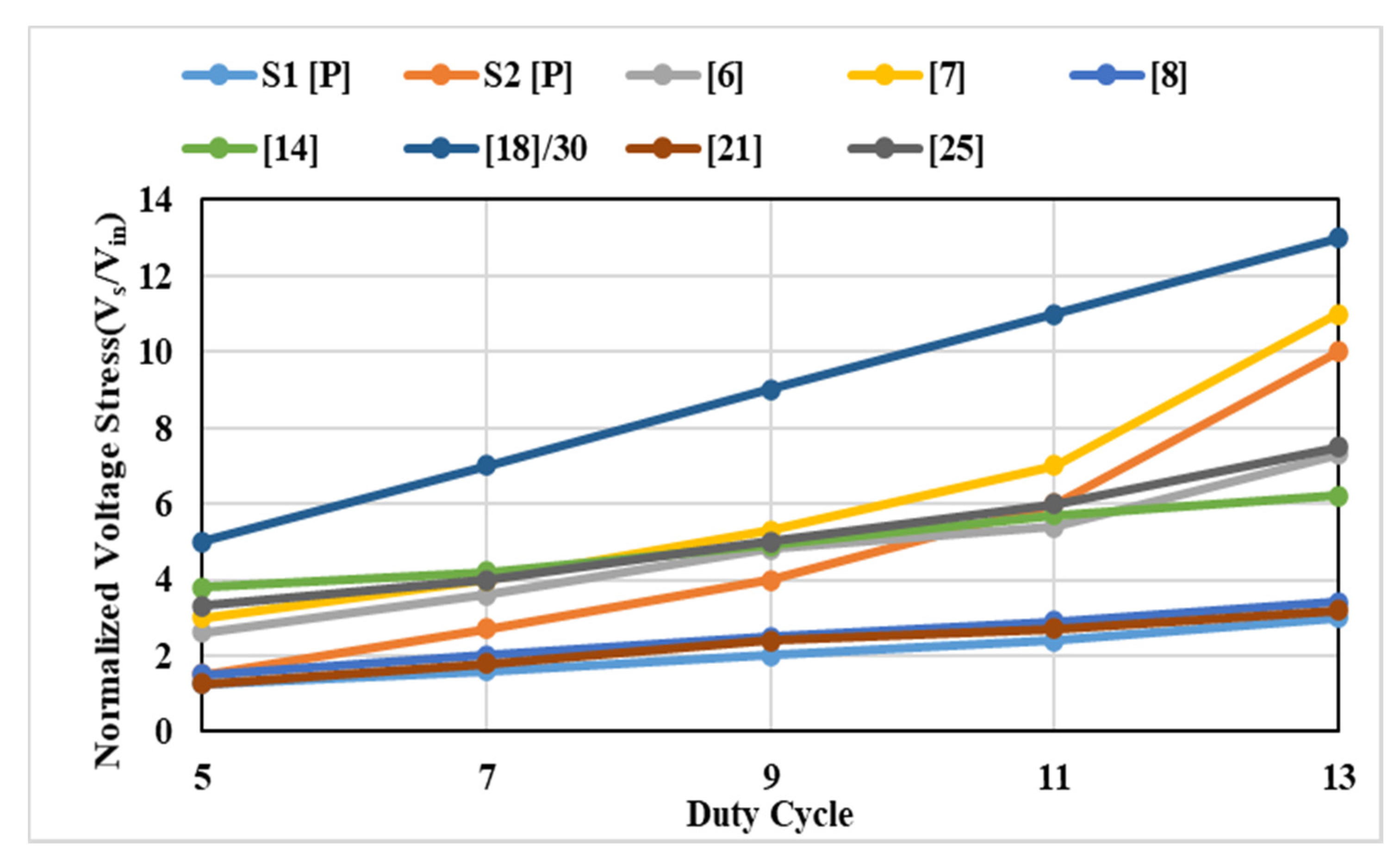
- The voltage stress across switches of the proposed converter is much less than the output voltage Vo, which is an improvement over the quadratic converters proposed in [18,30] in which the voltage stress is equal to Vo. Moreover, the diodes and capacitors also have low voltage stress, leading to the selection of low voltage rating devices and subsequently improving the converter’s efficiency.
- (3)
- To achieve this high voltage gain, the coupled inductor is not used, and hence the problem of leakage inductance and the need for a snubber circuit is avoided.
- (4)
- The input current is continuous, which is another significant advantage of the proposed topology.
- (5)
- The control of the proposed converter is easy, as two switches are turned ON and OFF simultaneously.
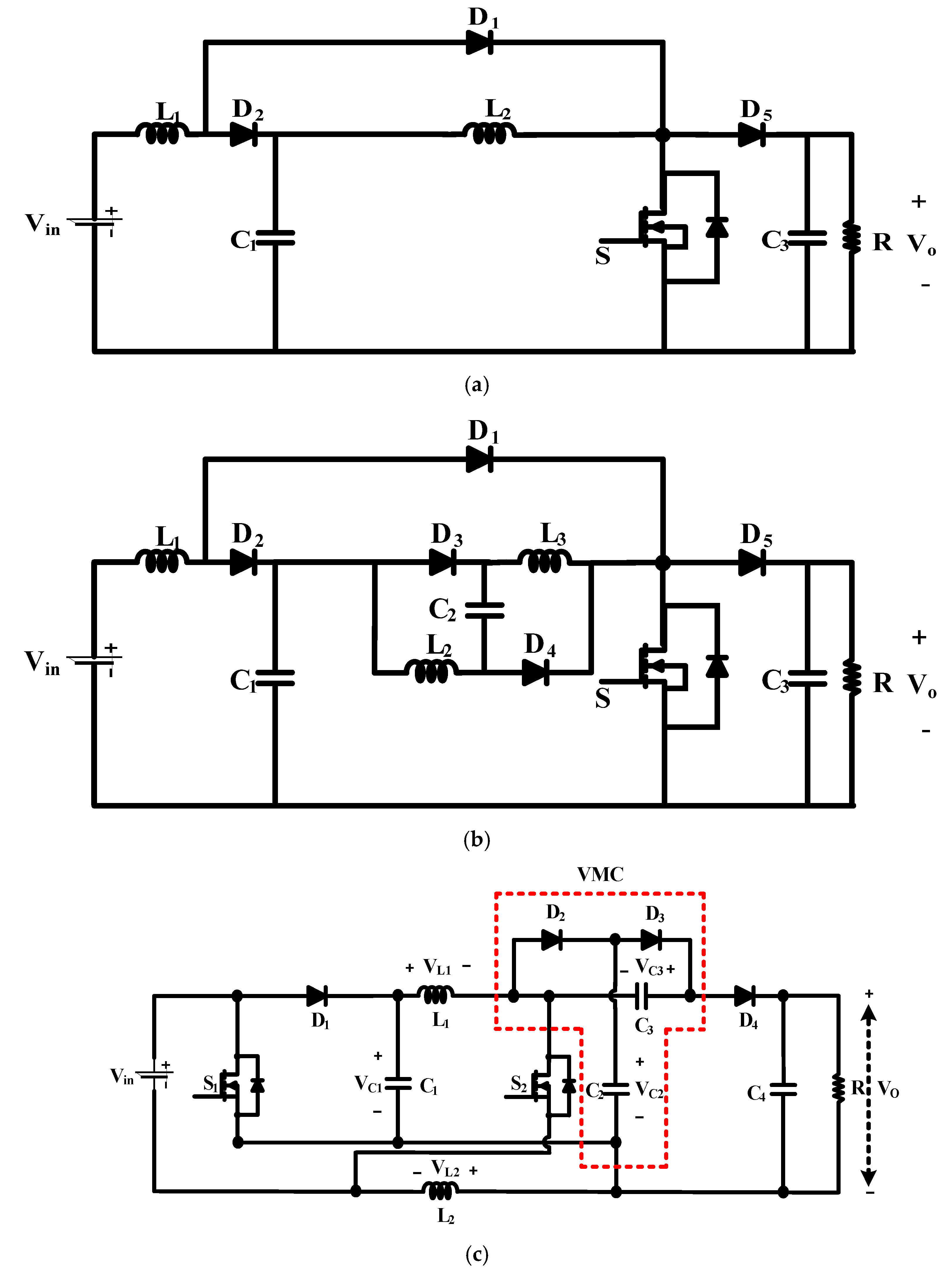
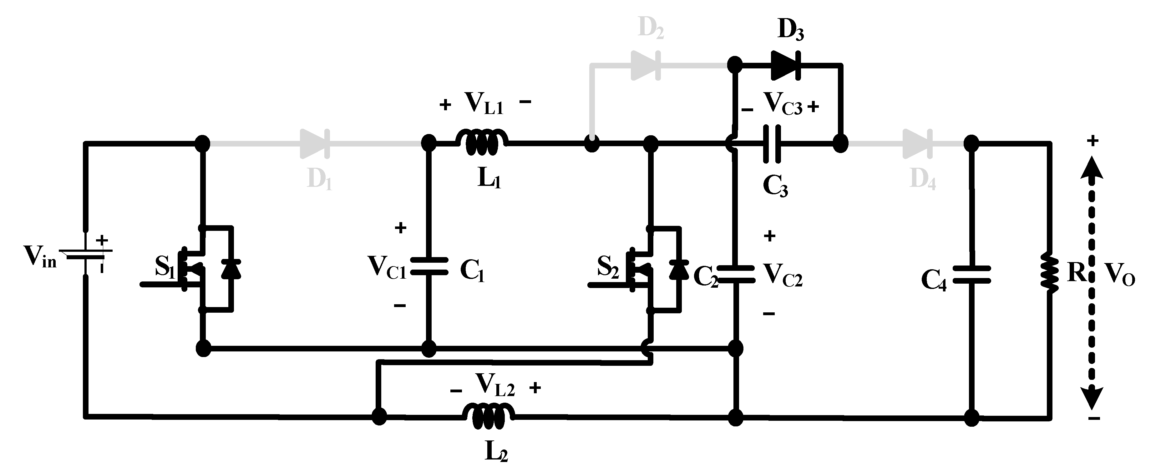
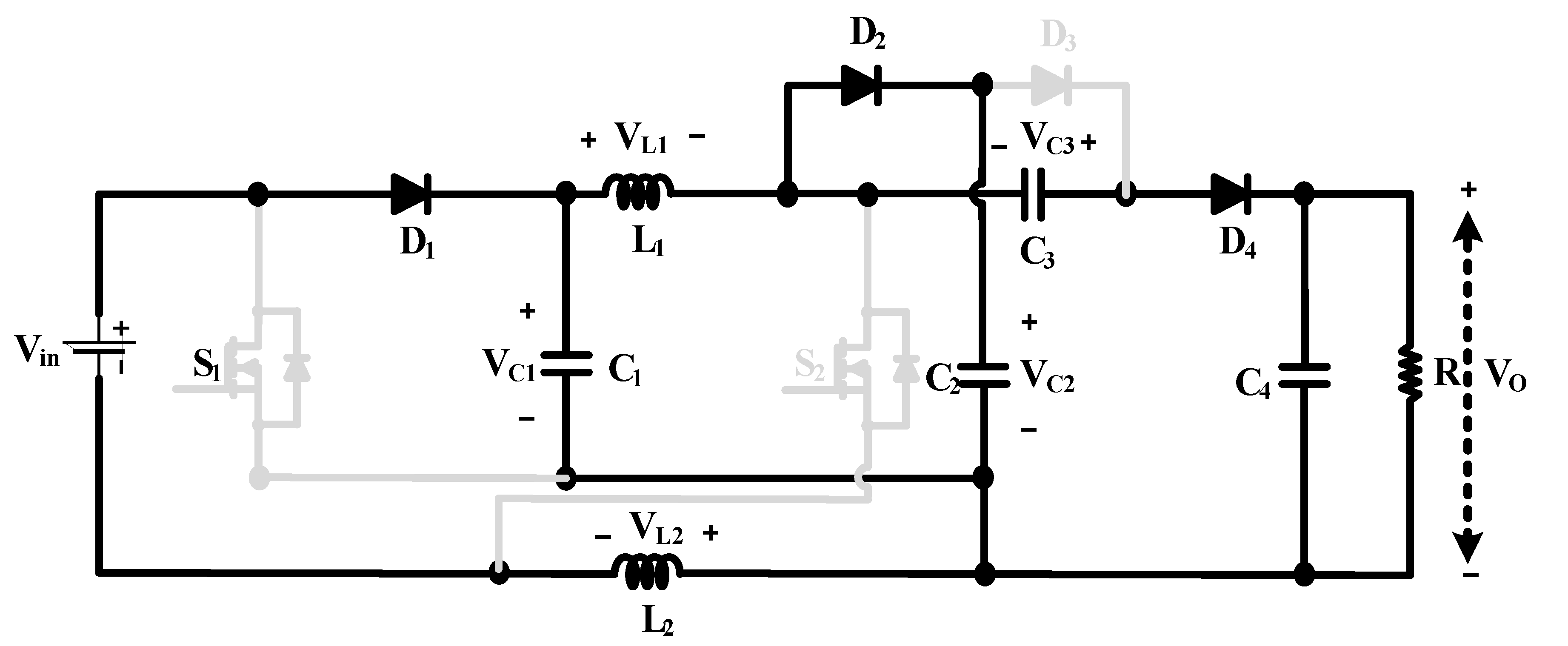
2. Proposed Topology
2.1. Structure
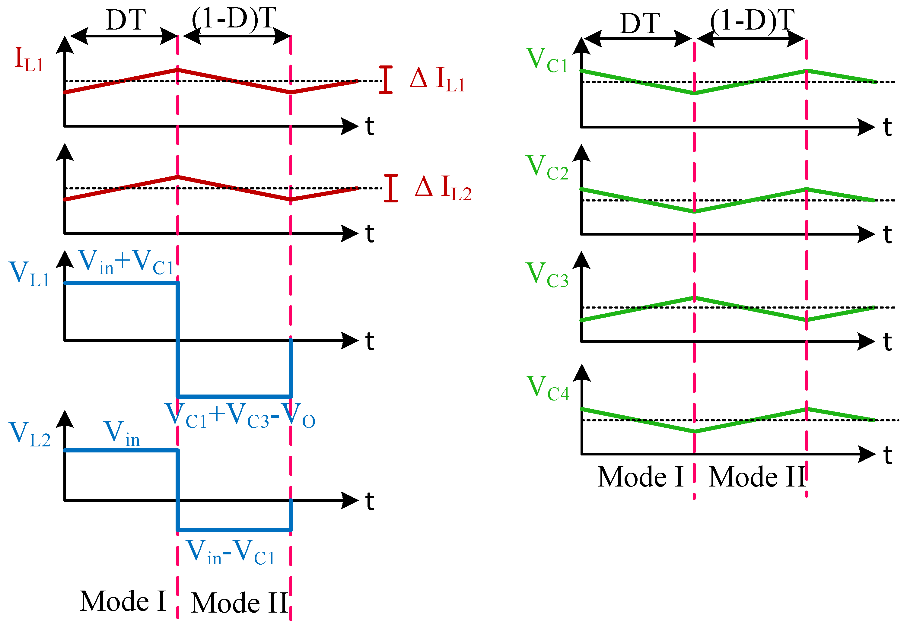
2.2. Working
2.3. Voltage and Current Stress across Components
3. Loss and Non-Ideal Gain Analysis
3.1. Bifurcation of Losses
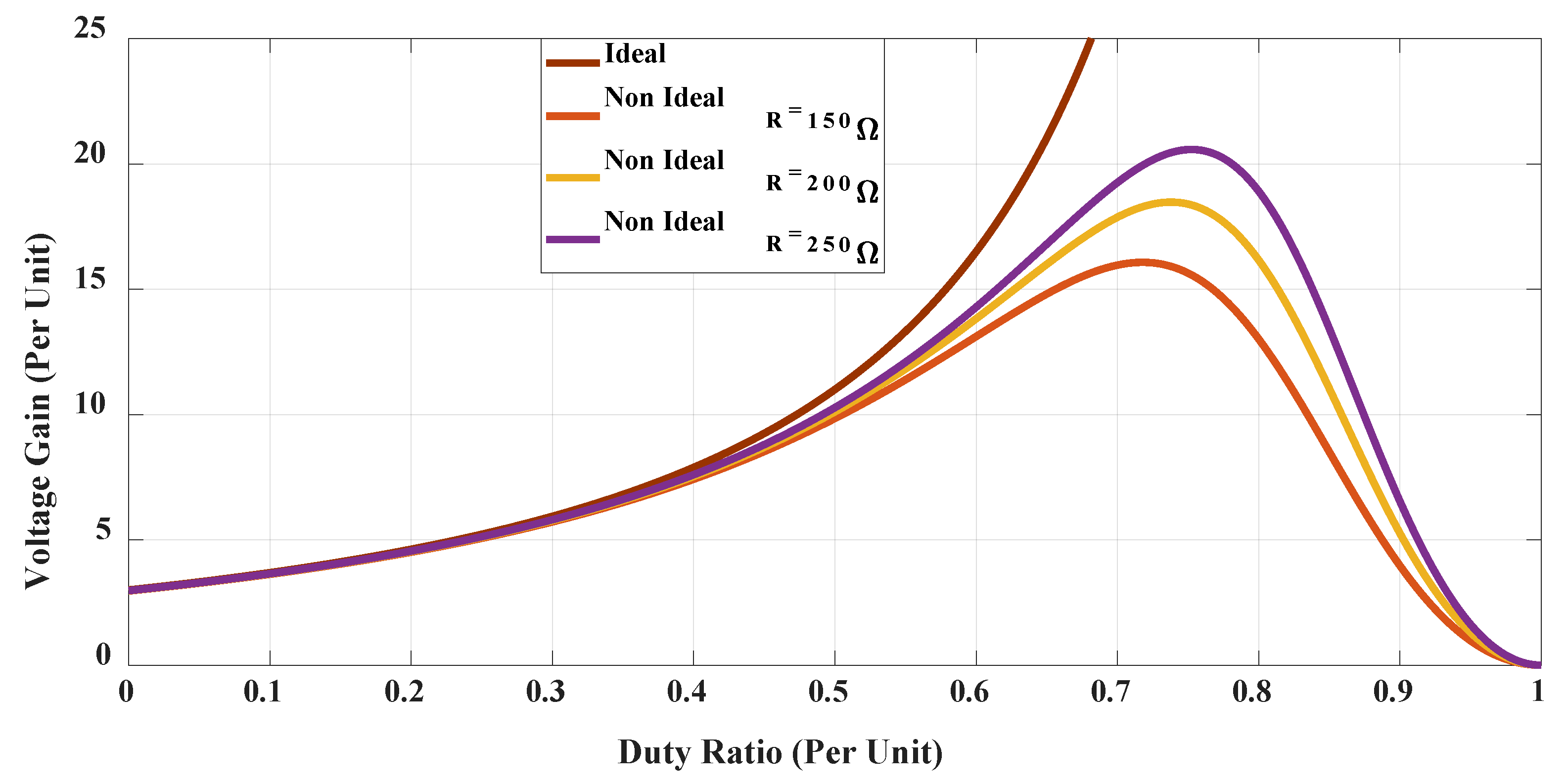
3.2. Non-Ideal Gain
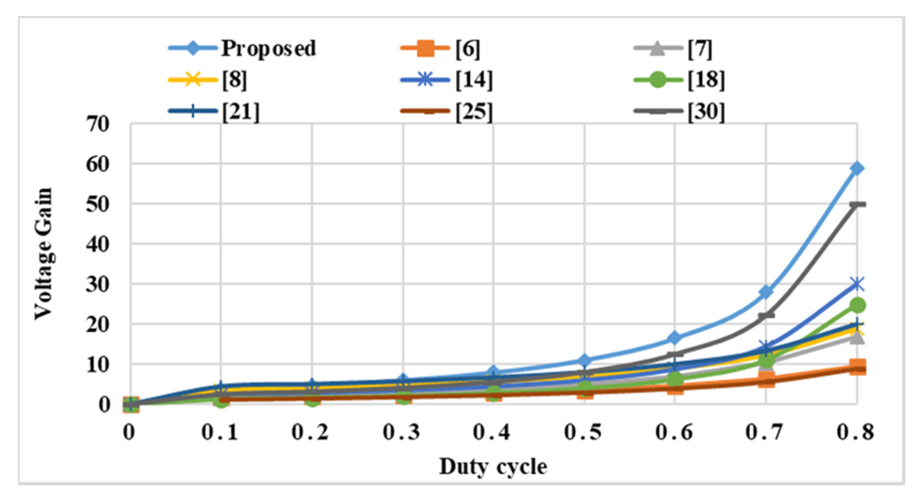
4. Comparison with Other Recent Topologies
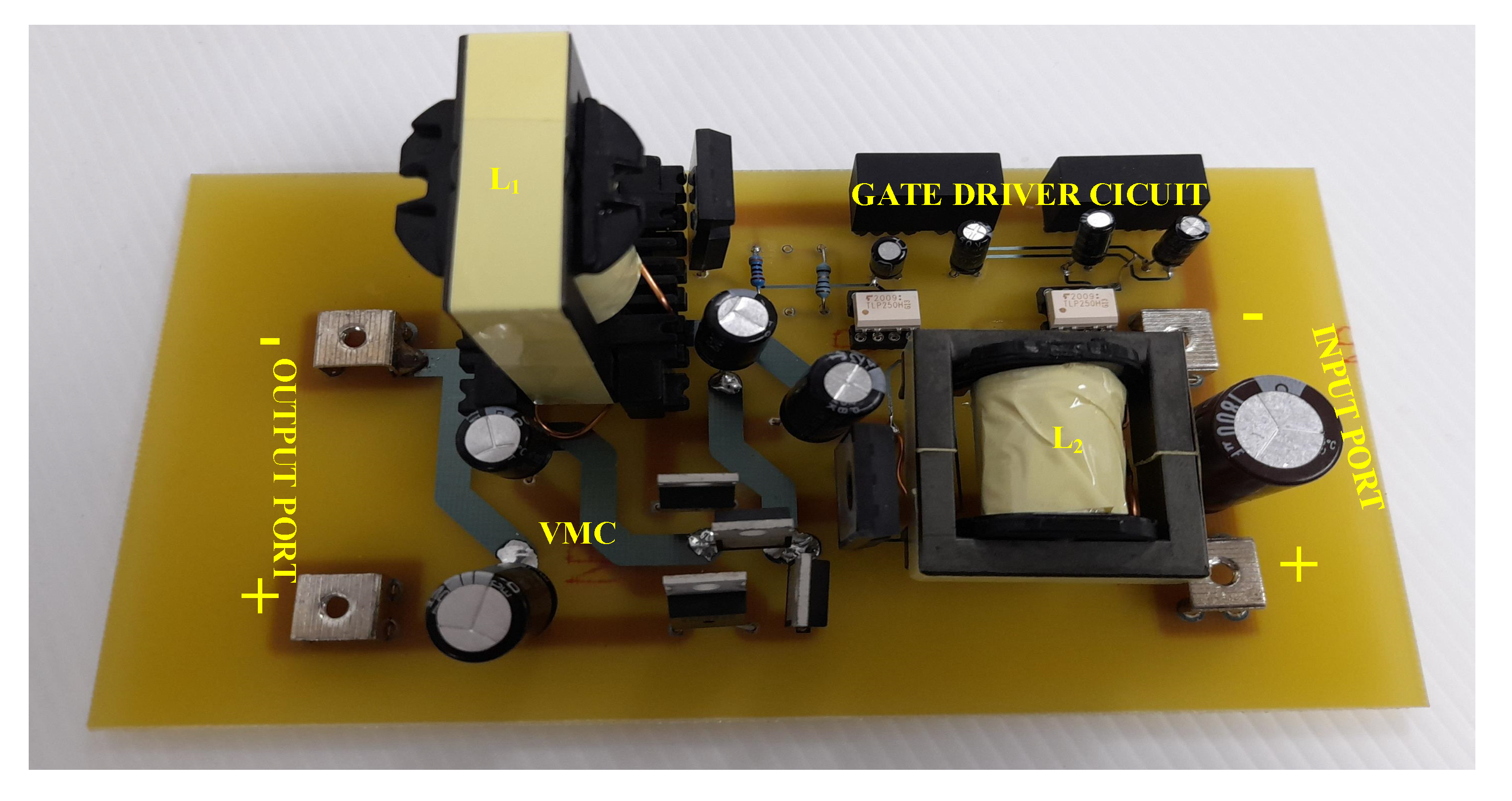
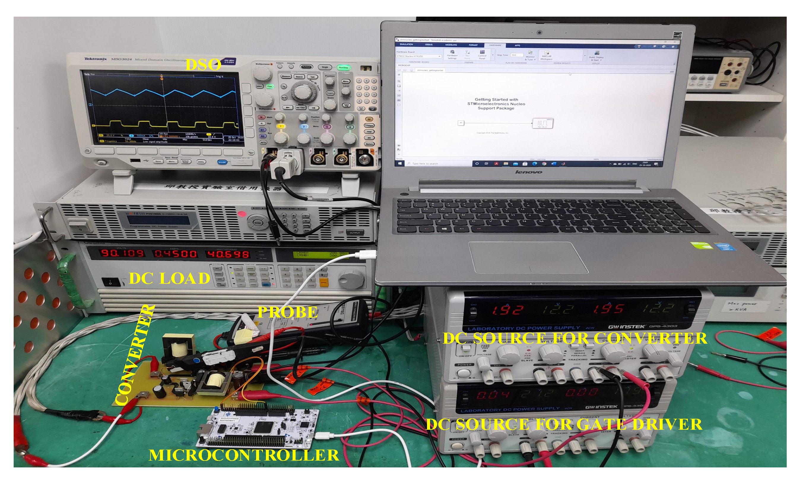
5. Experimental Verification of the Proposed Converter
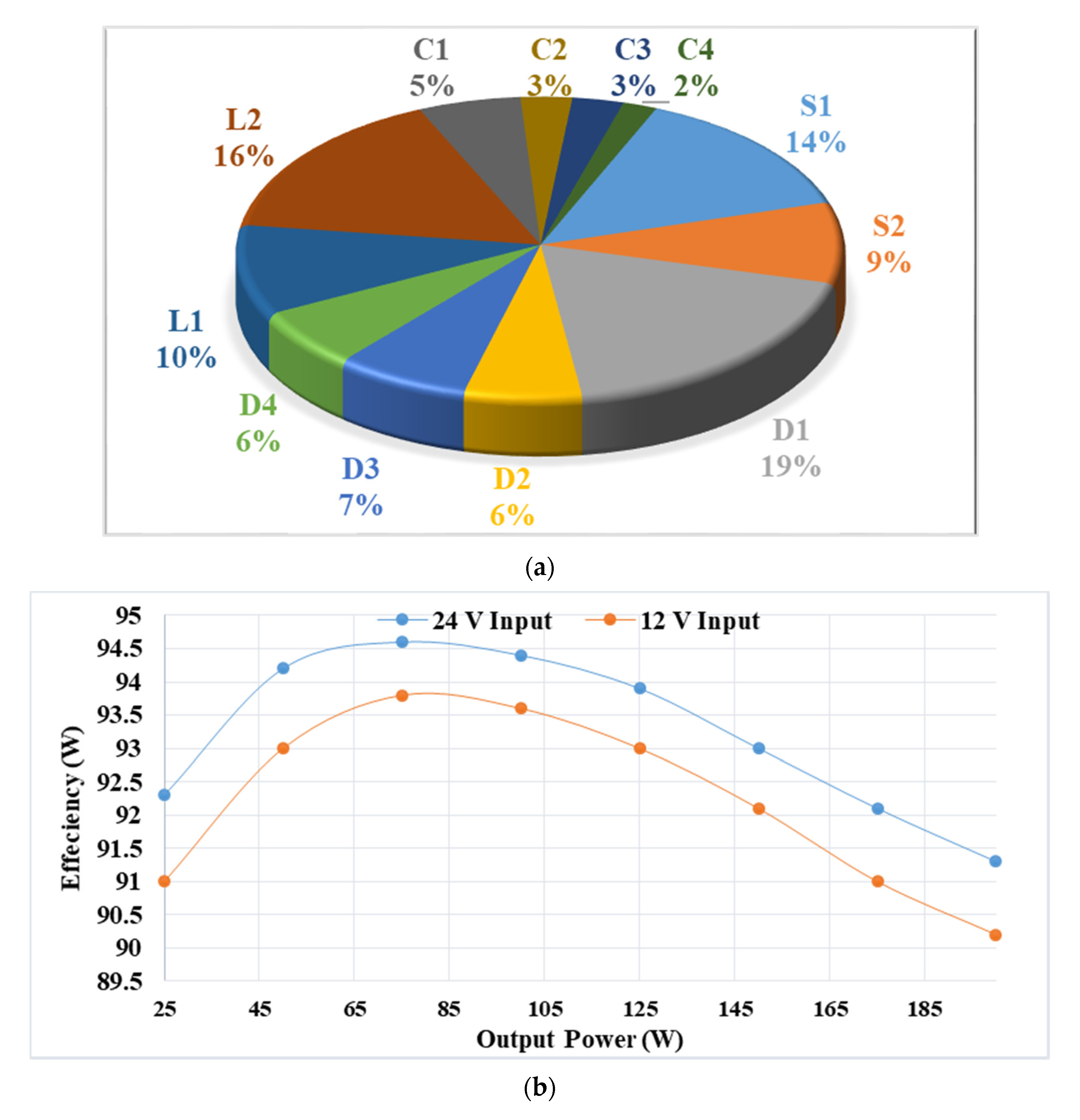
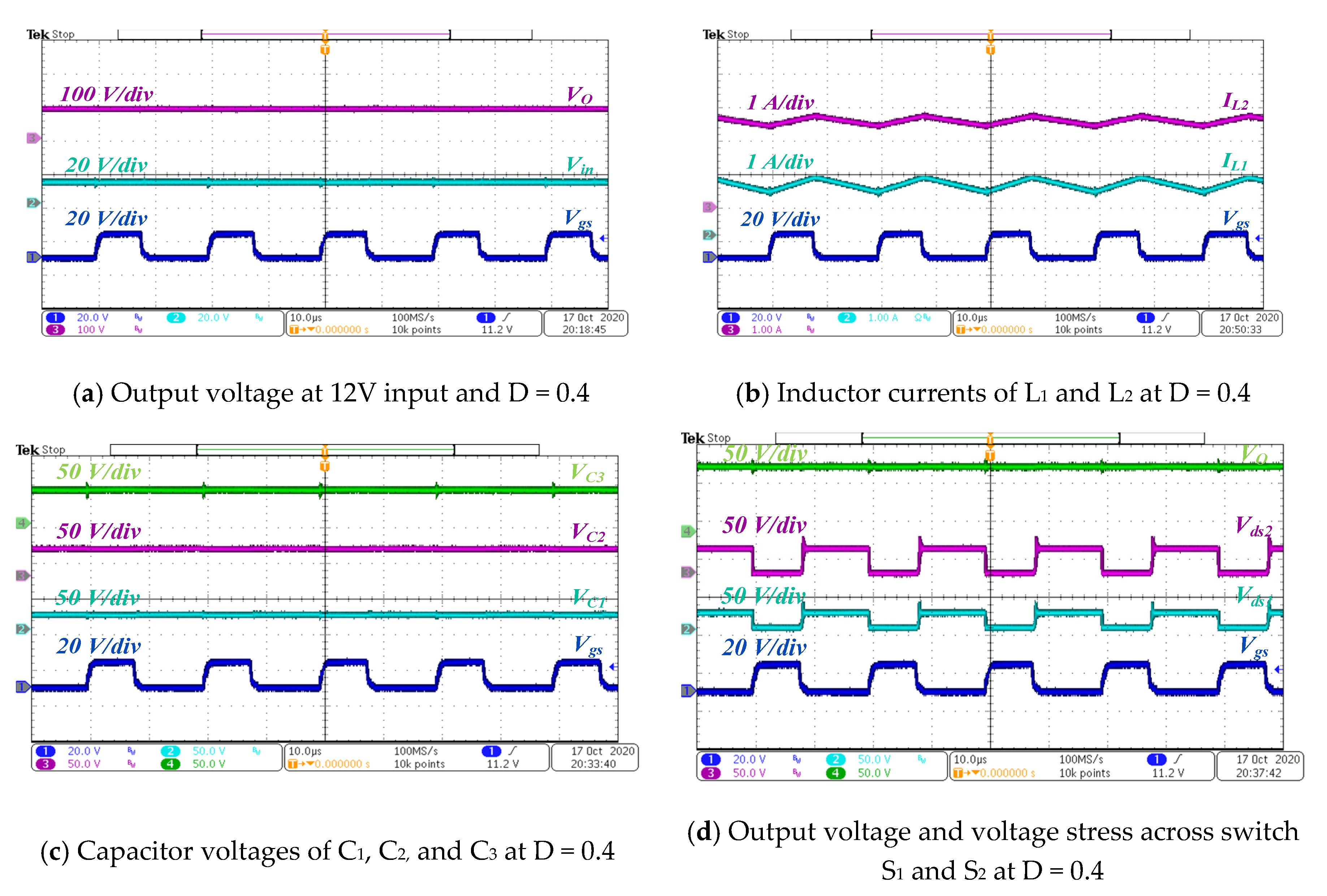
5.1. Experimental Results at Vin = 12 V
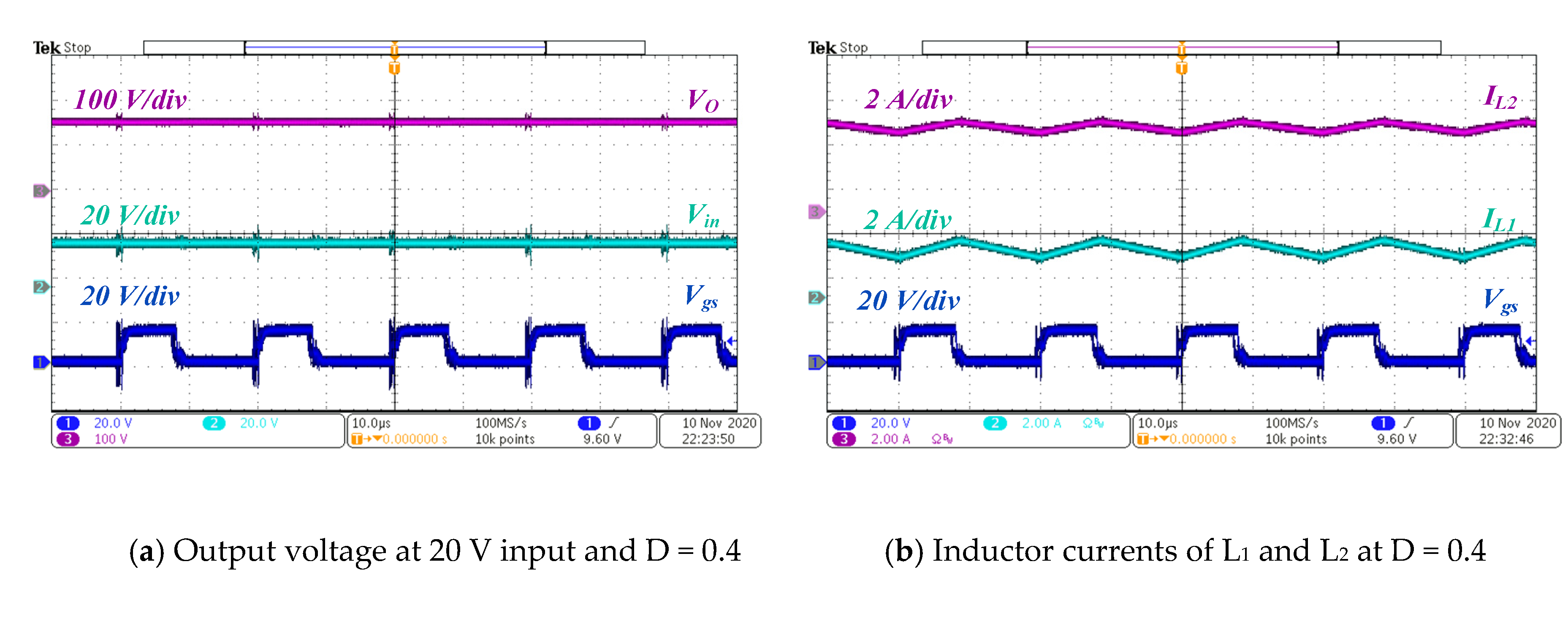
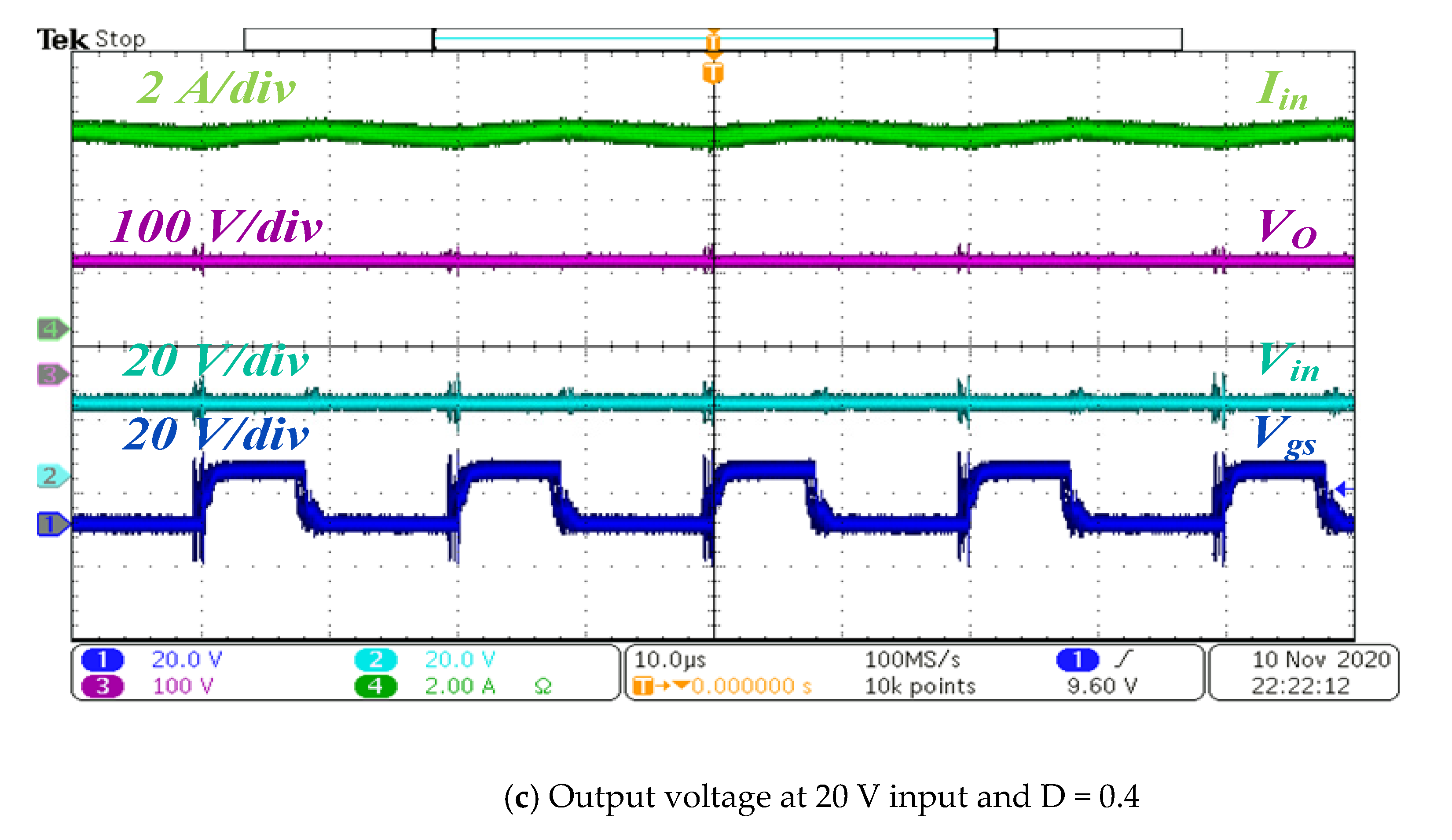
5.2. Experimental Results at Vin = 20 V
6. Conclusions
Author Contributions
Funding
Acknowledgments
Conflicts of Interest
References
- Forouzesh, M.; Siwakoti, Y.P.; Gorji, S.A.; Blaabjerg, F.; Lehman, B. Step-Up DC–DC Converters: A Comprehensive Review of Voltage-Boosting Techniques, Topologies, and Applications. IEEE Trans. Power Electron. 2017, 32, 9143–9178. [Google Scholar] [CrossRef]
- Tofoli, F.L.; De Paula, W.J.; Júnior, D.D.S.O.; Pereira, D.D.C. Survey on non-isolated high-voltage step-up dc–dc topologies based on the boost converter. IET Power Electron. 2015, 8, 2044–2057. [Google Scholar] [CrossRef] [Green Version]
- Rosas-Caro, J.C.; Ramirez, J.M.; Peng, F.Z.; Valderrabano, A. A DC-DC multilevel boost converter. IET Power Electron. 2010, 3, 129–137. [Google Scholar] [CrossRef]
- Sarikhani, A.; Allahverdinejad, B.; Hamzeh, M. A Non-Isolated Buck-Boost DC-DC Converter with Continuous Input Current for Photovoltaic Applications. IEEE J. Emerg. Sel. Top. Power Electron. 2020, 1. [Google Scholar] [CrossRef]
- Malik, M.Z.; Chen, H.; Nazir, M.S.; Khan, I.A.; Abdalla, A.N.; Ali, A.; Chen, W. A New Efficient Step-Up Boost Converter with CLD Cell for Electric Vehicle and New Energy Systems. Energies 2020, 13, 1791. [Google Scholar] [CrossRef] [Green Version]
- Saravanan, S.; Babu, N.R. Design and Development of Single Switch High Step-Up DC–DC Converter. IEEE J. Emerg. Sel. Top. Power Electron. 2017, 6, 855–863. [Google Scholar] [CrossRef]
- Tang, Y.; Fu, D.; Wang, T.; Xu, Z. Hybrid Switched-Inductor Converters for High Step-Up Conversion. IEEE Trans. Ind. Electron. 2015, 62, 1480–1490. [Google Scholar] [CrossRef]
- Tang, Y.; Wang, T.; He, Y. A Switched-Capacitor-Based Active-Network Converter With High Voltage Gain. IEEE Trans. Power Electron. 2014, 29, 2959–2968. [Google Scholar] [CrossRef]
- Faridpak, B.; Bayat, M.; Nasiri, M.; Samanbakhsh, R.; Farrokhifar, M. Improved Hybrid Switched Inductor/Switched Capacitor DC–DC Converters. IEEE Trans. Power Electron. 2020, 36, 3053–3062. [Google Scholar] [CrossRef]
- Wu, G.; Ruan, X.; Ye, Z. Nonisolated High Step-Up DC–DC Converters Adopting Switched-Capacitor Cell. IEEE Trans. Ind. Electron. 2015, 62, 383–393. [Google Scholar] [CrossRef]
- Duong, T.-D.; Nguyen, M.-K.; Tran, T.-T.; Lim, Y.-C.; Choi, J.-H. Transformerless High Step-Up DC-DC Converters with Switched-Capacitor Network. Electron. 2019, 8, 1420. [Google Scholar] [CrossRef] [Green Version]
- De Andrade, J.M.; Salvador, M.A.; Coelho, R.F.; Lazzarin, T.B. General Method for Synthesizing High Gain Step-Up DC–DC Converters Based on Differential Connections. IEEE Trans. Power Electron. 2020, 35, 13239–13254. [Google Scholar] [CrossRef]
- Frivaldsky, M.; Hanko, B.; Prazenica, M.; Morgos, J. High Gain Boost Interleaved Converters with Coupled Inductors and with Demagnetizing Circuits. Energies 2018, 11, 130. [Google Scholar] [CrossRef] [Green Version]
- Lee, S.-W.; Do, H.-L. Quadratic Boost DC–DC Converter With High Voltage Gain and Reduced Voltage Stresses. IEEE Trans. Power Electron. 2019, 34, 2397–2404. [Google Scholar] [CrossRef]
- Hasanpour, S.; Siwakoti, Y.P.; Mostaan, A.; Blaabjerg, F. New Semiquadratic High Step-Up DC/DC Converter for Renewable Energy Applications. IEEE Trans. Power Electron. 2020, 36, 433–446. [Google Scholar] [CrossRef]
- Liu, Z.; Du, J.; Yu, B. Design Method of Double-Boost DC/DC Converter with High Voltage Gain for Electric Vehicles. World Electr. Veh. J. 2020, 11, 64. [Google Scholar] [CrossRef]
- Loranca-Coutiño, J.; Villarreal-Hernandez, C.A.; Mayo-Maldonado, J.C.; Valdez-Resendiz, J.E.; Lopez-Nuñez, A.R.; Ruiz-Martinez, O.F.; Rosas-Caro, J.C. High Gain Boost Converter with Reduced Voltage in Capacitors for Fuel-Cells Energy Generation Systems. Electronics 2020, 9, 1480. [Google Scholar] [CrossRef]
- Shahir, F.M.; Babaei, E. A new structure for non-isolated boost dc-dc converter based on voltage-lift technique. In Proceedings of the 8th Power Electronics, Drive Systems & Technologies Conference (PEDSTC), Mashhad, Iran, 14–16 February 2017; pp. 25–30. [Google Scholar]
- Alzahrani, A.; Ferdowsi, M.; Shamsi, P. A Family of Scalable Non-Isolated Interleaved DC-DC Boost Converters With Voltage Multiplier Cells. IEEE Access 2019, 7, 11707–11721. [Google Scholar] [CrossRef]
- Meraj, M.; Bhaskar, M.S.; Iqbal, A.; Al-Emadi, N.; Rahman, S. Interleaved Multilevel Boost Converter With Minimal Voltage Multiplier Components for High-Voltage Step-Up Applications. IEEE Trans. Power Electron. 2020, 35, 12816–12833. [Google Scholar] [CrossRef]
- Pan, C.-T.; Chuang, C.-F.; Chu, C.-C. A Novel Transformer-less Adaptable Voltage Quadrupler DC Converter with Low Switch Voltage Stress. IEEE Trans. Power Electron. 2014, 29, 4787–4796. [Google Scholar] [CrossRef]
- Padmavathi, P.; Natarajan, S. Single switch quasi Z-source based high voltage gain DC-DC converter. Int. Trans. Electr. Energy Syst. 2020, 30, 1–25. [Google Scholar] [CrossRef]
- Meinagh, F.A.A.; Yuan, J.; Yang, Y. Analysis and design of a high voltage-gain quasi-Z-source DC–DC converter. IET Power Electron. 2020, 13, 1837–1847. [Google Scholar] [CrossRef]
- Martinez, W.; Cortes, C.; Yamamoto, M.; Imaoka, J. Effect of inductor parasitic resistances on the voltage gain of high step-up DC–DC converters for electric vehicle applications. IET Power Electron. 2018, 11, 1628–1639. [Google Scholar] [CrossRef]
- Karthikeyan, M.; Elavarasu, R.; Ramesh, P.; Bharatiraja, C.; Padmanaban, S.; Mihet-Popa, L.; Mitolo, M. A Hybridization of Cuk and Boost Converter Using Single Switch with Higher Voltage Gain Compatibility. Energies 2020, 13, 2312. [Google Scholar] [CrossRef]
- Lakshmi, M.; Hemamalini, S. Nonisolated High Gain DC–DC Converter for DC Microgrids. IEEE Trans. Ind. Electron. 2018, 65, 1205–1212. [Google Scholar] [CrossRef]
- Yang, P.; Xu, J.; Zhou, G.; Zhang, S. A new quadratic boost converter with high voltage step-up ratio and reduced voltage stress. In Proceedings of the 7th International Power Electronics and Motion Control Conference, Harbin, China, 2–5 June 2012; pp. 1164–1168. [Google Scholar]
- Jalilzadeh, T.; Rostami, N.; Babaei, E.; Maalandish, M. Non-Isolated Topology for High Step-Up DC-DC Converters. IEEE J. Emerg. Sel. Top. Power Electron. 2018, 1. [Google Scholar] [CrossRef]
- Babaei, E.; Maheri, H.M.; Sabahi, M.; Hosseini, S.H. Extendable Nonisolated High Gain DC–DC Converter Based on Active–Passive Inductor Cells. IEEE Trans. Ind. Electron. 2018, 65, 9478–9487. [Google Scholar] [CrossRef]
- Ahmad, J.; Zaid, M.; Sarwar, A.; Tariq, M.; Sarwer, Z. A New Transformerless Quadratic Boost Converter with High Voltage Gain. Smart Sci. 2020, 1–21. [Google Scholar] [CrossRef]
- Ahmad, J.; Pervez, I.; Sarwar, A.; Tariq, M.; Fahad, M.; Chakrabortty, R.K.; Ryan, M.J. Performance Analysis and Hardware-In-the-Loop (HIL) Validation of Single Switch High Voltage Gain DC-DC Converters for MPP Tracking in Solar PV System. IEEE Access 2020, 1. [Google Scholar] [CrossRef]


| Component | Voltage Stress (Volt) | Average Current During Their Conduction (Amp) | Average Current for the Complete Cycle (Amp) | RMS Current (Amp) |
|---|---|---|---|---|
| S1 | ||||
| S2 | ||||
| D1 | ||||
| D2 | ||||
| D3 | ||||
| D4 |
| Topology | NL (Inductors) | NC (Capacitors) | NSW (Switches) | ND (Diodes) | M | S |
|---|---|---|---|---|---|---|
| [6] | 2 | 4 | 1 | 4 | ||
| [7] | 4 | 1 | 2 | 7 | ||
| [8] | 2 | 3 | 2 | 3 | ||
| [14] | 1+1 coupled inductor | 3 | 1 | 5 | ||
| [18] | 2 | 2 | 1 | 3 | ||
| [21] | 2 | 4 | 2 | 4 | ||
| [25] | 2 | 3 | 1 | 2 | ||
| [30] | 3 | 3 | 1 | 5 | ||
| [31] | 3 | 3 | 1 | 5 | ||
| Proposed | 2 | 4 | 2 | 4 |
| Elements | Specification |
|---|---|
| Input Voltage (Vin) | 12 V/20 V |
| Maximum Output Power | 200 W |
| Switching Frequency | 50 kHz |
| Load Resistance | R = 200/250 Ω, Electronic load simulator |
| Inductors | L1 = 550 µH and L2 = 330 µH |
| Capacitors | C1 = 220µF/63V, C2 = C3 = 47 µF/100 V and C4 = 47 µF/200 V |
| Power MOSFET (S1 and S2) | SPW52N50C3 |
| Diodes (D1, D2, D3 and D4) | PFCD86 |
| Gate Drivers IC | TLP250H |
| Gate Driver Voltage Regulator IC | MCWI03-48S15 |
| Microcontroller | STM32 Nucleo H743ZI2 |
Publisher’s Note: MDPI stays neutral with regard to jurisdictional claims in published maps and institutional affiliations. |
© 2020 by the authors. Licensee MDPI, Basel, Switzerland. This article is an open access article distributed under the terms and conditions of the Creative Commons Attribution (CC BY) license (http://creativecommons.org/licenses/by/4.0/).
Share and Cite
Ahmad, J.; Zaid, M.; Sarwar, A.; Lin, C.-H.; Ahmad, S.; Sharaf, M.; Zaindin, M.; Firdausi, M. A Voltage Multiplier Circuit Based Quadratic Boost Converter for Energy Storage Application. Appl. Sci. 2020, 10, 8254. https://doi.org/10.3390/app10228254
Ahmad J, Zaid M, Sarwar A, Lin C-H, Ahmad S, Sharaf M, Zaindin M, Firdausi M. A Voltage Multiplier Circuit Based Quadratic Boost Converter for Energy Storage Application. Applied Sciences. 2020; 10(22):8254. https://doi.org/10.3390/app10228254
Chicago/Turabian StyleAhmad, Javed, Mohammad Zaid, Adil Sarwar, Chang-Hua Lin, Shafiq Ahmad, Mohamed Sharaf, Mazen Zaindin, and Muhammad Firdausi. 2020. "A Voltage Multiplier Circuit Based Quadratic Boost Converter for Energy Storage Application" Applied Sciences 10, no. 22: 8254. https://doi.org/10.3390/app10228254