Prediction of a Two-Transistor Vertical QNOT Gate


Department of Electronic Engineering, Gachon University, Seongnam 13120, Korea
*
Author to whom correspondence should be addressed.
Appl. Sci. 2020, 10(21), 7597; https://doi.org/10.3390/app10217597
Submission received: 23 September 2020
/
Revised: 21 October 2020
/
Accepted: 27 October 2020
/
Published: 29 October 2020
(This article belongs to the Special Issue Applications of Nano-Electronic Devices)
Abstract
:A new design of quaternary inverter (QNOT gate) is proposed by means of finite-element simulation. Traditionally, increasing the number of data levels in digital logic circuits was achieved by increasing the number of transistors. Our QNOT gate consists of only two transistors, resembling the binary complementary metal-oxide-semiconductor (CMOS) inverter, yet the two additional levels are generated by controlling the charge-injection barrier and electrode overlap. Furthermore, these two transistors are stacked vertically, meaning that the entire footprint only consumes the area of one single transistor. We explore several key geometrical and material parameters in a series of simulations to show how to systematically modulate and optimize the quaternary logic behaviors.
1. Introduction
The current electronics era was made possible by digital systems that maximize their simplicity in converting, processing, and memorizing a wide range of data into only two available electrical signal levels (“0” and “1”). However, such a standard binary logic architecture seems to hardly meet the increasing requirements for larger information capacities, which laid out the foundation of multi-valued logic (MVL) systems with n ≥ 3, where n is the number of distinguishable data levels [1,2,3]. To date, the realization of MVL has no fully established protocols; thus, various strategies are being pursued at the materials, device, and system levels [4,5,6]. For instance, Kobashi et al., in 2018, proposed a ternary (n = 3) inverter based on a lateral heterojunction of organic semiconductors [7,8]. In 2019, Yoo et al. proposed a full-swing ternary circuit using a negative transconductance heterojunction transistor with a modified structure [9]. Such reports suggested that, up to n = 3, a two-transistor topology can be effectively maintained (one unipolar and one anti-ambipolar). However, for a higher n, previous research mostly adopted circuit-based implementations with the number of transistors roughly corresponding to the number of data levels [10,11], implying the huge technological interest in advanced designs that reduce the transistor count.
In this study, we demonstrate an aggressive projection of quaternary (n = 4) digital inverter (or QNOT gate) made of only two field-effect transistors (FETs), by carrying out physically based finite-element simulation. In addition to saving the number of transistors, our proposed logic gate circuit is built by vertical (or three dimensional, 3-D) stacking of its component transistors, also showing the high potential for area-efficient on-chip deployment. In short, this particular geometry combines the two important trending design concepts in current electronics research, namely MVL and 3-D integration, in enabling a greatly simplified QNOT gate with a more efficient use of raw materials, manufacturing resources, and physical support areas. Importantly, the systematical variation of simulation parameters provides an in-depth understanding of how such an operation is obtained and also offers practical engineering guidelines toward targeted performances, which are intended to motivate wide-ranging experimental follow-ups.
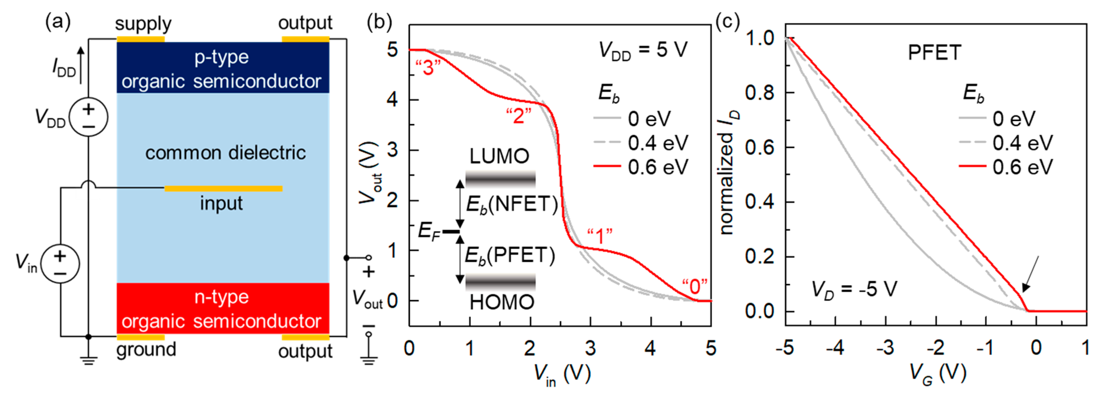
2. Methods
A finite-element drift-diffusion simulation package (Silvaco ATLAS) was used for this study. Organic semiconductors provide viable routes toward low-cost flexible electronics, by virtue of their secondary bonding nature. However, printed layers can have a feature size that is much larger than those patterned by conventional lithography. In this context, the vertical integration is of particular interest to printed organic electronics [12,13]. We, therefore, employed geometries and parameters relevant to organic materials and devices, yet some of the results will be extendable to other semiconductor platforms. The two-transistor, five-electrode circuit was defined according to the structure depicted in Figure 1a. The single gate electrode embedded in the common dielectric serves as the input node, where the input voltage (Vin) is applied. In the base structure, this input electrode is at the middle of the dielectric and is aligned to have no vertical overlap with the source and drain electrodes. The organic semiconductor thickness (tosc) is 50 nm (base structure), and the dielectric thickness (tdiel) is 100 nm. The channel length (L) and width (W) are 50 and 1000 µm, respectively. The dielectric constant of gate dielectric is 3.5. All electrodes are metallic with the work function of 4.5 eV. The p-type FET (PFET) and n-type FET (NFET) are made symmetric both structurally and energetically, with the carrier mobility of 1 cm2 V−1 s−1, the bandgap of 2 eV, and the effective density of states of 1020 cm−3. The high-occupied molecular orbital (HOMO) and lowest unoccupied molecular orbital (LUMO) energies of the respective semiconductors are systematically varied to generate different charge-injection barriers (Eb) [14]. The supply electrode is positioned on top of PFET, and the supply voltage (VDD) is applied to this node, in reference to the ground on the NFET side. The two drain electrodes are declared as the single floating numerical node, where the output voltage (Vout) is measured. The terminal characteristics (voltages and currents) along with the internal carrier distributions are self-consistently calculated for the whole circuit, by solving the coupled Poisson’s and drift-diffusion equations, under the Boltzmann carrier statistics and based on the Newton method.
3. Results and Discussion
The proposed layout in Figure 1a is basically analyzed in our previous work on the vertical 3-D organic inverter, which focuses on the voltage-gain improvement by increasing the contact resistance of FETs [13]. Here, we demonstrate for the first time that a substantial increase in Eb at both FETs can dramatically transform the simple 2-level inverter into a fully functional QNOT gate, without any structural modification. Figure 1b shows the simulation results of the voltage-transfer characteristics (VTCs) of the circuit in Figure 1a, at VDD = 5 V. The parametric variation of Eb was introduced with no change in electrode work function, but by energetically moving the semiconductor HOMO and LUMO levels together keeping the same bandgap (Figure 1b inset). The VTCs reveal that an initial departure from an ideal ohmic contact (Eb = 0 eV) to a blocking one (Eb = 0.4 eV) actually provides a sharper data transition from high to low Vout [13]. Surprisingly, it was found that an Eb of 0.6 eV substantially changes the shape of VTC, where the four data levels (“0”, “1”, “2”, and “3”) are clearly identifiable. To gain a first insight into its mechanism, we additionally performed simulations of individual FETs. As shown in Figure 1c, the normalized saturation-regime transfer curve of the PFET at a drain voltage (VD) of −5 V shows a quadratic shape with regard to gate voltage (VG) when Eb = 0 eV, suggesting no contact resistance effects [15,16]. In contrast, increasing Eb resulted in substantial deviation, exhibiting a quasi-linear behavior at Eb = 0.4 eV. At the Eb enabling the quaternary circuit, the drain current (ID) showed an apparent kink (arrow in Figure 1c), which is generally considered as the consequence of a substantial contact resistance [17,18,19]. Albeit with different biasing, this abrupt slope change on the transfer curve in part rationalizes the QNOT behavior of Figure 1b; this in fact translates into the existence of two distinct regimes with different resistance distribution ratios on a single transistor, during its on-off scan by Vin.
As the second requirement for QNOT functionality (in addition to Eb), the absence of geometrical overlap between the gate (input) and source/drain electrodes is addressed. Figure 2a is the side-by-side comparison of the cases of no overlap (base structure) and the full overlap with an extended gate electrode. Clearly, there is no quaternary effect in the modified circuit with a full electrode overlap. To further our understanding of underlying mechanism, we extracted the charge-carrier distribution at each component device in a full simulated inverter (not from the individual transistor simulation such as that in Figure 1c). Especially, the focus was placed on visualizing the internal distribution at two newly developed data states, one at Vin = 2V (level “2”) and the other at Vin = 3 V (level “1”) (in conjunction with Figure 1b). Comparing Figure 2b,c reveals one important difference, which is the apparent carrier pinch-off at the supply node (i.e., source electrode) indicated by the arrow in the no-overlap data of Figure 2b. This actually reminds us of the special property of the source-gated transistor (SGTs), whose operation largely relies on this source pinch-off rather than the drain pinch-off prevailing in traditional FETs [20]. While it was known that such a behavior is fundamentally associated with a high-barrier contact (which is the case here), our data additionally prove that the pinch-off is more accentuated when there is no sufficient gate-source overlap to attract the injected charge carriers toward the channel surface. More importantly, it justifies the presence and absence of the two intermediate voltage levels, since such strong pinching-off at the no-overlap circuit dictates the stable establishment of the constant resistance regime between the complete turning-on and off. Figure 2d,e simply deliver the same message, based on the electron pinch-off at the no-overlap NFET (here the ground is the source) that forms the intermediate state between its full on-off switching.
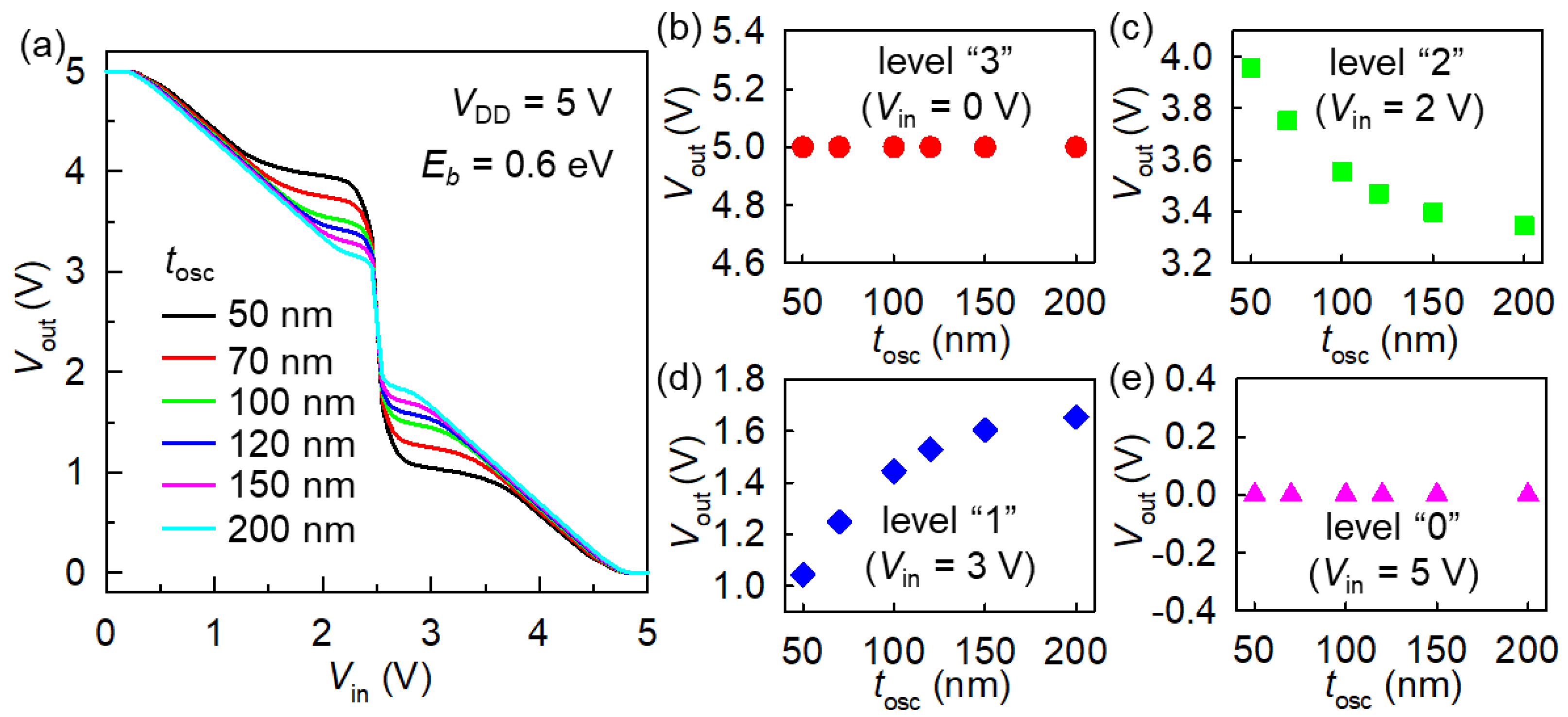
Now, we return to the base structure (Eb = 0.6 eV, no electrode overlap) and demonstrate the possibilities of VTC engineering. Firstly, the parameter tosc was found to have a significant impact on the level formation, as illustrated in the simulation results of Figure 3a upon changing tosc from 50 to 200 nm. The four output data levels, “3”, “2”, “1”, and “0”, were extracted at Vin = 0, 2, 3, and 5 V, respectively, from each VTC. As shown in Figure 3b–e, the semiconductor thickness significantly influences the two intermediate data voltages, with a clearly monotonous trend, meaning that a desired value can eventually be obtained through fine tuning of the layer thickness. Meanwhile, little or no impact of tosc was seen on the two extreme levels. This interesting phenomenon can be explained as follows. Since the QNOT behavior in our system originates from the Eb and the contact resistance thereof [13], an enlarged out-of-plane bulk film resistance at a thicker film can significantly modulate the VTC characteristics [14]. More specifically, the FET contact resistance becomes larger with a higher tosc in this staggered electrode architecture [21,22], affecting the establishment of the pinch-off region (see Figure 2b,d), thus pushing the “2” and “1” levels toward VDD/2 at the same time.
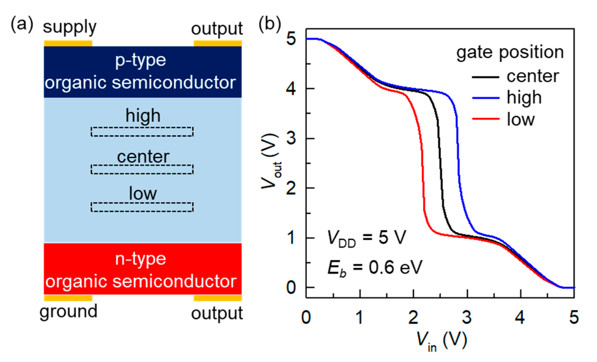
Secondly, the vertical positioning of the gate electrode was another efficient controlling factor. In fact, separately changing the PFET and NFET gate dielectric thicknesses is a traditional approach in a complementary metal-oxide-semiconductor (CMOS) binary inverter to relatively tune the strength of the transistors [23]. In our simulation, the total thickness of the common dielectric (tdiel) was fixed as 100 nm, yet the three in-dielectric positions of the gate electrode (center, high, and low) were compared as graphically illustrated in Figure 4a. The high or low position was made by moving the electrode from the center position by 25-nm upwardly or downwardly, respectively. Figure 4b shows that a systematic horizontal movement of the level “2” to “1” transition point was observed by changing the vertical gate position. This is understood as the outcome of the increase in the PFET strength (for the high position) or the NFET strength (for the low position) that redistributes the supplied VDD at different ratios, thus modulating the mid-transition Vin point. These results also re-confirm the contact-dominated QNOT mechanism, as evidenced by no practical change in the four data levels and the extreme transitions points, because these properties are mostly determined by the depleted source regions rather than the capacitively modulated channel regions [19].
Regarding the quaternary inverting behavior in this study, we can make several additional notes. As the Eb increases, the driving current (IDD) systematically decreases because of contact resistance. This in turn provides an additional advantage of low power consumption (total power is VDD multiplied by IDD) in the QNOT regime (Supplementary Figure S1). Another critical point is that a vertical coupling is essential to QNOT behavior. In our proposed structure, a strong electric field appears between the supply and ground nodes (see Figure 1a), which helps establish an elongated accumulation channel at the source region even without a gate overlap, laying a foundation for the source pinch-off and associated quaternary operation. In stark contrast, comparative simulations showed that both the source and drain contact regions are fully depleted so that less currents flow in the horizontal inverter with no indication of pinch-off and QNOT functionality (Supplementary Figure S2). Also note that a relatively large tdiel is used for the relevance to organic electronics. Additional simulations revealed that the operation voltage can be scaled down even in this structure, yet the intermediate levels become indistinct at a VDD below 3 V (Supplementary Figure S3).
4. Conclusions
This paper shed light on the technological feasibility of a simple two-transistor vertical QNOT gate. The physical simulation results showed that a substantial Eb and the absence of gate overlap are both required for the appearance of the four data voltage levels. In terms of the VTC engineering, the value of tosc and vertical gate re-positioning were found to be effective in altering the output levels and the mid-transition input voltage, respectively. A systematic correlation between the terminal characteristics, the FET behaviors, and the internal charge distributions established an operation mechanism relying on the source-contact pinch-off and the resulting resistive re-distribution. Our results strategically leveraged the power of material-device-system correlation in developing new structural functionalities, and are expected to serve as a motivation and guideline for next-generation quaternary and higher MVL digital electronics
Supplementary Materials
The following are available online at https://www.mdpi.com/2076-3417/10/21/7597/s1, Figure S1: Power consumption; Figure S2: Vertical and horizontal inverter comparison; Figure S3: Scaling property.
Author Contributions
Conceptualization, H.H. and C.-H.K.; methodology, H.H.; validation, C.-H.K.; formal analysis, H.H. and C.-H.K.; writing—original draft preparation, H.H.; writing—review and editing, C.-H.K.; supervision, C.-H.K. All authors have read and agreed to the published version of the manuscript.
Funding
This work was supported by the National Research Foundation of Korea (NRF) grant funded by the Korean government (MSIT) (NRF-2019R1C1C1003356), and by the Gachon University research fund of 2020 (GCU-202003000001).
Conflicts of Interest
The authors declare no conflict of interest.
References
- Gaudet, V. A survey and tutorial on contemporary aspects of multiple-valued logic and its application to microelectronic circuits. IEEE J. Emerg. Sel. Top. Circuits Syst. 2016, 6, 5–12. [Google Scholar] [CrossRef]
- Lv, W.; Fu, X.; Luo, X.; Lv, W.; Cai, J.; Zhang, B.; Wei, Z.; Liu, Z.; Zeng, Z. Multistate logic inverter based on black phosphorus/SnSeS heterostructure. Adv. Electron. Mater. 2019, 5, 1800416. [Google Scholar] [CrossRef] [Green Version]
- Jeong, J.W.; Choi, Y.-E.; Kim, W.-S.; Park, J.-H.; Kim, S.; Shin, S.; Lee, K.; Chang, J.; Kim, S.-J.; Kim, K.R. Tunnelling-based ternary metal–oxide–semiconductor technology. Nat. Electron. 2019, 2, 307–312. [Google Scholar] [CrossRef]
- Jin, N.; Chung, S.-Y.; Heyns, R.M.; Berger, P.R.; Yu, R.; Thompson, P.E.; Rommel, S.L. Tri-state logic using vertically integrated Si-SiGe resonant interband tunneling diodes with double NDR. IEEE Electron Device Lett. 2004, 25, 646–648. [Google Scholar] [CrossRef]
- Lee, L.; Hwang, J.; Jung, J.W.; Kim, J.; Lee, H.-I.; Heo, S.; Yoon, M.; Choi, S.; Long, N.V.; Park, J.; et al. ZnO composite nanolayer with mobility edge quantization for multi-value logic transistors. Nat. Commun. 2019, 10, 1998. [Google Scholar] [CrossRef] [Green Version]
- Shim, J.; Oh, S.; Kang, D.-H.; Jo, S.-H.; Ali, M.H.; Choi, W.-Y.; Heo, K.; Jeon, J.; Lee, S.; Kim, M.; et al. Phosphorene/rhenium disulfide heterojunction-based negative differential resistance device for multi-valued logic. Nat. Commun. 2016, 7, 13413. [Google Scholar] [CrossRef] [Green Version]
- Kobashi, K.; Hayakawa, R.; Chikyow, T.; Wakayama, Y. Multi-valued logic circuits based on organic anti-ambipolar transistors. Nano Lett. 2018, 18, 4355–4359. [Google Scholar] [CrossRef] [PubMed]
- Kim, C.-H.; Hayakawa, R.; Wakayama, Y. Fundamentals of organic anti-ambipolar ternary inverters. Adv. Electron. Mater. 2020, 6, 1901200. [Google Scholar] [CrossRef]
- Yoo, H.; On, S.; Lee, S.B.; Cho, K.; Kim, J.-J. Negative transconductance heterojunction organic transistors and their application to full-swing ternary circuits. Adv. Mater. 2019, 31, 1808265. [Google Scholar] [CrossRef] [PubMed]
- Moaiyeri, M.H.; Navi, K.; Hashemipour, O. Design and evaluation of CNFET-based quaternary circuits. Circuits Syst. Signal Process. 2012, 31, 1631–1652. [Google Scholar] [CrossRef]
- Ebrahimi, S.A.; Reshadinezhad, M.R.; Bohlooli, A.; Shahsavari, M. Efficient CNTFET-based design of quaternary logic gates and arithmetic circuits. Microelectron. J. 2016, 53, 156–166. [Google Scholar] [CrossRef]
- Kwon, J.; Takeda, Y.; Shiwaku, R.; Tokito, S.; Cho, K.; Jung, S. Three-dimensional monolithic integration in flexible printed organic transistors. Nat. Commun. 2019, 10, 54. [Google Scholar] [CrossRef] [Green Version]
- Han, H.; Kim, C.-H. Unexpected benefits of contact resistance in 3D organic complementary inverters. Adv. Electron. Mater. 2020, 6, 1900879. [Google Scholar] [CrossRef]
- Kim, C.-H. Contact resistance in organic transistors: Use it or remove it. Appl. Phys. Rev. 2020, 7, 031306. [Google Scholar] [CrossRef]
- Yang, T.; Wu, Q.; Dai, F.; Huang, K.; Xu, H.; Liu, C.; Chen, C.; Hu, S.; Liang, X.; Liu, X.; et al. Understanding, optimizing, and utilizing nonideal transistors based on organic or organic hybrid semiconductors. Adv. Funct. Mater. 2019, 30, 1903889. [Google Scholar] [CrossRef]
- Wu, X.; Jia, R.; Pan, J.; Zhang, X.; Jie, J. Roles of interfaces in the ideality of organic field-effect transistors. Nanoscale Horiz. 2020, 5, 454–472. [Google Scholar] [CrossRef]
- Bittle, E.G.; Basham, J.I.; Jackson, T.N.; Jurchescu, O.D.; Gundlach, D.J. Mobility overestimation due to gated contacts in organic field-effect transistors. Nat. Commun. 2016, 7, 10908. [Google Scholar] [CrossRef] [Green Version]
- Kim, C.-H.; Thomas, S.; Kim, J.H.; Elliott, M.; Macdonald, J.E.; Yoon, M.-H. Potentiometric parameterization of dinaphtho[2,3-b:2′,3′-f]thieno[3,2-b]thiophene field-effect transistors with a varying degree of nonidealities. Adv. Electron. Mater. 2018, 4, 1700514. [Google Scholar] [CrossRef]
- Kim, C.-H.; Horowitz, G. Toward a fully analytical contact resistance expression in organic transistors. Materials 2019, 12, 1169. [Google Scholar] [CrossRef] [Green Version]
- Sporea, R.A.; Trainor, M.J.; Young, N.D.; Shannon, J.M.; Silva, S.R.P. Source-gated transistors for order-of-magnitude performance improvements in thin-film digital circuits. Sci. Rep. 2014, 4, 4295. [Google Scholar] [CrossRef] [PubMed] [Green Version]
- Kim, C.H.; Bonnassieux, Y.; Horowitz, G. Fundamental benefits of the staggered geometry for organic field-effect transistors. IEEE Electron Device Lett. 2011, 32, 1302–1304. [Google Scholar] [CrossRef] [Green Version]
- Altazin, S.; Clerc, R.; Gwoziecki, R.; Boudinet, D.; Ghibaudo, G.; Pananakakis, G.; Chartier, I.; Coppard, R. Analytical modeling of the contact resistance in top gate/bottom contacts organic thin film transistors. Org. Electron. 2011, 12, 897–902. [Google Scholar] [CrossRef]
- Kwon, J.; Kyung, S.; Yoon, S.; Kim, J.-J.; Jung, S. Solution-processed vertically stacked complementary organic circuits with inkjet-printed routing. Adv. Sci. 2016, 3, 1500439. [Google Scholar] [CrossRef] [PubMed] [Green Version]
Figure 1.
(a) Cross-sectional illustration and driving configuration of the proposed inverter circuit. (b) Simulated voltage-transfer characteristics (VTCs) showing the evolution from binary to quaternary logic. Inset: the energy diagram defining Eb at each field-effect transistor (FET) (EF is the source/drain metal Fermi level). (c) Normalized transfer curve of the p-type FET (PFET) at varying Eb.

Figure 2.
(a) Simulation results showing the direct impact of the gate-electrode length on VTC. (b,c) Hole concentration inside the PFET at Vin = 2 V (level “2”) under no and full overlap conditions. (d,e) Electron concentration inside the NFET at Vin = 3 V (level “1”) under no and full overlap conditions.

Figure 3.
(a) Change of VTC according to the variation of tosc. (b–e) Extraction of the Vout values at four data levels from the results in (a).
Figure 3.
(a) Change of VTC according to the variation of tosc. (b–e) Extraction of the Vout values at four data levels from the results in (a).

Figure 4.
(a) Illustration showing the structural variation by vertically re-positioning the common gate electrode inside the common dielectric layer. (b) VTC comparison for the three gate positions.
Figure 4.
(a) Illustration showing the structural variation by vertically re-positioning the common gate electrode inside the common dielectric layer. (b) VTC comparison for the three gate positions.

Publisher’s Note: MDPI stays neutral with regard to jurisdictional claims in published maps and institutional affiliations. |
© 2020 by the authors. Licensee MDPI, Basel, Switzerland. This article is an open access article distributed under the terms and conditions of the Creative Commons Attribution (CC BY) license (http://creativecommons.org/licenses/by/4.0/).
Share and Cite
MDPI and ACS Style
Han, H.; Kim, C.-H. Prediction of a Two-Transistor Vertical QNOT Gate. Appl. Sci. 2020, 10, 7597. https://doi.org/10.3390/app10217597
AMA Style
Han H, Kim C-H. Prediction of a Two-Transistor Vertical QNOT Gate. Applied Sciences. 2020; 10(21):7597. https://doi.org/10.3390/app10217597
Chicago/Turabian StyleHan, Heesung, and Chang-Hyun Kim. 2020. "Prediction of a Two-Transistor Vertical QNOT Gate" Applied Sciences 10, no. 21: 7597. https://doi.org/10.3390/app10217597
Note that from the first issue of 2016, this journal uses article numbers instead of page numbers. See further details here.