1. Introduction
Today, because photovoltaic (PV) energy is noiseless, pollution-free, non-radioactive and inexhaustible, PV grid-connection power systems are receiving increasing attention [
1,
2,
3]. For the PV grid-connected systems, inverters are necessary to convert the DC voltage of the PV panel to an AC voltage, and then supply power in parallel with utility-line. Therefore, many experts have invested in the research of the circuit architecture and control strategy of inverters [
4,
5,
6,
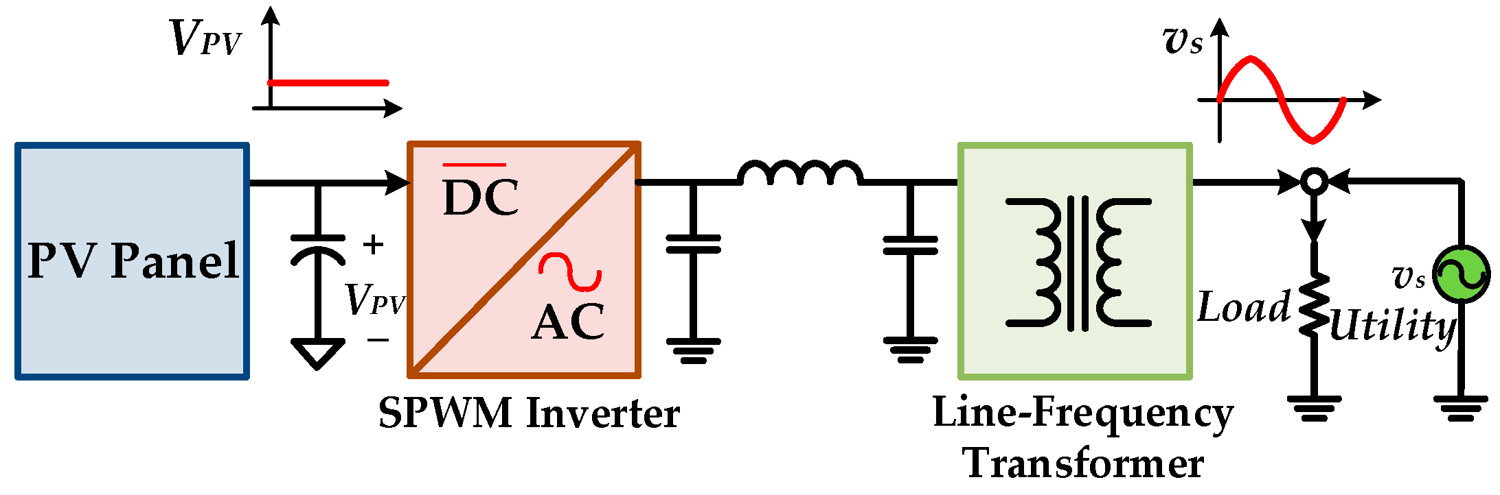
7]. The full-bridge voltage-source inverter is the popular topology in low-power PV grid-connected systems. However, due to its buck-typed conversion, a line-frequency transformer has to be inserted between the inverter and utility-line. This system structure greatly increases the volume, weight and cost of the system, and reduces the power density.
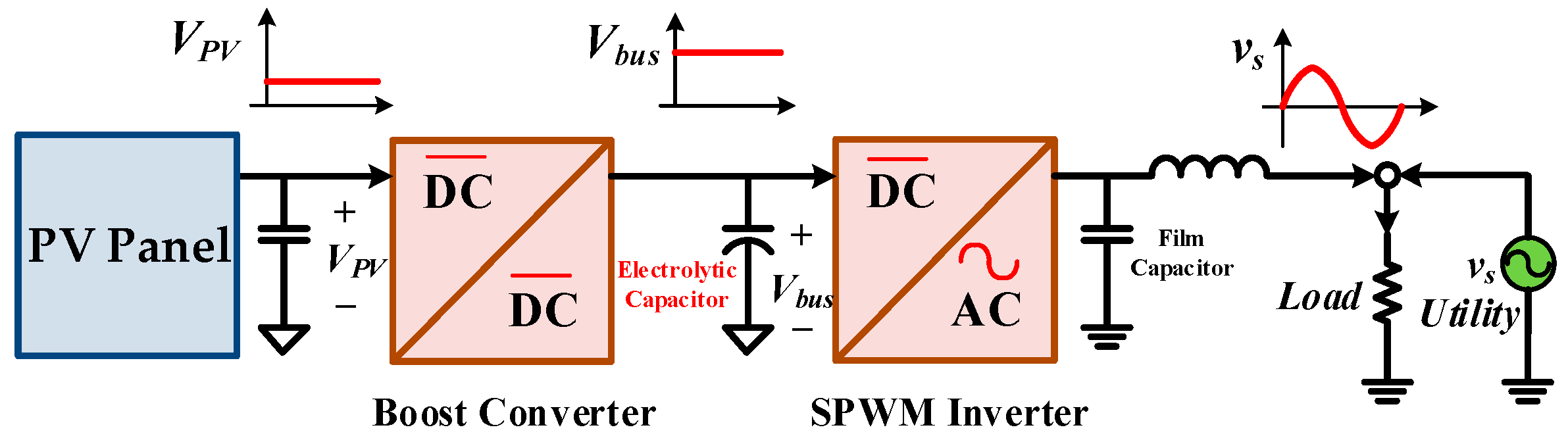
Inserting a boost converter to step-up the output voltage of the PV panel is the alternative solution. The boost converter can not only regulate PV output voltage but also achieve maximum power point tracking (MPPT) [
8,
9]. The main advantage of this two-stage cascade structure is the independent control of the power converters. It is easy to optimize the function of each stage, and the input voltage of the inverter is regulated. However, the disadvantages are the increase in the complexity of the system circuit, the increase in cost, and the reduction in reliability. The power loss due to multiple energy processing will reduce the overall system efficiency. The pseudo-dc-link inverters are proposed to improve these shortcomings [
10,
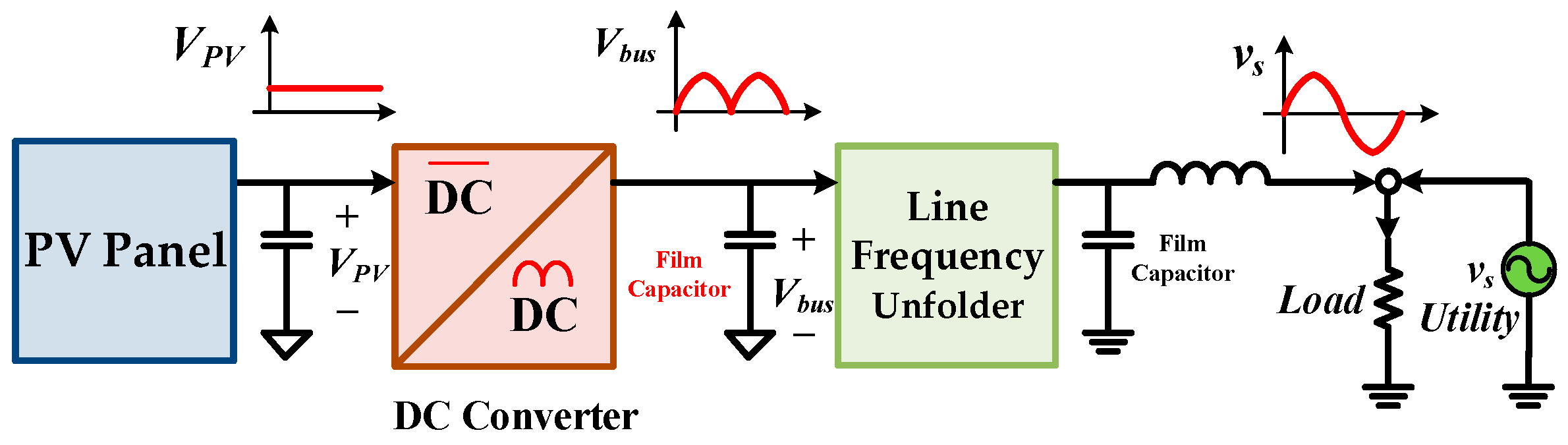
11]. In these inverters, a DC converter is used to generate a single-polarity rectified sine wave, and a line-frequency bridge unfolding circuit is used to switch the polarity of the output voltage. Since there is only single energy processing, power loss can be reduced to improve efficiency.
Among these high-efficiency inverters with pseudo-dc-link, the buck-boost type converters are widely used to implement non-isolated inverters for the photovoltaic grid-connected power system with wide-range input voltage fluctuation [
12,
13,
14,
15]. Furthermore, in order to obtain higher boosting capacity and meet the safety requirement of electrical isolation, isolated DC-DC converters, such as flyback converter, are often used to design isolated pseudo-dc-link inverters [
16,
17,
18,
19]. The flyback converter has the advantages of simple structure and easy control. However, because the transformer of the flyback converter needs to function as an inductor for energy storage, all energy needs to be temporarily stored in the transformer and then transferred to the output load, so its output power and efficiency are limited.
In order to improve the output power and conversion efficiency of the inverter with electrical isolation, the forward inverter is proposed [
20], where the forward converter is adopted to replace the flyback converter and to generate a rectified sine wave. However, since the forward converter needs a third winding of the transformer to reset its residual magnetic flux, the maximum duty ratio of the power switch is limited, thereby reducing the boosting capacity of the converter. The dual-switch forward inverter [
21] adds additional power switches, diodes, and a secondary winding to reset the residual magnetic flux of the transformer. The transformer can be operated in both of the first and third quadrants, but its volume and total circuit cost are greatly increased. Therefore, an active-clamp forward inverter is proposed in this paper. By replacing the traditional reset winding with an auxiliary switch and a clamp capacitor, the residual magnetic flux can be reset through the resonance of the clamp capacitor and the magnetizing inductor. In addition to recovering the energy of the magnetizing inductor back to the input, the power switch can also be turned on with zero voltage switching (ZVS) to reduce switching losses and effectively increase the efficiency of the inverter. Circuit configuration, operation principles, and design considerations will be presented sequentially in the following. Finally, a laboratory prototype of the proposed inverter is built accordingly to verify the feasibility of the proposed circuit architecture and the correctness of the theoretical analysis.
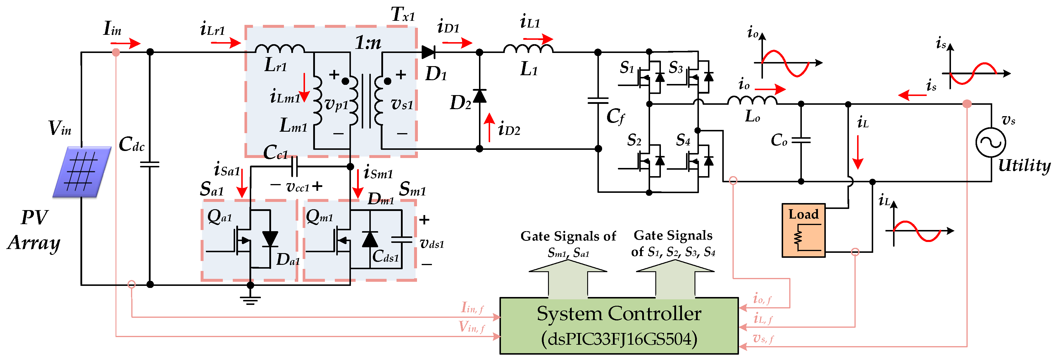
2. Circuit Configuration
As mentioned previously, the popular PV grid-connection systems need a line-frequency transformer or a boost converter to step-up output voltage. Their system block diagrams are shown in
Figure 1 and
Figure 2, respectively. In order to improve efficiency and reduce cost, the pseudo-dc-link inverters are proposed, as shown in
Figure 3. However, these inverters are non-isolated, which may not avoid the leakage current of the PV panel. Therefore, an active-clamp forward inverter featuring soft switching and electrical isolation is proposed in this paper.
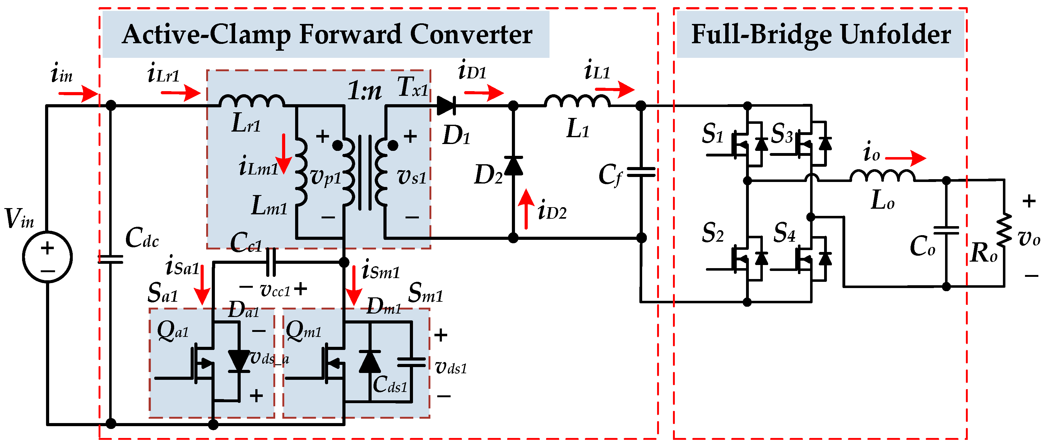
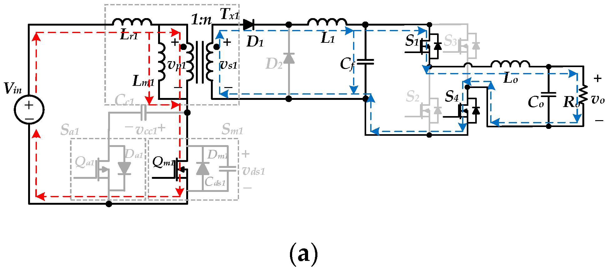
The circuit diagram of the proposed inverter is shown in
Figure 4. The active-clamp forward converter with zero voltage switching is used to generate the single-polarity rectified sine wave, and the full-bridge unfolding circuit with line-frequency switching switches the output polarity. The power stage of the active-clamp forward converter mainly consists of the main power switch
Sm1 (including MOSFET
Qm1, body diode
Dm1, and parasitic capacitor
Cds1), the real transformer
Tx1 (including magnetizing inductor
Lm1 and ideal transformer with turn ratio 1:
n), the forward diode
D1, the freewheel diode
D2, the inductor
L1, and the output capacitor C
f. The auxiliary switch
Sa1 (including MOSFET
Qa1 and body diode
Da1) and the clamp capacitor
Cc1 are used for resetting the residual magnetic flux of the transformer. The energy of the magnetizing inductor
Lm1 and the clamp capacitor
Cc1 are alternately transferred. Except for effectively recovering the energy of residual magnetic to the input power source, both the switches
Sm1 and
Sa1 can achieve ZVS characteristics to reduce switching losses. In addition, the full-bridge unfolding circuit consists of the power switches
S1,
S2,
S3 and
S4, and the output filter is formed of the inductor
Lo and the capacitor
Co. The power switches
S1,
S2,
S3 and
S4 are only switching with line frequency, so that there is almost no switching loss.
The traditional voltage source inverter is the buck type. In order to obtain a DC input voltage higher than the peak voltage of utility-line, an additional boost converter is necessarily adopted, resulting in low system conversion efficiency. Since the active-clamp forward inverter has both step-up and step-down functions, the boost converter is no longer required. The proposed inverter is suitable for the application with low input voltage and wide voltage variation. In addition, because partial energy can be directly transmitted to the output during the main switch Sm1 turning-on, the proposed inverter can effectively improve the conversion efficiency. Since only two switches Sm1 and Sa1 are switching with high frequency, the switching loss can be greatly reduced to improve system efficiency.
3. Operation Principles
The proposed active-clamp forward inverter is controlled by SPWM. When the inverter operates at steady state, the duty ratio of the main switch
Sm1 and the auxiliary switch
Sa1 can be respectively expressed as follows [
22]:
The on-time of the main switch
Sm1 is
dm1Ts, and the on-time of the auxiliary switch
Sa1 is (1 −
dm1)
Ts, where
Ts is the high-frequency switching period. Assuming that the inverter operates in continuous conduction mode (CCM), when the main switch
Sm1 is turned on and the auxiliary switch
Sa1 is turned off, the voltage
vp1 across the transformer magnetizing inductance is equal to the input voltage
Vin and expressed as:
When the main switch
Sm1 is turned off and the auxiliary switch
Sa1 is turned on, the voltage
vp1 across the transformer magnetizing inductance is changed to be:
where
vcc1 is the voltage across the clamp capacitor
Cc1. According to the volt-second balance theorem, the relationship between the input voltage
Vin and
vcc1 can be expressed as follows:
Arranging Equation (5) can get the relationship between
vcc1 and
Vin as:
It can be found from Equation (6) that the transfer function of the voltage
vcc1 is the same as that of the boost converter. When the main switch
Sm1 is turned off, since the auxiliary switch
Sa1 is turned on, the voltage
vds1 across the main switch
Sm1 is:
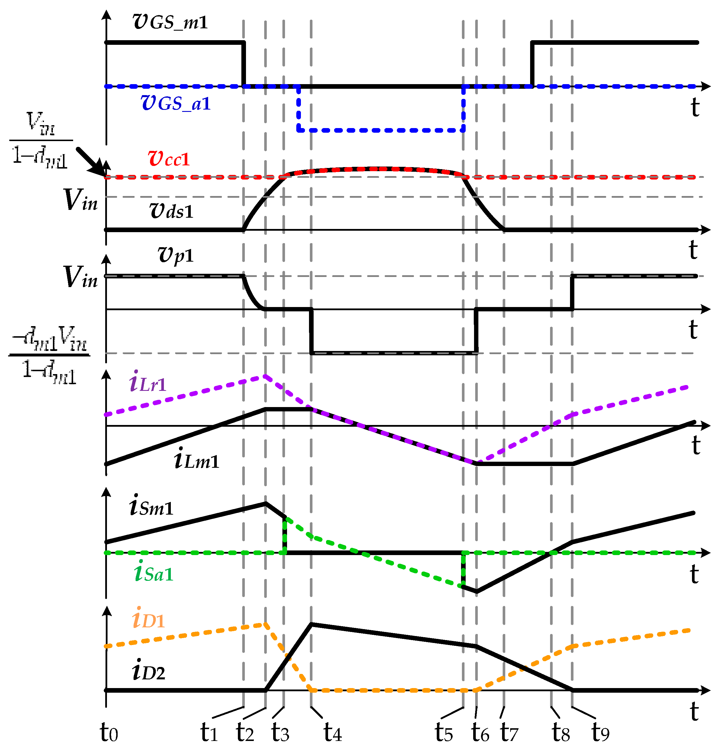
According to the state of the switching components and the direction of their currents, the operation of the active-clamp forward inverter can be divided into nine states in one high-frequency switching period. The theoretical timing diagram of each component is shown in
Figure 5, and the nine states will be described in order in the following. To simplify the circuit analysis, the following assumptions are made:
All components are ideal.
The clamp capacitor Cc1 is much larger than the parasitic capacitor Cds1 of the main power switch, and the magnetizing inductor Lm1 of the transformer is much larger than the leakage inductor Lr1.
The inductor L1 and the capacitor Cf are large enough so that the output voltage vo and the output current io can be regarded as constant in one switching period.
Because the dead time is extremely short, it can be ignored.
- A.
At the time
t =
t0, the main power switch
Sm1 is turned on, and the auxiliary switch
Sa1 is turned off. At this time, the primary voltage
vp1 across the transformer magnetizing inductor is equal to
Vin, so the current
iLm1 through magnetizing inductor rises linearly. The secondary voltage
vs1 of transformer is
Vin/
n, so the forward diode
D1 is forward biased, and the freewheel diode
D2 is reverse biased. The input power is transmitted to the inductor
L1 and the load
Ro via the transformer
Tx1 and the diode
D1. The equivalent circuit is as shown in
Figure 6a. The voltage
vds1 across the main switch
Sm1 and the current
iLr1 through the leakage inductor can be expressed as
where
ILo is the average current of the output inductor
Lo in one switching period. At the time
t =
t1, the main switch
Sm1 is switched off, and the circuit operation enters the next state.
- B.
When the main switch
Sm1 is switched off, the leakage inductor
Lr1, the magnetizing inductor
Lm1, and the parasitic capacitance
Cds1 are resonant in series. The current
iLr1 of leakage inductor starts to charge the capacitor
Cds1, the voltage
vds1 starts to rise, and the primary voltage
vp1 starts to drop. At this time, the forward diode
D1 remains on, and the freewheel diode
D2 remains off. The equivalent circuit of this state is as shown in
Figure 6b. The voltage
vds1 across the main switch and the current
iLr1 through the leakage inductor can be expressed as
where
, and
. The time the state 2 required can be expressed as follows:
At the time t = t2, vds1 rises to be equal to Vin, this state ends and goes to the next state.
- C.
At the time
t =
t2, the primary voltage
vp1 drops to be zero, so that both the forward diode
D1 and the freewheel diode
D2 are turned on. The forward diode current
iD1 is gradually reduced, and the freewheel diode current
iD2 is gradually increased. The equivalent circuit is shown in
Figure 6c. When the voltage
vds1 increases, the leakage inductor current
iLr1 decreases and can be expressed as:
The magnetizing current
iLm1 remains unchanged. At this time, the voltage
vds1 and the leakage inductor current
iLr1 can be respectively expressed as:
where
, and
. When the voltage
vds1 arrives
, the leakage inductor current
iLr1 stops charging the capacitor
Cds1, and the circuit operation enters the next state.
- D.
At the time
t =
t3, the leakage inductor current
iLr1 is charging the clamp capacitor
CC1 via the anti-parallel diode
Da1 of the auxiliary switch
Sa1, so the voltage across
Sa1 is zero. The equivalent circuit is shown in
Figure 6d. Since the anti-parallel diode
Da1 is turned on, the gate driving signal of the auxiliary switch
Sa1 must be provided during this state to achieve ZVS. At this time, the primary voltage
vp1 is zero. The clamp-capacitor voltage
vcc1 and the leakage inductor current
iLr1 can be expressed as
where
, and
. When
iLr1 is equal to
iLm1, the forward diode current
iD1 drops to zero, and this state ends.
- E.
At the time
t =
t4, since the forward diode current
iD1 is zero, the magnetizing inductor
Lm1 is in series with the leakage inductor
Lr1, and resonates with the clamping capacitor
Cc1. The primary voltage
vp1 is
, and the equivalent circuit is as shown in
Figure 6e. The leakage inductor current
iLr1 is equal to the magnetizing inductor current
iLm1 and continues decreasing. Due to the resonance, the direction of the current
iLm1 is reversed during this state, forcing the stored energy of the magnetizing inductor
Lm1 to be recycled to the input power source. In this state, the clamp-capacitor voltage
vcc1 and the leakage inductor current
iLr1 can be expressed as
where
, and
. This state ends when the driving signal of the auxiliary switch
Sa1 disappears.
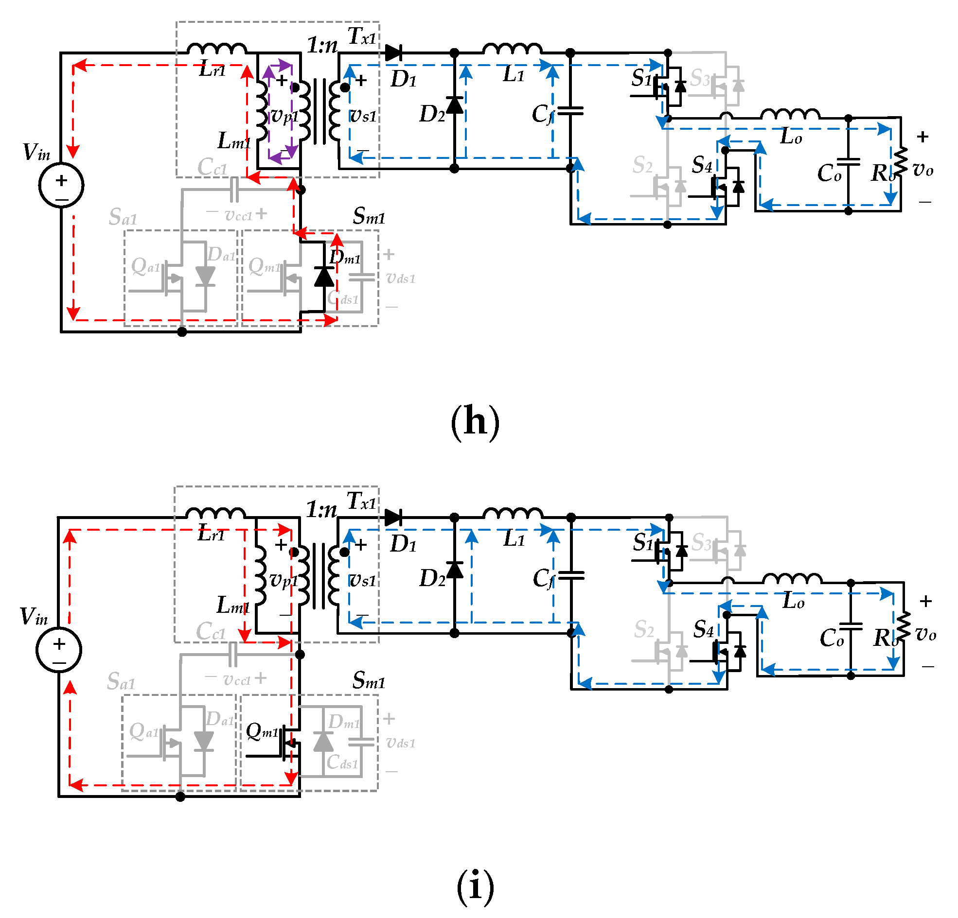
- F.
At the time
t =
t5, the auxiliary switch
Sa1 is turned off. The primary voltage
vp1 is
, so that the secondary voltage
vs1 is also negative. At this time, the resonant current flows through the capacitor
Cds1 to force it discharging, and the voltage
vds1 decreases. The equivalent circuit is as shown in
Figure 6f. In this state, the voltage
vds1 and the leakage inductor current
iLr1 can be expressed as:
where
, and
. This state ends when the voltage
vds1 drops to
Vin, and the time it takes is as follows:
- G.
At the time
t =
t6, the voltage
vds1 drops to
Vin, causing the primary voltage
vp1 equal to zero again. The magnetizing inductor
Lm1 no longer participates in resonance, and its current remains constant. The voltage across the leakage inductor
Lr1 is
Vin, so its current
iLr1 rises linearly from a negative value and with the slope of
Vin/Lr1. In addition, the forward diode
D1 is turned on again, so that the current
iD1 increases, and the freewheel diode current
iD2 decreases. The equivalent circuit is as shown in
Figure 6g. The voltage
vds1 across the main switch and the leakage inductor current
iLr1 are expressed as:
where
, and
. Since the direction of the current
iLr1 cannot be changed instantaneously, the anti-parallel diode
Dm1 is forced to turn on, and the energy is recovered to the input. In order for the main switch
Sm1 to have the ZVS characteristic, Equation (23) should satisfy
before this state ends. The following conditions can be obtained:
When the voltage
vds1 continues dropping to zero, this state ends and the time it takes is:
- H.
At the time
t =
t7, the current
iLr1 flows through the anti-parallel diode
Dm1 to release the energy stored in the magnetizing inductance
Lm1 back to the input power source, and the equivalent circuit is as shown in
Figure 6h. The driving signal of the main power switch
Sm1 should be applied in this interval. Since the anti-parallel diode
Dm1 has been turned on, the switch
Sm1 can achieve the characteristic of ZVS turn-on. Because the forward diode
D1 and the freewheel diode
D2 are remained being on state, the leakage inductor current
iLr1 continues to increase linearly with the slope of
Vin/Lr1, and can be expressed as:
When the current
iLr1 rises to be zero, this mode ends and the time it takes is:
- I.
At the time
t =
t8, the leakage inductor current
iLr1 becomes positive. The forward diode current
iD1 continues to increase linearly, and the freewheel diode current
iD2 continues to decrease linearly. The equivalent circuit is shown in
Figure 6i. In this state, the voltage
vds1 across the main switch and the leakage inductance current
iLr1 can be respectively expressed as:
When the diode
D2 is turned off at the time
t =
t9, the state ends, and one switching period of the proposed inverter is completed. The circuit operation will return to the state 1 of the next switching period, and the nine operation states are repeated in sequence. The time it takes for this stage is:
It can be seen from the above analyses that the advantages of the proposed inverter are listed as follows:
The magnetizing inductor current iLm1 of the transformer is bidirectional, so the iron core is operated in the first and third quadrants of the hysteresis curve, which can improve the core utilization.
Replacing the traditional reset winding, the auxiliary switch Sa1 and the clamp capacitor CC1 are used to reset the residual magnetic flux of the transformer. The energies of the magnetizing inductor and the clamp capacitor are mutually transferred so that the energy can be recycled to the input. Since both the magnetizing inductor and the clamping capacitor are passive components for energy storage, there is theoretically no power loss.
By using the magnetizing inductor and the leakage inductor of the transformer, both the main power switch Sm1 and the auxiliary switch Sa1 achieve the characteristics of ZVS turn-on, which can effectively reduce the switching loss.
5. Experimental Results
According to the foregoing analysis, a DSP-based prototype of the proposed inverter is built as an example for illustration. Refer to the circuit diagram shown in
Figure 7, the electrical specifications are listed in
Table 1.
Considering that the input voltage is 48 V and the peak output voltage
Vo,p is 156 V, the transformer turns ratio (
n) is selected as 10. From the transfer function of the forward converter, the duty ratio can be calculated as:
The boundary inductance
LB of
L1 in boundary conduction mode (BCM) can be derived as:
The inductor current is selected to operate in BCM under 20% load current and the peak of the output voltage. Therefore, the boundary inductance LB can be calculated from Equation (33) to be 2.57 mH. This boundary value is the minimum of output inductor L1, so the inductance of 3 mH is selected in the implementation example.
In this design, the magnetizing inductor
Lm1 of the transformer is 835 μH. From the operation principles mentioned before, the condition of that main switch
Sm1 achieves ZVS is:
where
. From Equation (23), the current
iLr1 (
t6) can be obtained as:
By combining Equations (34) and (35), the minimum value of the leakage inductance
Lr1 can be calculated as follows:
Choose 4 μH as the inductance of the leakage inductor Lr1.
Besides, the active-clamp forward inverter uses the auxiliary switch
Sa1 and the clamp capacitor
Cc1 to reset the residual magnetizing flux of the transformer. When the resonance of
Cc1,
Lr1 and
Lm1 occurs, the small value of
Cc1 will shorten the resonant period and induce voltage spikes. As a result, the voltage stresses of the clamp capacitor
Cc1, the main switch
Sm1, and the auxiliary switch
Sa1 are increased. Therefore, the resonant period should be designed to be greater than ten times the main switch turn-off time, that is:
From Equation (37), the capacitance of
Cc1 can be calculated as:
Choose 4 μF as the capacitance of the clamp capacitor Cc1.
According to the previous design and calculations, the selected component parameters are summarized in
Table 2. The experimental results described below will be used to verify the feasibility of the proposed circuit architecture and the correctness of the theoretical analysis.
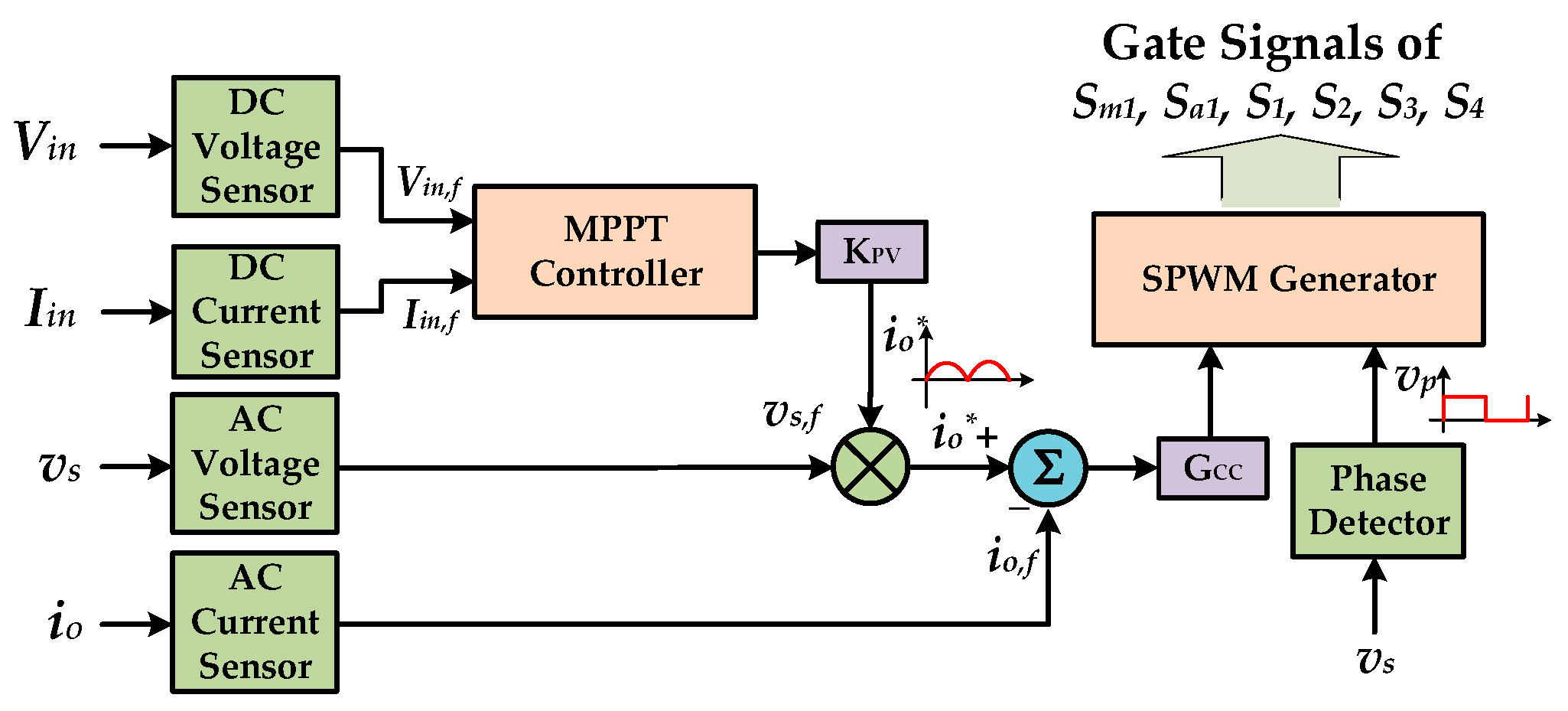
The proposed active-clamp forward inverter is driven by SPWM signals.
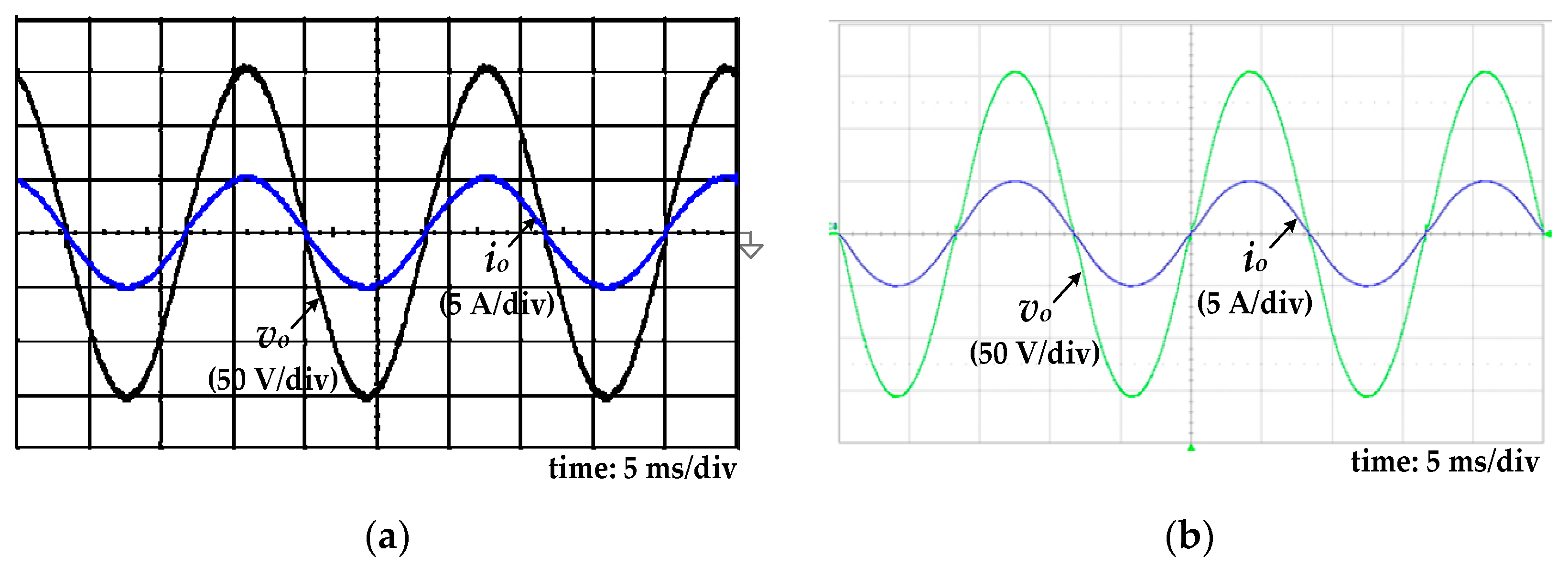
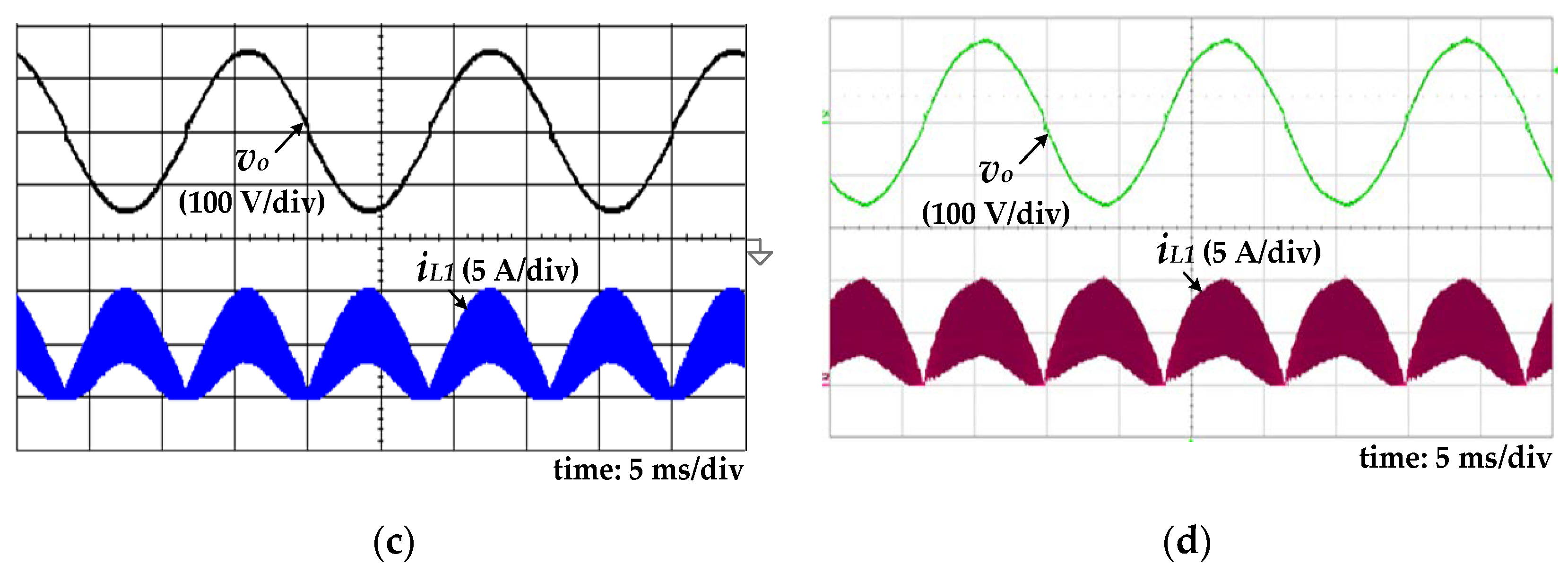
Figure 9a,b are the simulation and measured waveforms of the output voltage
vo and output current
io when the inverter is operated at 48 V input voltage, and
Figure 9c,d are the simulation and measured waveforms of the output voltage
vo and output inductor current
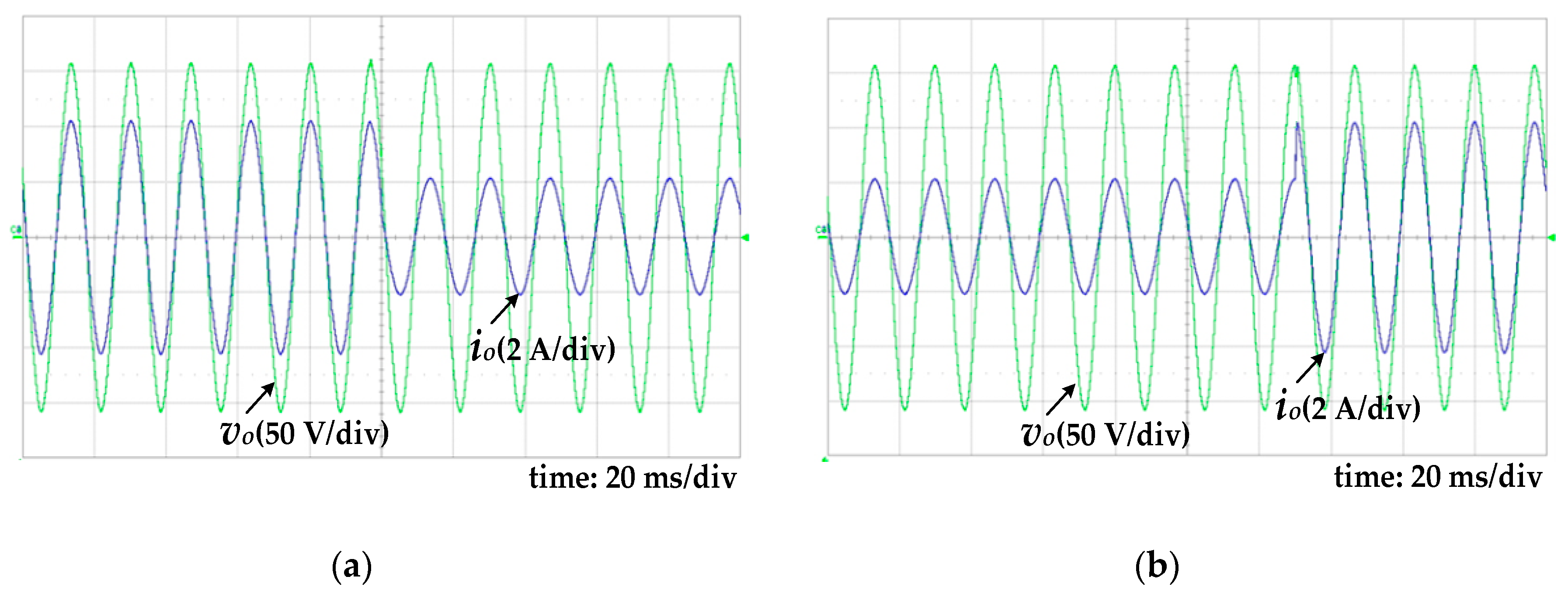
iL1. It can be seen from the figures that the output voltage and current are in the form of a sine wave with low distortion, which proves that this isolated inverter can effectively convert the DC voltage into an AC output. Furthermore,
Figure 10 shows the measured waveforms of the output voltage
vo and output current
io when the inverter operates with the step load change between 320 W and 160 W. As can be seen, the output voltage can be quickly and stably regulated to a sine wave of 110 V
rms, proving that the proposed inverter has good dynamic voltage regulation capability. In addition, the line regulation is 1.26%, and the load regulation is 0.78%, which meets the general specifications of ±3%.
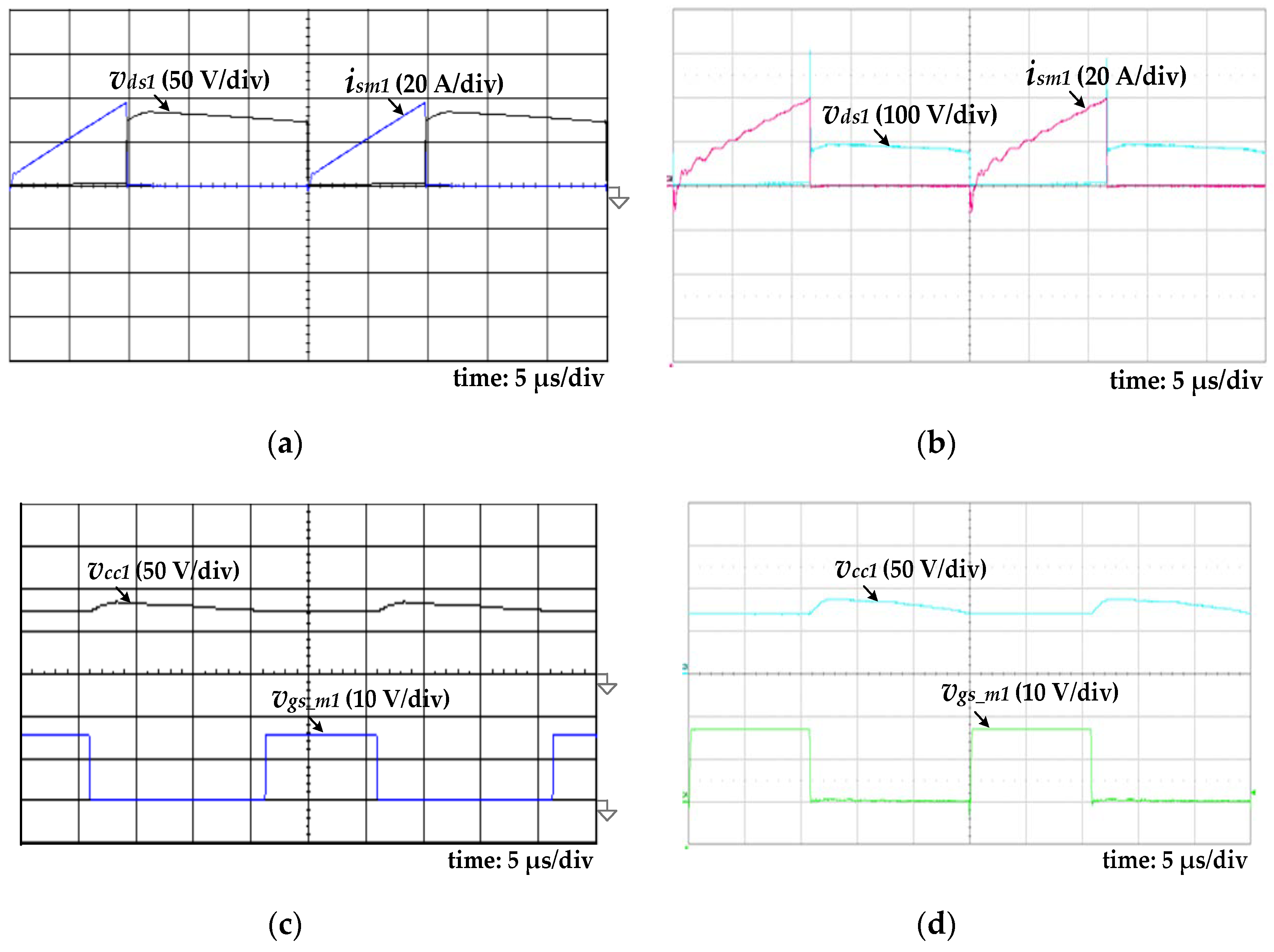
Figure 11 shows the simulation and measured waveforms of the main-switch voltage
vds1, the main-switch current
ism1, and the clamp-capacitor voltage
vcc1, when the inverter is operated at 48 V input voltage and the full load of 400 W. Since the resonant current flows through the anti-parallel diode
Dm1 before the main switch
Sm1 is turned on, it can be seen from
Figure 11a,b that the main switch
Sm1 can achieve the characteristics of ZVS turn-on, which can effectively reduce switching loss. In addition, it can be seen from
Figure 11c,d that the maximum value of the clamp-capacitor voltage
vcc1 is about 95 V, which can effectively limit the voltage stress of the main power switch
Sm1. Therefore, the power MOSFET with lower voltage rating and lower on-resistance can be selected to reduce conduction loss.
Table 3 shows the total harmonic distortion (THD) and odd-order harmonics of the output voltage
vo when the inverter is operated at 48 V and 72 V input voltages. The results meet the requirements of electrical standards and verify the correctness of the theoretical analysis again.
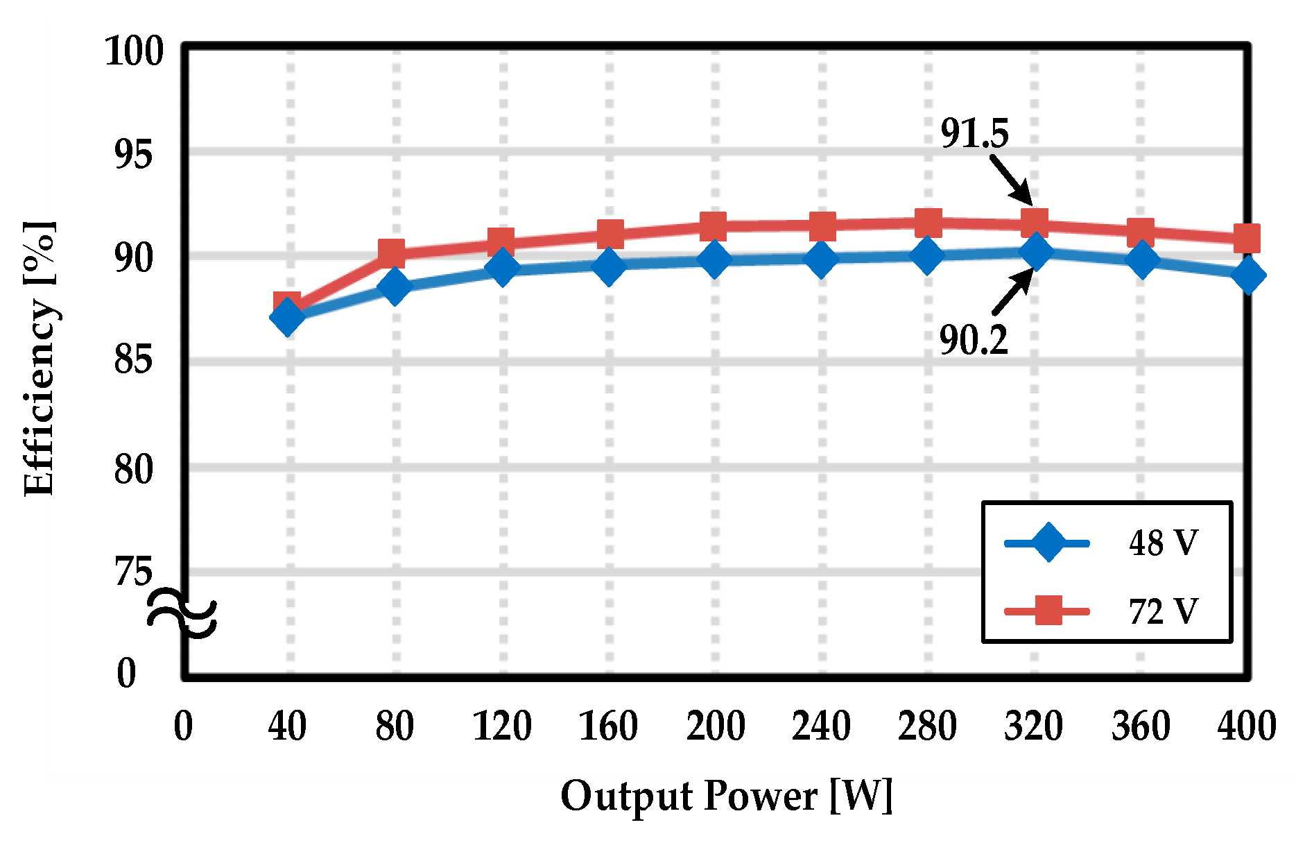
Figure 12 shows the measured efficiency curve of the active-clamp forward inverter. The highest efficiency is 90.2% at 48 V input and 91.5% at 72 V input, respectively.
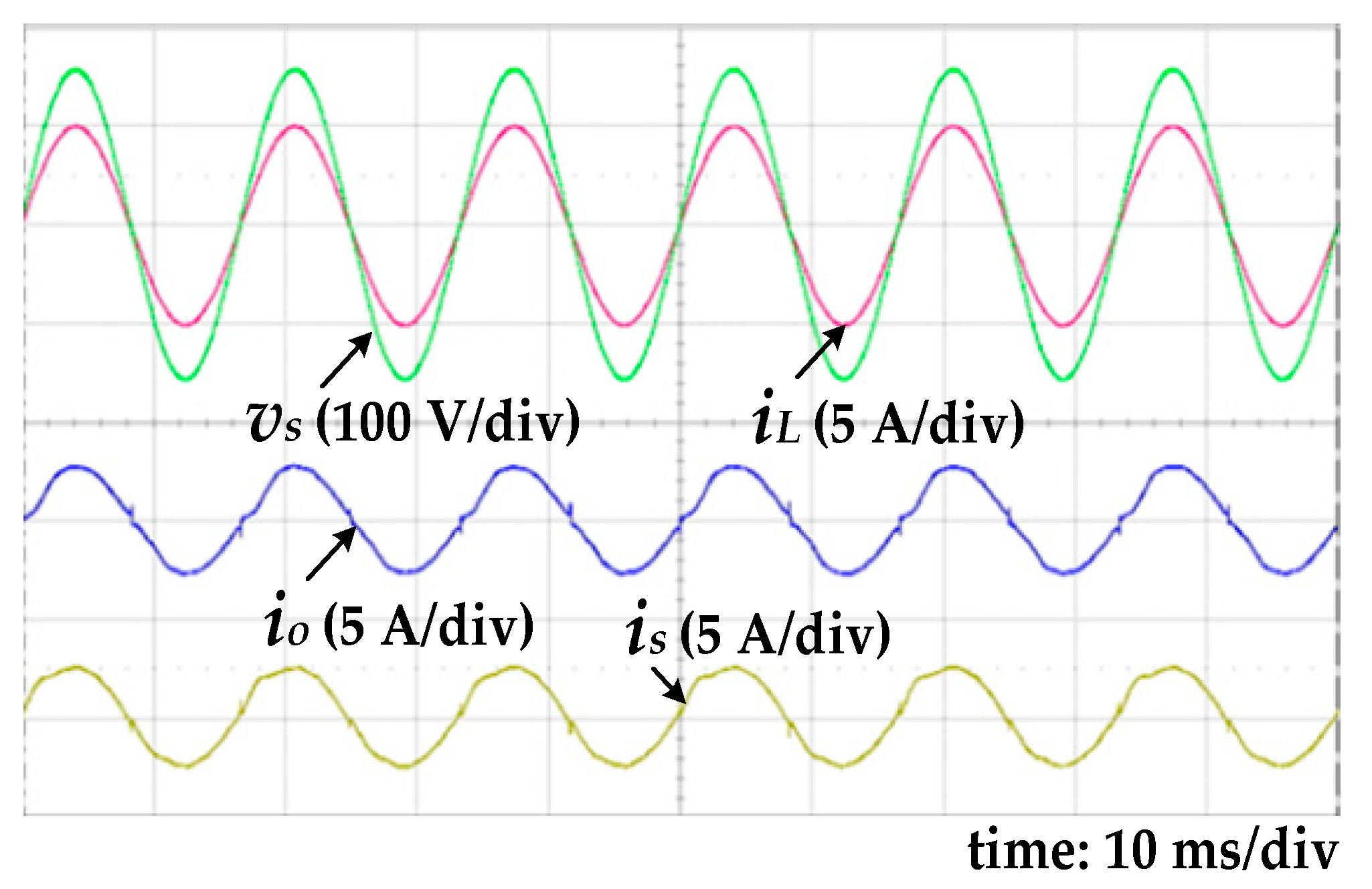
Furthermore,
Figure 13 shows the measured waveforms of the load current
iL, the inverter output current
io, the utility-line current
is and the utility-line voltage
vs, under the operation of grid-connection mode. In this case, the inverter output current
io is controlled to follow the frequency and the phase of the utility-line voltage
vs. In this way, the power of the PV panel can be delivered to the load and the utility-line by the proposed active-clamp forward inverter. It can be clearly seen from
Figure 13 that the output current is close to an ideal sine wave and in phase with the utility-line voltage. At this condition, the inverter outputs about 200 W of power, and utility-line provides approximately 200 W of power to meet the total power requirement of the load. It can prove the feasibility of grid-connection of the proposed inverter. In addition, the power factor, the THD and odd-order harmonics of the output current are measured and recorded in
Table 4. Either the THD or each harmonic can meet the specification requirements, and the power factor reaches 0.994. This further confirms the feasibility of the circuit structure and control strategy mentioned in this paper.
Many pseudo-dc-link inverters based on forward converters are proposed to improve conversion efficiency and to achieve electrical isolation [
20,
21]. In order to compare the difference between them and the proposed forward inverter in this paper, a brief discussion is presented as follows according to (1) the reset circuit for residual magnetic flux, (2) the conversion efficiency, (3) the characteristic of switch, and (4) the circuit complexity.
- (1)
Reset circuit for residual magnetic flux
The forward inverter in Reference [
20] needs a third winding in series with a diode to reset the residual magnetic flux. Therefore, the maximum duty ratio is limited, resulting in a reduction of boosting capacity. The dual-switch forward inverter in Reference [
21] adds an additional power switch and a diode to reset the residual magnetic flux. Since the input current goes through these devices, the volume and cost are greatly increased. In the proposed active-clamp forward inverter, an auxiliary switch and a clamp capacitor are used to reset the residual magnetic flux through the resonance of the clamp capacitor and the magnetizing inductor, which can avoid the problems mentioned above.
- (2)
Conversion efficiency
According to the efficiency curve shown in
Figure 12, the efficiency of the active-clamp forward inverter is up to 90.2% at 48 V input and 400 W output power. The measured efficiency of the forward inverter in Reference [
20] is 89.5% at 45 V input and 110 W. Besides, the measured efficiency of the dual-switch forward inverter in Reference [
21] is only 82% at full load. Therefore, it can be concluded that the proposed inverter has better conversion efficiency than other forward inverters.
- (3)
Characteristic of switch
In the proposed active-clamp forward inverter, both of the main switch and the auxiliary switch have the characteristic of ZVS turn-on. In addition to reducing switching losses, switching noise can also be reduced to avoid electromagnetic interference (EMI) problems. For the forward inverters proposed in References [
20,
21], the power switches are hard switching, which may increase switching loss and cause serious EMI issues.
- (4)
Circuit complexity
In order to reduce the core size of the transformer, multiple converters with interleaved parallel connections are used in the forward inverter in Reference [
20]. Although the efficiency is improved slightly, the circuit complexity and cost are increased significantly. Besides, two dual-switch forward converters are parallel connected in the inverter of Reference [
21], and each secondary side of the transformer is center tap, resulting in high circuit complexity. The proposed inverter uses only a single active-clamp forward converter and does not need to add a third winding, so its circuit architecture is much simpler than other forward inverters.


