Article

Structure and Properties of High-Strength Cu-7.7Nb Composite Wires under Various Steps of Strain and Annealing Modes

by
Irina L. Deryagina
*,
Elena N. Popova
* and
Evgeny I. Patrakov
M.N. Miheev Institute of Metal Physics, Ural Branch of Russian Academy of Sciences, 620108 Ekaterinburg, Russia
*
Authors to whom correspondence should be addressed.
Metals 2023, 13(9), 1576; https://doi.org/10.3390/met13091576
Submission received: 8 August 2023 / Revised: 28 August 2023 / Accepted: 7 September 2023 / Published: 9 September 2023
(This article belongs to the Special Issue Feature Papers in Metal Matrix Composites)

Abstract

:
Microstructure and mechanical properties of in situ Cu-7.7Nb microcomposite (MC) wires manufactured by cold drawing with intermediate heat treatment (HT) have been studied. The evolution of Nb filaments morphology under various steps of deformation and modes of intermediate HT have been studied by the SEM and TEM methods. According to X-ray analysis, internal microstresses accumulate in the niobium filaments of the drawn MC, leading to a decrease in ductility. After heat treatment, the ductility of the wire increases significantly, since the microstresses in the niobium decrease even at the lowest HT temperature. The strength of the composite decreases under the HT because of negative changes in morphology and interface density of Nb filaments. The <110>Nb texture is stable under the HT up to 800 °C. The Nb filaments morphology and semi-coherent boundaries at Cu/Nb interfaces are restored under the post-HT cold drawing, leading to a sharp increase in the strength of the MC wire. Reducing the niobium concentration to 7.7%Nb relative to the traditional MC with 16–20%Nb and the recovery of the wire ductility under the HT makes it possible to obtain long-scale high-strength microwires with an extremely small diameter of 0.05 mm and high ultimate tensile strength of 1227 MPa.

1. Introduction

Various types of composite materials are presently studied to meet the growing requirements of modern industries [1,2,3,4]. As a rule, these materials should demonstrate a combination of enhanced properties, such as strength, ductility, durability, corrosion resistance, etc. [5,6]. In the design of high-strength Cu-based alloys, the main problem is to ensure high strength without losing ductility, because the movement of dislocations promoting high ductility is hindered by internal obstacles (grain boundaries, second phase particles) ensuring high strength. Modern electronics involves the requirements of miniaturization, complexity and reliability of integrated circuits [7].
A special class of composites attracting great attention from materials science researchers are two-phase composite wires based on FCC copper matrix with an addition of BCC metals such as Fe, Cr, V and Nb, which demonstrate high strength along with high electrical conductivity [8]. In this series, Cu-Nb composites are favorites, since their ultimate tensile strength (UTS) can reach 2000 MPa (at 77 K), and the electrical conductivity remains at a level of up to 82% of the electrical conductivity of pure copper, according to IACS (International Annealed Copper Standard for annealed copper with electrical resistivity 1.7241 μΩ·cm) [8]. Cu-Nb microcomposite (MC) wires with high UTS are required for operation under extremely high mechanical loads, for example, as contact wires for high-speed trains of railway transport and winding wires for high-field pulsed magnets [8,9,10,11,12,13]. The reinforcement of Nb3Sn-based superconducting wires with the Cu-18Nb inserts led to a more uniform deformation of the wires under drawing and, as a consequence, to an increase in their current carrying capacity [14,15].
Cu-Nb billets for MC wires are obtained by the bundle and deform, and by the melt-and-deform (the so-called, in situ) processes [11]. In the latter, nano-sized niobium filaments are formed from Nb dendrites in a Cu matrix under drawing of a Cu-Nb billet obtained by melting. For the fabrication of MCs, initial Cu-Nb billets are subjected to large plastic deformation by multistage processes of extrusion followed by cold drawing or rolling. At true strains of η > 6 (where η = ln A0/A, A0 and A being the cross-sectional areas of a composite before and after deformation), the UTS of a Cu-Nb wire exceeds the UTS of a copper–niobium composite calculated according to the rule of mixtures [11]. Such changes in strength indicate the beginning of the microcomposite formation when a certain relationship is established between crystal lattices of copper and niobium in the Cu/Nb interfaces. For an achievement of extremely high strength (up to 2000 MPa) in the in situ produced Cu-Nb MCs the heavy cold deformation with η of about 11 and higher is required. Hence, to produce high-strength wires with a diameter of 0.1–0.4 mm the initial billets of 70–100 mm in diameter are used [16].
Note that in MCs, the interface area between the matrix and the reinforcing filaments plays an extremely important role. It is known that two-phase composites based on BCC-FCC crystal lattices (Cu-Fe, Cu-Cr, Cu-V, Cu-Nb) have higher strength than composites based on FCC-FCC lattices (Ag-Ni, Cu-Ag) [8]. This difference is explained by more branched interfaces between the components of BCC-FCC composites and, accordingly, higher interface density compared to FCC-FCC composites. Under deformation, the FCC filaments in the FCC matrix are reduced in diameter, but their shape does not change, retaining a rounded cross-section. In contrast, under heavy drawing of bimetallic composites with FCC matrix and BCC second component, the morphological transformation of the BCC metal occurs, and its grains take the form of ribbon-like filaments uniformly distributed in the FCC matrix.
In the Cu-Nb MC, thin ribbon-like niobium filaments are formed in the copper matrix of the wire under high strain. These Nb-ribbons are elongated along the axis of the wire, and have a complex curved shape in transverse sections [8,11,17,18]. Under drawing a sharp axial texture <110>Nb is formed in niobium filaments, and a double axial texture with a strong <111>Cu and a weak <100>Cu components is formed in the copper matrix [19]. It is known that in the high-strength Cu-Nb MC, the boundaries between the copper and niobium grains at Cu/Nb interfaces are semi-coherent and, in some areas, even amorphous [8,20,21,22,23,24,25]. In the case of semi-coherent boundaries, the misorientation angle between (111)Cu and (110)Nb crystallographic planes is about 4–5 degrees. Note that interfaces in two-phase MCs are of great importance because their high strength depends on the area of the interface, which increases with strain [11,20,21,23,26].
The state of the Cu/Nb interfaces can be affected by the so-called grain boundary wetting, which is observed in multiphase objects not only in the liquid but also in the solid state [27]. The wetting of Cu/Cu boundaries was observed in Cu-Co and Cu-Ag alloys [28]. The presence of the grain boundary wetting phase strongly affects the mechanical and other properties of multiphase objects [29]. In the Nb3Sn-based superconducting composites produced by the bundle-and-deform method, this phenomenon was also observed, namely, in the vicinity of Cu/Nb interfaces the Nb grains were wetted by Cu phase, and their boundaries were rugged and comb-like [30]. However, no signs of wetting were reported in in situ Cu-Nb composites.
Along with high strength of not less importance for practical application of Cu/Nb MCs is their high electrical conductivity, which is ensured by an extremely low mutual solubility of Cu and Nb, which is 0.15–0.20% Nb in Cu and 0.4–0.5% Cu in Nb [31]. A great difference in melting temperatures (1356 K for Cu and 2740 K for Nb) and an absence of intermediate intermetallic compounds make these two elements the best candidates for the in situ fabrication of MC wires. Only under the high-pressure torsion (HPT), the mutual solubility of Cu and Nb increases to 1.5 at % Nb in Cu and 10 at % Cu in Nb, but, nevertheless, both phases are retained in contrast to the Cu–Fe composite, in which a supersaturated solid solution of Fe in copper is formed [32,33,34].
A specific feature of MCs studied in this research is the reduced to 7.7 wt.% concentration of niobium, in contrast to traditional Cu-Nb composites with niobium concentration 16–18 wt.% [11,16,17,19,20]. Reducing the niobium concentration makes it possible to increase the wire ductility in order to produce the so-called microwires of small diameter with high conductivity and high strength. In the last few years, the need for high-strength microwires has sharply increased in a number of branches of industry, such as aerospace engineering, microelectronics and computer technology. However, as the concentration of niobium in the Cu-Nb MC decreases, an increase in strain is required to achieve high strength. Thus, to achieve the UTS of 1200 MPa, a deformation with η ≈ 7 for Cu-16%Nb wire and with η ≈ 13 for Cu-8%Nb wire is required [35]. With an increase in deformation, microstresses accumulate in composite wires, which reduces their ductility and leads to the rupture of MC wire under drawing. In addition, it is known that with an increase in deformation, the electrical resistance of two-phase MCs increases due to an increase in the number of structural defects [35,36,37]. To minimize these negative factors, intermediate heat treatments are required.
The goal of this research is to study the effect of strain and intermediate HT on the strength, ductility and structure of Cu-Nb MCs with reduced to 7.7 wt.% concentration of niobium. In this work, for the first time, the evolution of the structure of Nb filaments of this composite is presented in detail depending on strain and annealing regimes. Based on the results of this study, the authors will show what structural changes affect the strength and ductility of this composite. The results of the study will help to justify the choice of the optimal intermediate annealing temperature for the achievement of the best combination of mechanical properties, and demonstrate which changes in the structure of the composite have the greatest effect on its strength and plastic characteristics.

2. Materials and Methods

The Cu-7.7Nb in situ composites were produced by the Research and Production Company (RPC) “NANOELECTRO”. The initial composite billets for MC wires were obtained by the method of vacuum arc melting (in situ method) with a consumable electrode. The initial content of niobium in the charge was calculated as 7.7 wt.%. To fabricate the composite wires, high-pure niobium (99.9%) and high-pure oxygen-free copper (99.99%), obtained by electron beam melting were used. The melted ingot of the Cu-7.7Nb composite was placed in a copper tube and extruded at a temperature of 750 °C–800 °C to a diameter of 45 mm. Then, the Cu-clad Cu-7.7Nb billet was subjected to multistep cold drawing to a diameter of 0.05 mm with intermediate HT on the diameter of 2.54 mm. The intermediate HT was carried out in three modes: 550 °C, 1 h; 700 °C, 1 h; and 800 °C, 1 h. In this study, we investigated samples with varying true strain, from η = 3.21 (wire diameter of 9.02 mm) to η = 13.6 (wire diameter of 0.05 mm).
The mechanical properties of the wires were measured in the RPC “NANOELECTRO”. Tensile tests of composite wires were carried out on samples of 200 mm in length on the Instron TT-DM testing machine at room temperature with an accuracy of ±10 MPa.
For scanning electron microscopy (SEM) polished transverse and longitudinal sections of the samples were used. SEM images were obtained in SEM Inspect-F (FEI) at an accelerating voltage of 20 kV in the mode of secondary electrons.
Transmission electron microscopy (TEM) was performed on a JEM-200CX (JEOL) microscope on the foils of longitudinal and transverse sections of composite wire samples. Mechanically thinned foils for TEM studies were polished in a mixture of acids (3 HNO3: 2 H2SO4: 1 HF).
The calculations of average values of the perimeter, area, aspect ratio and interface density of niobium filaments were carried out based on SEM images of transverse sections of the samples. The specially written program for statistical image analysis of inclusions (in our case, Nb filaments in Cu matrix) calculates the perimeter (Cu/Nb interface) and area of all inclusions in an SEM image. The main steps of the program are as follows. Firstly, the program converts the analyzed SEM image to the grayscale mode and then binarizes the image. Then, the program marks the boundaries of niobium filaments in the binarized SEM image with red color (Figure 1a). The number of all red pixels corresponds to a perimeter in pixel units of all Nb filaments in the image. By filling with red the entire cross-section of the Nb filaments (Figure 1b), the program calculates the cross-sectional area (in pixels) of all Nb filaments in the SEM image. The average interface lav and average filament area are calculated by dividing the total filaments interface or total filaments area in the SEM image by the total number of filaments in this image, respectively. Then, the program converts the results of the analysis in pixels into microns or nanometers, using the scale bar of the SEM image. Based on the ratio of the perimeter to the area of the inclusions, the program calculates the aspect ratio (AsR) of Nb filaments using the standard method of an equivalent rectangle. Recall that an equivalent rectangle is a rectangle, whose area is equal to the area of the analyzed element (in our case, the cross-section of Nb filaments).
The X-ray diffraction analysis (XRD) of the Cu-Nb composites was carried out by the Empyrean (Panalytical) and DMAX-2200 (Rigaku) diffractometers with Cu Kα radiation. The angle interval of 2Θ scanning was 30–140 degrees, the step of scanning was 0.02° and the scan time was 0.4 s at a point. The calculation of the crystal lattice parameters was carried out using the HighScore Plus 4.1 software package. The microstresses in Nb filaments and Cu matrix were calculated by the conventional Williamson–Hall method from the diffraction peaks broadening FWHM (full width at half maximum) with the help of the JADE 6.0 software package as:
μ = F W S cos θ 4 sin θ 100 %
where µ is a microstress, FW(S) is an X-ray peak broadening by a sample, which is calculated as the difference between the FWHM (full width at half maximum) of the peak and an instrumental broadening, Θ is Bragg angle in radians.

3. Results and Discussion

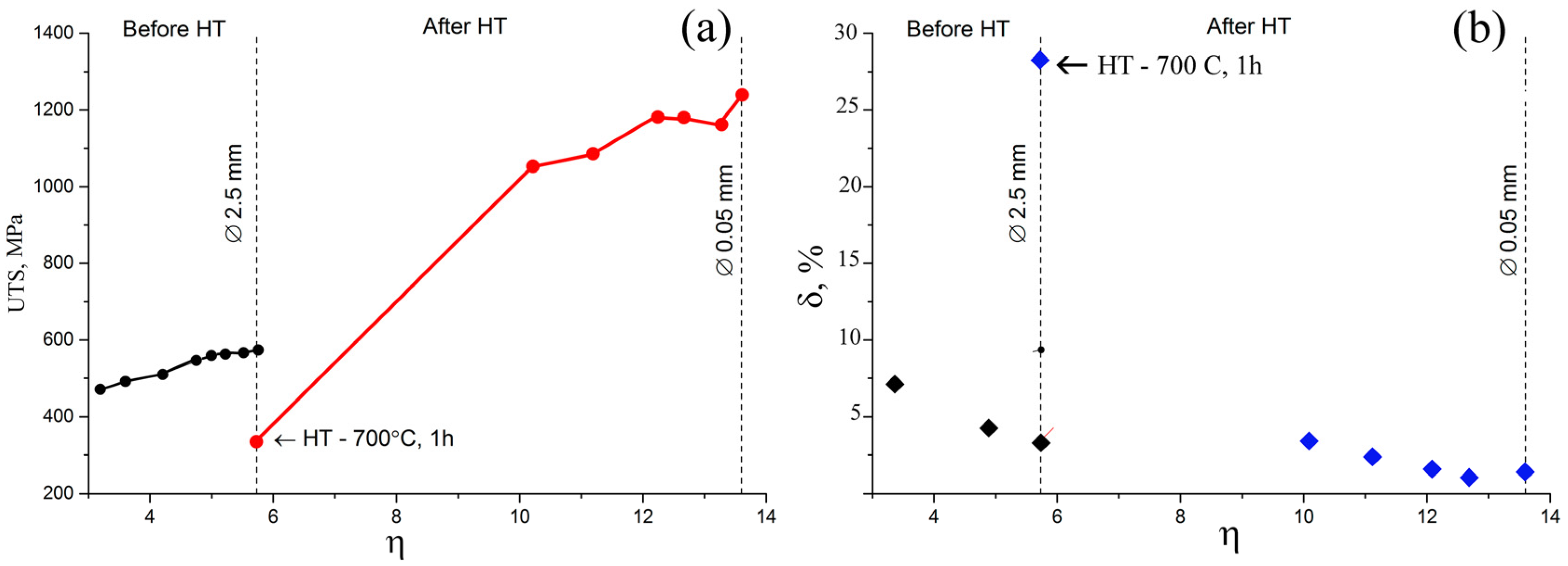
3.1. Mechanical Properties before and after HT

The main parameters of the studied samples at various steps of cold drawing before and after intermediate HT at different temperatures are presented in Table 1.
With the true strain increasing from η = 3.21 to η = 5.74 under the wire cold drawing from a diameter of 9.02 mm (sample #1) to 2.54 mm (sample #3), its strength (UTS in Table 1) increases from 470 MPa to 574 MPa, and ductility (relative elongation δ in Table 1) decreases by a factor of two. Such a strong decrease in the plasticity of the wire indicates its work hardening and the need for intermediate annealing at this stage of drawing.
Three intermediate annealing temperatures 550 °C, 700 °C and 800 °C were tested on samples with a diameter of 2.54 mm (samples #4-0, #5-0 and #6-0). All three HT modes lead to a remarkable increase in the ductility of the wire. At the same time, all three HT modes lead to a decrease in strength. The UTS of samples #4-0, #5-0 and #6-0 decreases with an increase in HT temperature by 34%, 41% and 47%, respectively, compared to sample #3-0 of the wire before HT. However, the cold drawing of the heat-treated wires to the diameter of 0.27 mm leads not only to restoration, but to a sharp increase in the strength of the wire to UTS of about 1000 MPa (sample #6-1) and higher (samples #4-1, #5-1). Due to the restoration of the Cu-Nb wire ductility under the HT, and the increase in its strength under subsequent deformation, the microwires with a diameter of 0.05 mm and UTS of about 1200 MPa were obtained (samples #4-2, #5-2 and #6-2).
The strength of compositional and other materials is affected by a number of parameters, and first a all by the presence of dislocations in grain bulk and boundaries. The development of high-strength materials assumes two ways: by the creation of microstructures without dislocations (for example, the so-called whiskers), or by an increase in the amount of different obstacles that effectively block the dislocation motion [8]. In the MCs, the internal interphase surface plays the role of a barrier for dislocation motion, and the high density of interfaces leads to the high strength of composite materials. According to Ref. [16], an intensive drop of strength in the Cu-Nb composite under the heat treatment at about 400 °C and higher is associated with transformation in the dislocation structure of niobium grains.
To reveal what changes in the structure of the Cu-Nb composite affected its strength and plastic characteristics before and after HT, the samples of MC wires presented in Table 1 were studied using XRD, SEM and TEM methods.

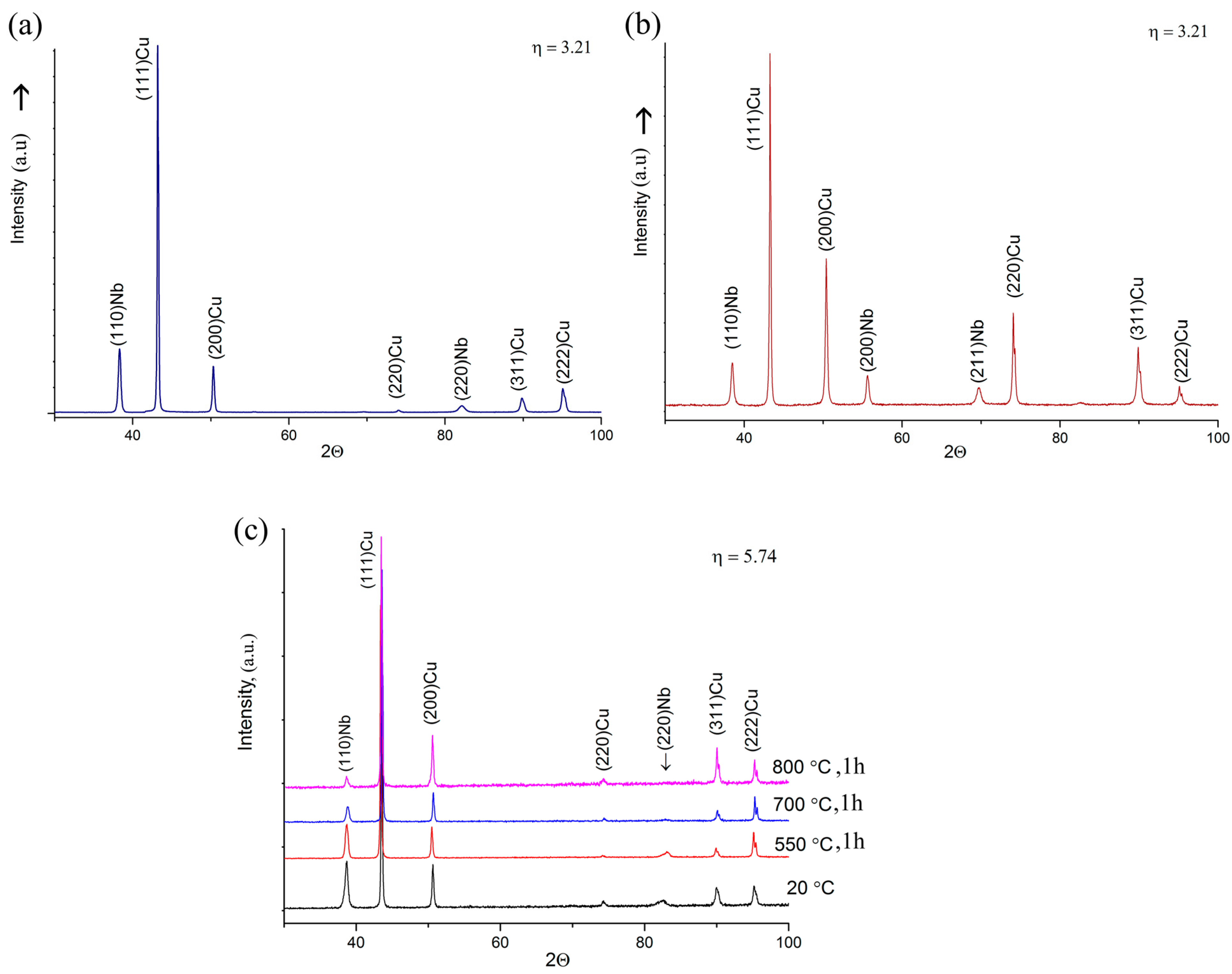
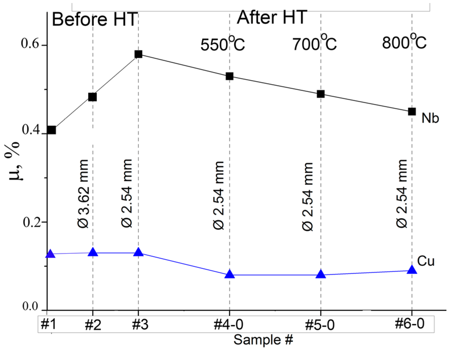
3.2. Texture and Internal Stresses

X-ray diffraction analysis (XRD) was carried out on the transverse and longitudinal sections of sample #1 with a diameter of 9.02 mm (Figure 2a,b) and transverse sections of the samples with a diameter of 2.54 mm (Figure 2c) before HT (sample #3) and after HT (samples #4-0, 5-0 and #6-0).
As the XRD pattern from the longitudinal section of sample #1 contains all main peaks of the Nb and Cu characteristic X-ray spectra, the lattice parameters were calculated from this spectrum (Figure 2b). According to the calculation, the composite wire consists of two phases: copper with the Fm3m symmetry and the FCC lattice parameter a = 3.6155 Å and niobium with the Im3m symmetry and the BCC lattice parameter a = 3.3015 Å. The XRD analysis of transverse sections of the samples (Figure 2a,c) showed the presence of an axial drawing texture with the axes <110>Nb ‖ <111>Cu ‖ DA (drawing axis) in niobium filaments and copper matrix, which is characteristic of binary composites based on the FCC matrix and the second component with a BCC lattice. The XRD data also demonstrate a weak additional texture <100>Cu, which is always present both in pure copper wire [38] and in the copper matrix of Cu-Nb composite wires [17,39]. The presence of weak (220) Cu and (311) Cu peaks in the XRD patterns of the transverse sections indicates the inhomogeneity of texture over the wire section. Such inhomogeneity is characterized by a deviation of <111>Cu texture axis at the wire periphery from the drawing axis by 15–25 degrees [38].
The texture of niobium <110> Nb ‖ DA is complete before HT and does not change after the HT. The XRD patterns of samples #1 (Figure 2a) and #3 (Figure 2c) contain niobium peaks only from the {110}Nb lattice planes. It is known that in Cu-Nb drawn MCs with 16–20% of niobium, the <110>Nb texture is formed under the strain η ≥ 4 [39]. In the samples of composite with 7.7% Nb under study, the <110>Nb texture is completely formed at the true strain η = 3.2 (sample #1). It is known also that in heavily deformed MCs (η ≥ 10) with 18%Nb, the <110>Nb texture is resistant to annealing at 400 °C- 800 °C [19,40]. In the samples with 7.7% Nb and η = 5.74, the <110>Nb texture is resistant to all the tested annealing temperatures up to 800 °C (Figure 2c). The relative intensity I* of (110)Nb peak is 100% for all the heat-treated samples (Table 2). Note that the main texture of copper <111>Cu is less resistant to annealing, since after the HT at 700 °C and 800 °C, the relative intensity I* of the (111)Cu peak is somewhat decreased (Table 2).
Internal microstresses (µ) accumulated under deformation in the Cu matrix of the samples before HT (samples #1, #2 and #3 in Table 2 and Figure 3) are low and not sensitive to deformation, which results from the ability of copper to dynamically recover and recrystallize under drawing. Microstresses in niobium filaments are much higher and they increase with strain. The intermediate HT reduces the microstresses in niobium (Table 2, Figure 3), and, as a result, the ductility of the heat-treated wires (δ in Table 1) increases, creating conditions for further deformation of the composite wire.
The parameter Δ in Table 2 characterizes the mismatch between the (110)Nb and (111)Cu crystallographic planes at the Cu/Nb interface, which is calculated by the formula:
Δ = d 110 N b d 111 C u d 110 N b 100 % ,
where dNb110 and dCu111 are the interplanar spacing for the (110) niobium and (111) copper crystallographic lattices.
Even in early studies of Cu-Nb composites, it was shown that at high strains the mismatch between (111)Cu and (110)Nb planes increases, which results in the formation of periodic mismatch dislocations at Cu/Nb interfaces and, consequently, to semi-coherent bonds between Cu matrix and Nb filaments, leading to a sharp increase in composite strength [21,41]. The parameter Δ for non-deformed niobium and copper is 10.6% [11]. In heavily deformed Cu-Nb composites with η ≥ 9.64, the Δ increases to 12.5% [11,19]. Under annealing of heavily deformed composites, the parameter Δ decreases down to its initial values [19,42]. The parameter Δ of samples #1–#3 is about 10.6 (± 0.1) and does not change under the heat treatment (samples #4-0, #5-0 and #6-0 in Table 2). Hence, it may be suggested that in the wires with η ≤ 5.74, the semi-coherent bonds on the Cu/Nb interfaces have either not formed, or are at the initial stage of formation.
As noted above, intermediate annealing reduces the microstresses in niobium and sharply increases the ductility of the wire. At the same time, the strength of heat-treated samples is markedly reduced (UTS in Table 1). For example, the UTS of sample #3 (η = 5.74) reduces from 574 MPa before HT to 308 MPa after HT at 800 °C (sample # 6-0), approaching the UTS of 300-308 MPa in niobium with η of about 0.5 [39]. The decrease in the strength of composite wires may be associated with changes in their microstructure. Indeed, Figure 4 demonstrates that the morphology of niobium ribbons etched out of the copper matrix strongly differs in the samples before and after HT. Before the HT, niobium filaments look like elongated thin ribbons with smooth surfaces semitransparent for the electron beam of SEM (Figure 4a). After HT at 700 °C, Nb filaments thicken and some of them take the shape of cylindrical rods due to coagulation (Figure 4b). After HT at 800 °C, they become thicker and acquire a bamboo-like shape with numerous constrictions (Figure 4c). Since it is known that the strengthening of MC with an increasing strain is associated with a decrease in the Nb filaments thickness and an increase in the perimeter of the interfaces between Nb filaments and copper matrix, the changes in the niobium filaments morphology in the samples before and after HT are considered in more detail in the next section.

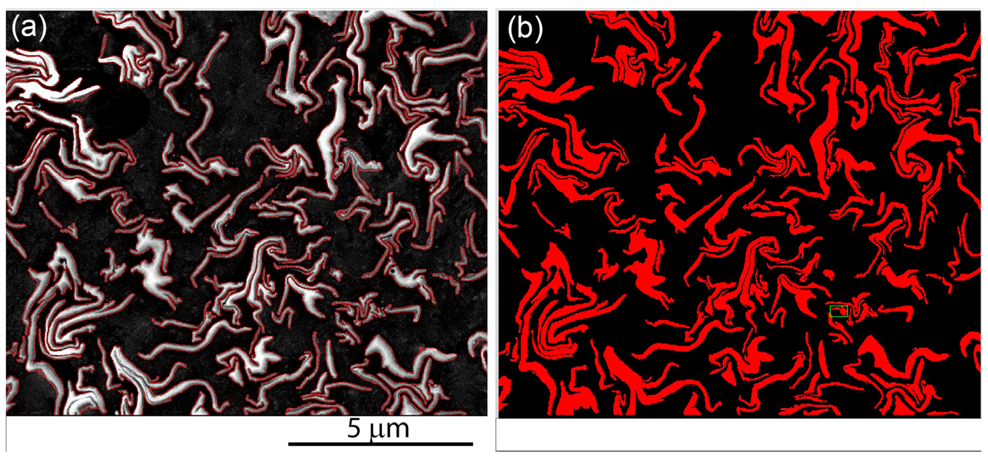
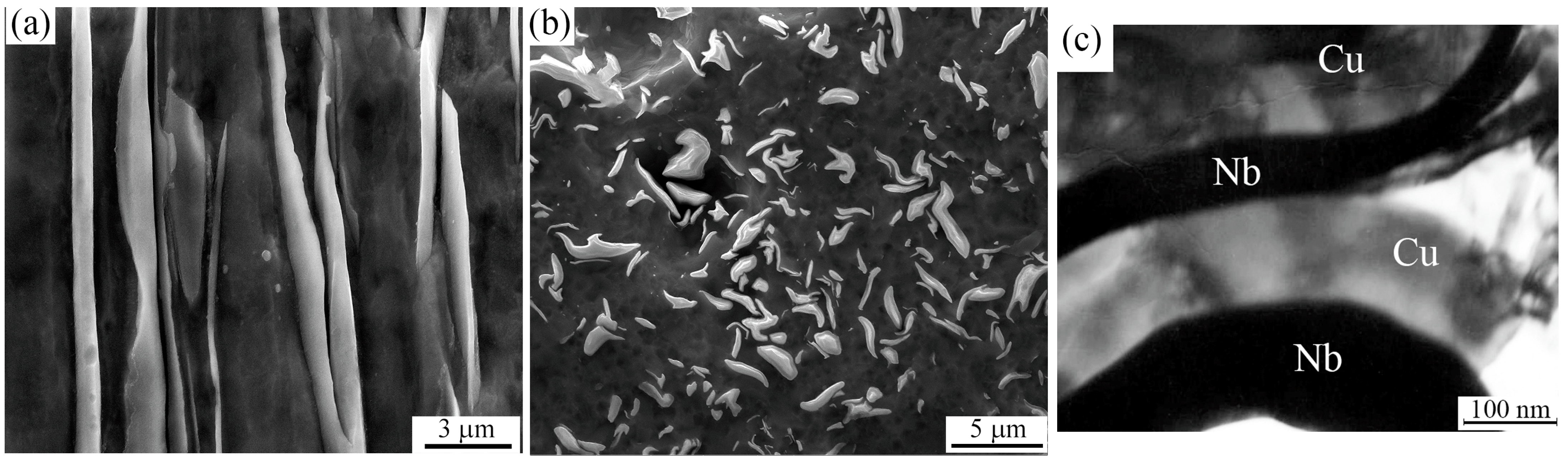
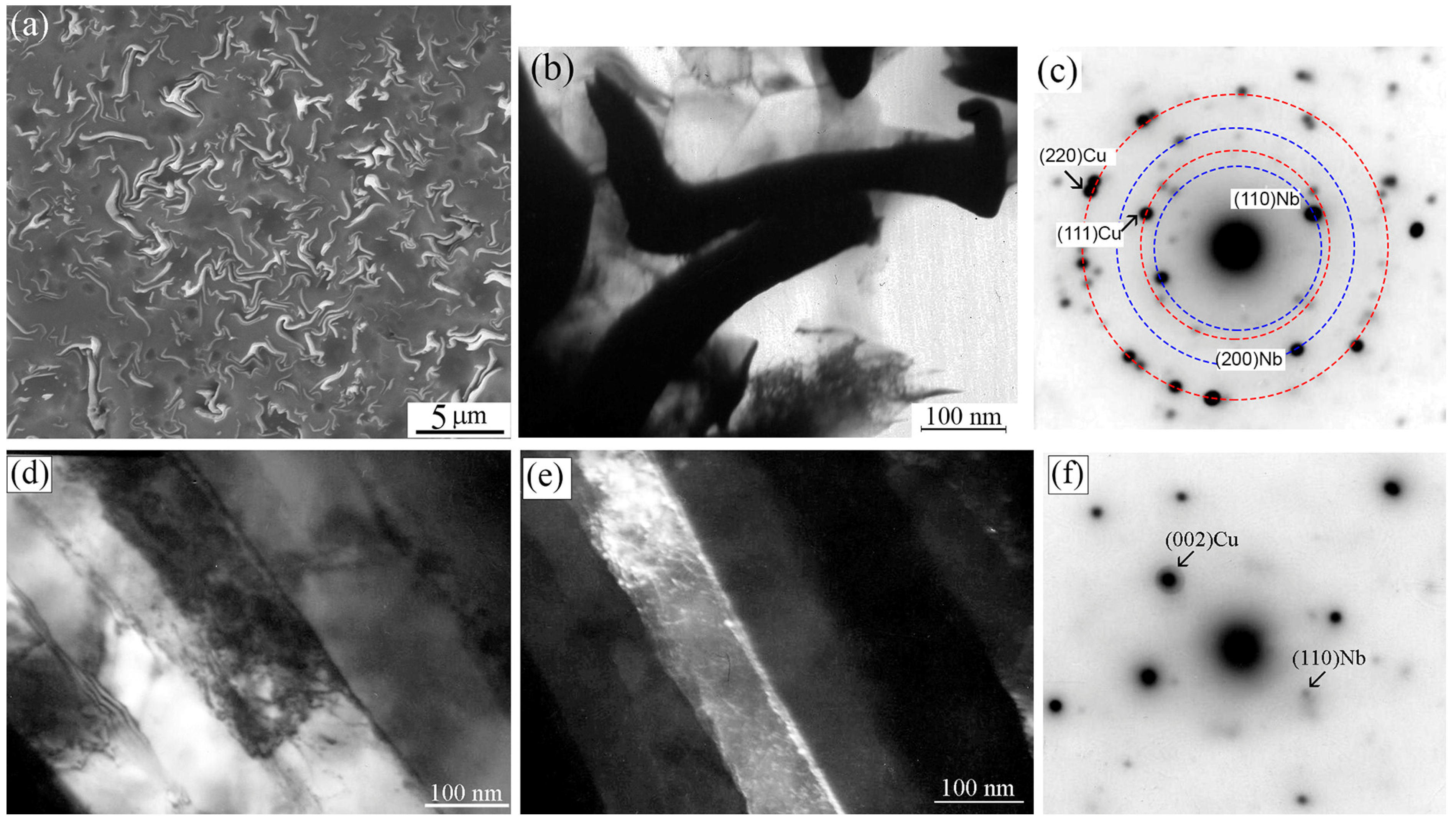
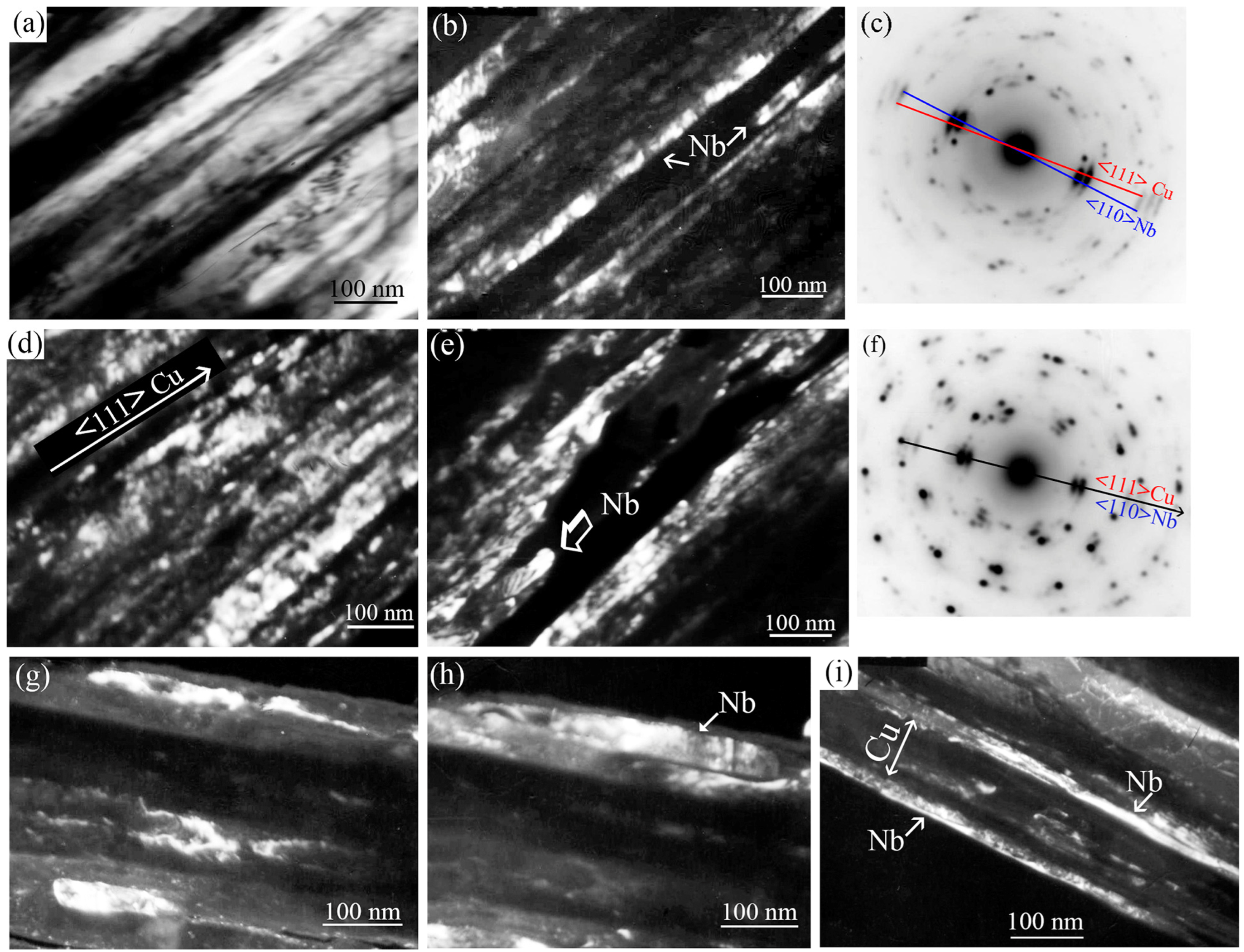
3.3. Structure of Cold Drawn Cu-7.7Nb Composite

3.3.1. Before Intermediate HT

In longitudinal sections of sample #1 (∅ 9.02 mm), niobium filaments are rows of light ribbons elongated along the wire drawing axis (Figure 5a). The cross-sections of sample #1 demonstrate extreme inhomogeneity in the shape and sizes of niobium filaments, most of which have an elongated shape without sharp bends and without twisting around copper grains (Figure 5b,c). Niobium filaments are heterogeneous in size, both in length (0.5 µm–3 µm) and thickness. For example, in the TEM image shown in Figure 5c, one niobium filament has a thickness of about 50 nm, and another is about 150 nm. In principle, the inhomogeneity of the niobium filament sizes is characteristic of in situ composites at early stages of deformation, in which both large dendrite “stems” and sections of thin “branches” were initially present in the dendritic structure of niobium. The TEM image in Figure 5c demonstrates that niobium filaments practically do not twist around copper grains and the copper grains have a low dislocation density and non-equiaxed shape with sizes of about 0.5–0.7 µm.
The main dimensional features of niobium filaments in the cross-sections of the samples calculated based on the SEM images are presented in Table 3. An average perimeter of niobium filaments is labeled as interface l. A ratio of the sum of interfaces of all filaments to the area of the analyzed SEM-image is labeled as the interface density La. In sample #1, the average thickness h of Nb filaments is 0.7 μm, interface l is 4.6 µm, the aspect ratio AsR is 7.4 and the interface density La is 0.6 μm/μm2 (Table 3).
The increase in true strain η from 3.21 (sample #1) to 5.03 (sample #2) leads to a decrease in the thickness of Nb filaments h from 0.7 µm to 0.17 μm, a twofold increase in aspect ratio and a threefold increase in interface density (Table 3). The Nb filaments in sample #2 become more curved (Figure 6a,b) with 2–3 smooth bends. As the TEM data in Figure 6b demonstrate, the niobium filaments in sample #2 are noticeably thinner than in sample #1 (see Figure 5c), with a pronounced ribbon shape and sharper bends. In addition, they are partly curved around copper grains. In electron diffraction patterns, alternating reflections of copper and niobium are located in the corresponding Debye rings (Figure 6c). The grains of copper matrix in the cross-sections of the wire are mostly equiaxed in shape with sizes of 0.2–0.4 μm. The dislocation density in copper grains is still low (Figure 6b), and some grains are practically free of dislocations, due to the dynamic recrystallization of copper under drawing [18,23]. Thus, the wire strengthening under drawing is caused by thinning of Nb filaments, increasing interface density and distortions of Nb lattice, rather than by Cu grain refinement.
TEM images of longitudinal sections of sample #2 demonstrate that elongated Nb filaments alternate with wider copper interlayers (Figure 6d,e). Not all boundaries between Nb and Cu are straight and sharp, as there are wavy and wide boundaries with a high density of dislocations (Figure 6d). The presence in some electron diffraction patterns of bright reflections from (002) crystallographic planes of copper (Figure 6f) is the consequence of double texture in cold-drawn copper discussed above in the X-ray data section. The dark-field TEM image from (002)Cu reflection (Figure 6e) demonstrates elongated copper grains oriented parallel to the additional <001> texture direction.
In sample #3 (η = 5.74), the density of Nb filaments in the copper matrix increases significantly (Table 3), and their shape becomes even more curved (Figure 7a). The average thickness of Nb filaments decreases to 0.07 μm, whereas the aspect ratio increases to 18.3. In the structure of this sample, there are separate thin long curved niobium filaments with a maximal aspect ratio of about 60 (AsR, max in Table 3). TEM images, one of which is shown in Figure 7b, demonstrate Nb filaments twisted around the copper grains. According to Ref. [18], the twisting of Nb filaments around copper grains is accompanied by the formation of semi-coherent interfaces between the grains of ribbon-like niobium filaments and copper matrix. Most of the electron diffraction patterns are the same as in the previous sample, with point reflections of Cu and Nb on the corresponding Debye rings. However, some electron diffraction patterns demonstrate a weak diffuse ring corresponding to the (110)Nb interplanar spacing (Figure 7c), which indicates the presence of small areas with an amorphous structure on Cu/Nb interfaces. Dark-field TEM images demonstrate elongated niobium filaments (Figure 7d) and copper matrix grains (Figure 7e) located in the directions <110>Nb ‖ DA and <111>Cu ‖ DA, respectively.
The misorientation angle between the <110>Nb and <111>Cu directions in the electron diffraction pattern shown in Figure 7 is approximately 5°, which indicates a semi-coherent character of Cu/Nb interfaces [19,21,41,42]. The interface density La increases from 1.7 µm/µm2 in sample #2 to 5.1 µm/µm2 in sample #3, and the latter value is approximately ten times higher than in sample #1 (Table 3). The threefold increase in the interface density did not cause a sharp increase in the strength of the composite (Table 1). Taking into account the sharp decrease in the relative elongation δ of sample #3 (Table 1), it can be assumed that at this step of drawing the strain hardening plays the main role, and compositional hardening has not formed completely.

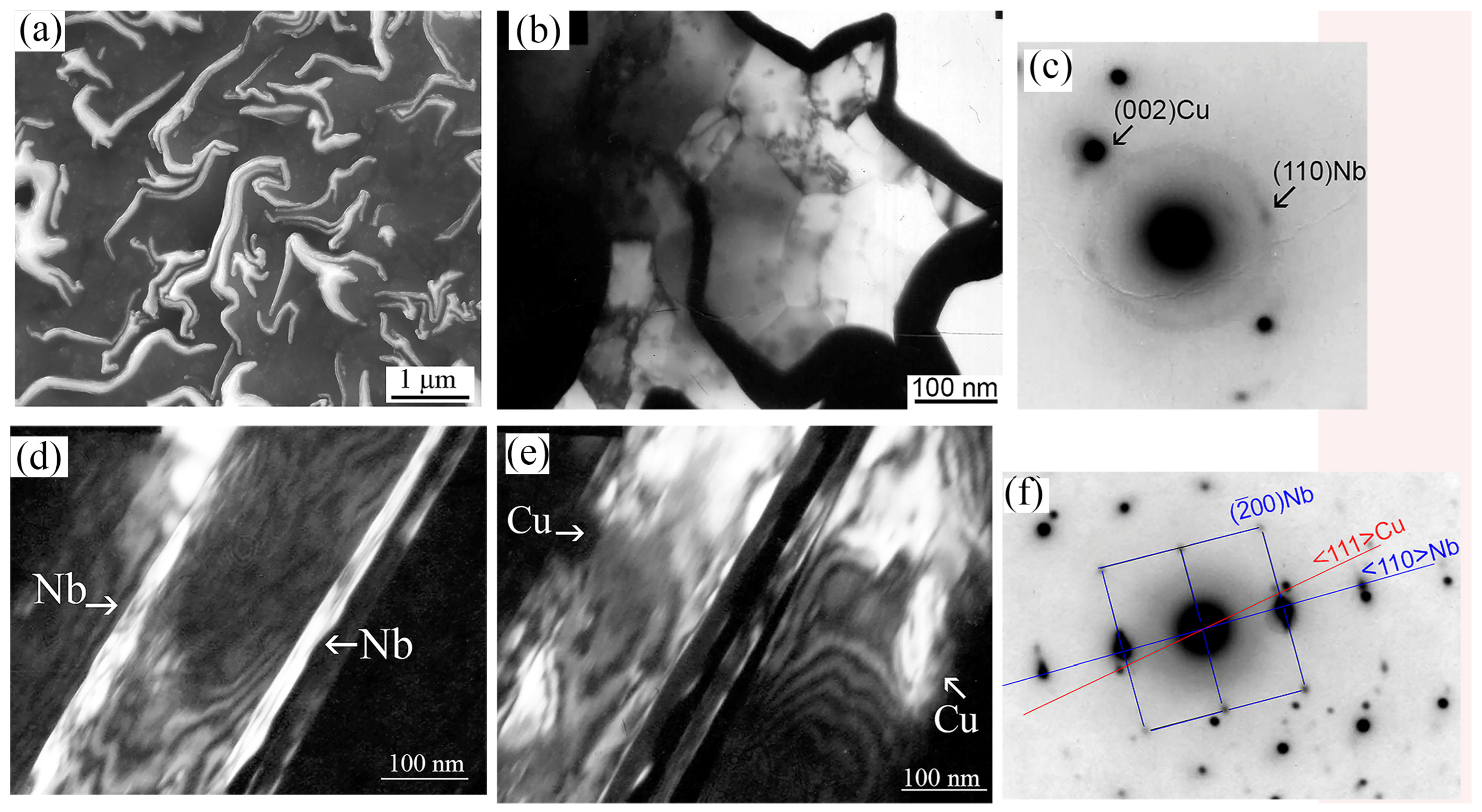
3.3.2. After Intermediate HT

According to SEM images, after HT at 550 °C (sample #4-0), Nb filaments thicken in cross sections, acquiring a more rounded “swollen” shape, and thin sections appear near the filament bends (Figure 8a). The average value of the aspect ratio of Nb filaments decreases sharply to 7.8 (Table 3). The changes in morphology of the niobium ribbons in cross-sections of the wire indicate the beginning of the coagulation processes in niobium which lead to the disruption of bonds between Nb filaments and the Cu matrix. As a result of the initial stages of coagulation, in longitudinal sections of sample #4, a sub-relief appears (Figure 8b) on the surface of the previously smooth Nb ribbons. This coagulation of Nb filaments is the main reason for the decrease in the strength of the sample under HT even at the lowest temperature (Table 1, sample #4-0).
Numerous TEM images of longitudinal sections of sample #4-0, one of which is shown in Figure 8c, demonstrate the appearance of thicker filaments and an increase in the variation in the filament thicknesses. The Nb/Cu interface becomes wave-like (with thickened and narrowed areas) (Figure 8c) rather than straight as in the sample before HT (Figure 7e). The dislocation density in niobium filaments decreases under HT, leading to the decrease in microstresses in niobium, according to the above X-ray data, and to a significant increase in the ductility of the composite wire, even after the annealing at the lowest of tested temperatures. However, the non-uniform distribution of brightness of contrast in the dark-field TEM image along the Nb filaments (Figure 8c) indicates heterogeneity of internal elastic stress distribution. Hence, after HT at 550 °C in some sections of Nb filaments, the internal stresses are retained.
After HT at 700 °C, Nb filaments continue to thicken in the cross sections (Figure 8d). In the longitudinal sections, some of the filaments acquire sausage-like (Figure 8e) and bamboo-like (Figure 8f) shapes with constrictions, and others disintegrate into fragments in the form of cylinders and discs (Figure 8e). TEM images in Figure 8e demonstrate that “bamboo-like” Nb filaments are practically free of dislocations. The Nb filaments aspect ratio decreases from 18.3 before HT to 4.6 after HT at 700 °C (Table 3, sample # 5-0).
With an increase in the annealing temperature to 800 °C, Nb filaments continue to “swell” (Figure 8g,h), losing their ribbon-like shape and splitting into fragments. The average thickness of Nb filaments increases from 70 nm before HT to 250 nm after HT at 800 °C. According to SEM (Figure 8g,h) and TEM (Figure 8i) images, a large number of single filaments of almost circular cross-sections (AsR~1) appear in the structure, i.e., individual fragments of niobium ribbons are spheroidized. One of these spheroidized filaments is seen in Figure 8i. As a result of the coagulation and the fragmentation of niobium ribbons under HT, the interface, aspect ratio and interface density of Nb filaments decrease (sample #6-0, Table 3).
According to TEM, with an increase in the HT temperature to 800 °C, the grains of both the copper matrix and the niobium filaments become almost free of dislocations, which only in small amounts remain at grain boundaries. These results allow us to conclude that the processes of coagulation and “swelling” in niobium filaments lead both to the relaxation of internal stresses in Nb filaments and the breakdown of the previously established bonds at Cu/Nb interfaces.
Note that similar morphological changes in the shape of niobium filaments were observed under the study of thermal stability in high-strength Cu-Nb MC wires with higher niobium content (16–20 wt.%) [19,24,40,42,43,44,45,46,47,48]. According to Ref. [43], morphological changes in two-phased composites result from the intensification of diffusion processes under HT, and with an increase in the annealing temperature, some niobium rods are spheroidized to reduce the surface energy.
Many authors [44,45,46,47] believe that the structure evolution of the ribbon-like niobium under annealing occurs only at the Cu/Nb interfaces. But some researchers [40,49] demonstrate that the change of the niobium ribbon morphology begins inside the filaments, because the internal energy stored in the niobium under deformation leads to the formation of low-angle boundaries, and the temperature-induced motion of these low-angle boundaries under HT leads to the nucleation of the grooves inside niobium filaments. As the temperature increases, the grooves gradually deepen, leading to splitting and then to the spheroidization of Nb filaments to minimize internal energy. Authors of Ref. [49] observed an internal friction peak (the so-called Snook peak [50]) in Cu-18Nb composite heat-treated at 550 °C and an abnormal decrease in Nb filaments microhardness to the value of microhardness of recrystallized niobium.
These results, in the opinion of the authors of Ref. [49], indicate that the change in the structure of niobium under HT occurs not only at Cu/Nb interfaces, but also inside niobium filaments. Note that despite the morphological changes in niobium filaments and sharp drop in the strength of the composite wire after all tested HT modes (samples # 4-0, # 5-0, # 6-0, Table 1), the further wire deformation to diameter of 0.27 mm leads to the increase in UTS to the values of about 1000 MPa for all heat-treated samples (samples #4-1, #5-1, and #6-1, Table 1).

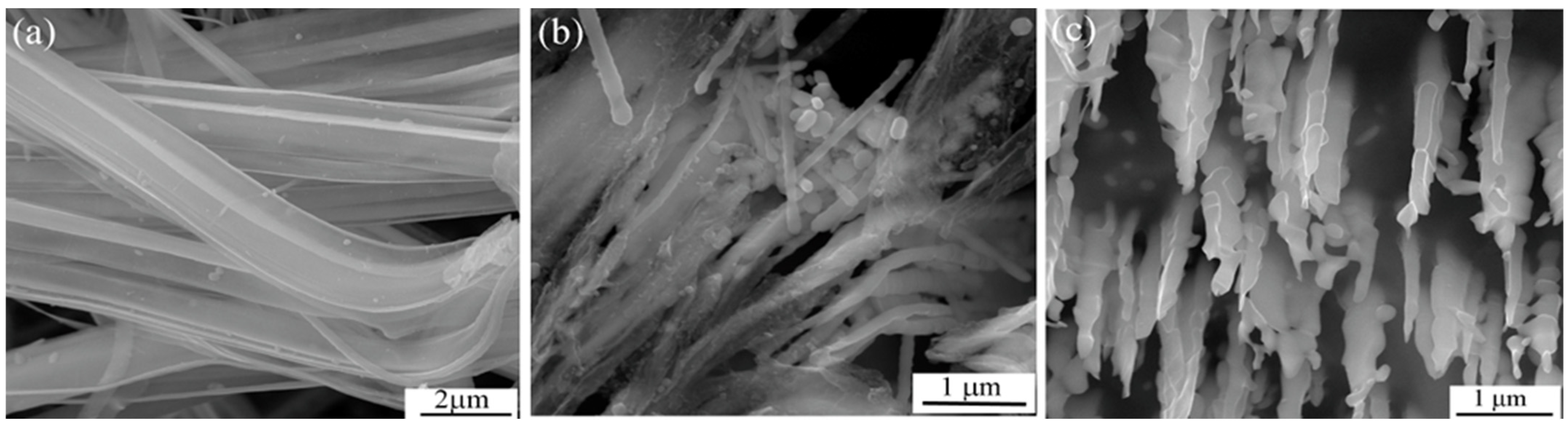
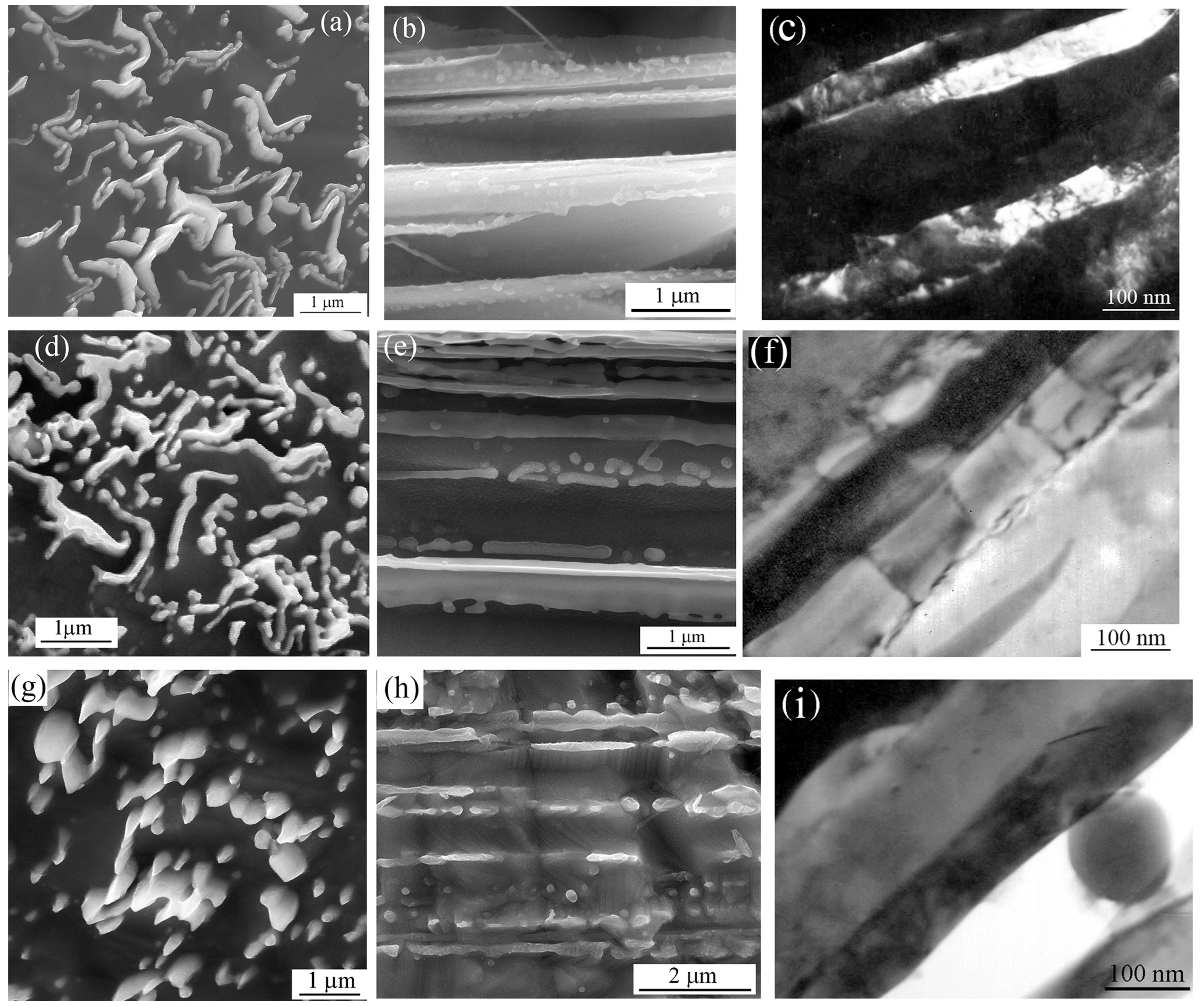
3.3.3. Cold Drawing of Heat-Treated Wires

TEM images of longitudinal sections of the wires cold-drawn after HT to the diameter of 0.27 mm (samples #4-1, #5-1 and #6-1) are presented in Figure 9. The structure of all heat treated at different temperatures samples consists of alternating layers of copper and niobium with clear straight boundaries parallel to the drawing axis. The thickness of Nb filaments is about 25–30 nm for the samples drawn after HTs at 550 °C (Figure 9a,b) and 700 °C (Figure 9e), and 35–40 nm after HT at 800 °C (Figure 9g,h). The copper interlayer thicknesses are about 70 nm in sample #4-1 (Figure 9a,b), 80 nm in sample #5-1 (Figure 9d) and 95 nm in sample #6-1 (Figure 9i). The dislocation density in many areas of the copper matrix of these samples is low. One such TEM image of copper layers, practically free of dislocations, is shown in Figure 9a.
However, despite the similarity of the structure of these three samples, the TEM method also reveals some differences in their fine structure. Thus, in sample #4-1, the size distribution of niobium filaments and contrast in dark-field TEM images of the niobium filaments are uniform (Figure 9b). This indicates the uniform deformability of niobium filaments and the uniform distribution of internal stresses in them. This confirms the conclusion made in Ref. [49], according to which the softening of the copper matrix even under a short intermediate annealing creates more favorable conditions for further uniform deformation of niobium filaments.
In many-electron diffraction patterns from this sample, the angle between the <110>Nb and <111>Cu directions is about 4–5 degrees (Figure 9c), which is a sign of a semi-coherent boundary at the Cu/Nb interface. As previously mentioned, this type of electron diffraction pattern was observed for sample #3 before HT (Figure 7g) and was not observed in the heat-treated samples. That is, the semi-coherent bond at the Cu/Nb interface, broken by HT, is restored after drawing the heat-treated wires to a diameter of 0.27 mm. Note that in TEM-images of sample #4-1 longitudinal sections, there are no breaks of niobium filaments (for example, see Figure 9b), which again confirms the good deformability of the wire after this HT mode.
In sample #5-1, drawn after HT at a higher temperature of 700 °C, areas with partially broken Nb filaments appear (shown with white arrows in Figure 9e). In some electron diffraction patterns of this sample, <110>Nb and <111>Cu directions do not diverge by an angle of 4–5 degrees, but completely coincide (Figure 9f). Hence, the coherence of the Cu/Nb interface boundaries is manifested to a lesser extent in this sample.
TEM images of sample #6-1, drawn after HT at 800 °C, demonstrate that niobium filaments have an uneven, discontinuous, and more rounded shape (Figure 9g–i). The thickness of niobium filaments and copper interlayers in this sample is larger than in sample #4-1. The number of structural sections whose electron diffraction patterns would indicate the presence of coherence at the Cu/Nb interfaces is small.
Thus, based on the results of TEM studies, one can conclude that the annealing temperature of intermediate HT, although insignificantly, still affects the structure of samples drawn after HT. The sample drawn after HT at the lowest of tested temperatures 550 °C has an optimal structure with thin Nb filaments parallel to the drawing axes and semi-coherent boundaries on the Cu/Nb interface. But the internal stresses in the niobium filaments of this sample, as noted above, are higher than in the samples heat treated at higher temperatures.
Figure 10 shows the dependences of UTS and relative elongation δ on the true strain of Cu-7.7Nb wire before and after HT at 700 °C, 1h. Figure 10a clearly demonstrates that the HT leads to an almost twofold decrease in the strength of the wire.
On the other hand, the ductility of the wire is increased by a factor of ten (Figure 10b), which makes it possible to draw the wire to the diameter of 0.05 mm (η = 13.6) and reach the tensile strength of 1236 MPa (sample #5-2, Table 1). Similar dependences of UTS and δ on strain η were observed for the samples of the MC wires with two other tested HT modes. The samples of composite wires after all tested HT temperatures were successfully cold drawn to the diameter of 0.05 mm (Table 1).
Thus, the choice of annealing temperature should be determined by a trade-off between the minimum possible destruction of the structure of ribbon-like niobium filaments and the copper–niobium interfaces under HT and the maximum reduction of internal stresses in the niobium.

4. Summary

The evolution of the structure of in situ Cu-7.7Nb microcomposite (MC) wires under cold drawing and intermediate heat treatment (HT) has been studied by SEM, TEM and X-ray analysis.
Intermediate HT at 500, 700 and 800 °C leads to an increase in the ductility of the Cu-7.7Nb wire which, according to the X-ray data, is due to the removal of internal microstresses in the Nb filaments.
According to SEM and TEM data, the removal of internal microstresses in Nb filaments under the HT results from significant changes in their morphology accompanied by an increase in their thickness and a decrease in the aspect ratio, interface and interface density. These changes are more pronounced, the higher the HT temperatures.
The HTs lead to the destruction of semi-coherent bonds on Cu/Nb interfaces. Further deformation of the heat-treated wires to the diameter of 0.27 mm leads to a restoration of Nb filament morphology and semi-coherent boundaries on Cu/Nb interfaces, which results in a sharp increase in UTS to values higher than 1000 MPa.
The stability of the <110>Nb texture to HT plays a positive role in the restoration of the semi-coherent character of the Cu/Nb interfaces under the subsequent drawing.
Thus, the choice of the intermediate annealing temperature should be determined by a trade-off between the minimum possible destruction of the ribbon shape of Nb filaments at Cu/Nb interfaces and the maximum reduction in internal stresses in Nb. In the present study, this optimal compromise is provided by the annealing mode of 700 °C, 1 h, resulting in the highest UTS (1236 MPa) at the final diameter of 0.05 mm.
The decrease in the concentration of Nb to 7.7% compared to the previously used 16–20% and the application of intermediate heat treatments make it possible to obtain ultrathin high-strength wires of extremely small diameter under the true strain of 13.6, which is not achievable in MCs with higher Nb concentration.
The results obtained in this study make it possible to optimize the process of obtaining high-strength wires, taking into account possible forecasts of changes in structural characteristics under the influence of various production factors such as the degree of deformation, duration and temperature of annealing, and to predict the thermal stability of the wire under its operation. According to the study presented by the developers of these wires [6], the tensile strength achieved immediately after the production of the wire may subsequently decrease only slightly during the first two to three months of holding at room temperature. However, this decrease does not exceed 5% of the initial value, and in the future, the strength characteristics of the wire will not change.

Author Contributions

Conceptualization, methodology and investigation, I.L.D. and E.N.P.; SEM studies, E.I.P.; writing and original draft preparation, I.L.D., E.N.P. and E.I.P.; review and editing, I.L.D. and E.N.P. All authors have read and agreed to the published version of the manuscript.

Funding

This research was carried out within the state assignment of the Ministry of Science and Higher Education of the Russian Federation (themes “Pressure”, No 122021000032-5 and “Spin”, No 122021000036-3).

Data Availability Statement

The data presented in this study are available on request from the corresponding author.

Acknowledgments

The authors express their sincere gratitude to the Head of the scientific technical division of RC “Nanoelectro”, Natalia E. Khlebova, and the Director of RC “Nanoelectro”, Vitaly I. Pantsyrny, under whose leadership the wires under study were worked out, deformed, heat-treated and their mechanical properties measured. The authors are especially thankful to N.E. Khlebova for her interesting ideas and fruitful discussion of the research. The authors are grateful to Boris D. Antonov for the help in XRD analysis, to Leonid N. Lobanov for assistance in the statistical analysis of the niobium filaments dimension characteristics, and to Vitaly E. Patrakov for assistance in preparing the text according to the MDPI template. The SEM, TEM and partly X-ray studies were carried out using the equipment of the Collaborative Access Center, “Testing Center of Nanotechnology and Advanced Materials, of the IMP UB RAS.

Conflicts of Interest

The authors declare no conflict of interest.

References

  1. Zhu, W.; Yang, C.; Yu, Z.; Xiao, J.; Xu, Y. Impact of Defects in Steel-Concrete Interface on the Corrosion-Induced Cracking Propagation of the Reinforced Concrete. KSCE J. Civ. Eng. 2023, 27, 2621–2628. [Google Scholar] [CrossRef]
  2. Zhu, W.; Yu, Z.; Yang, C.; Dong, F.; Ren, Z.; Zhang, K. Spatial distribution of corrosion products influenced by the initial defects and corrosion-induced cracking of the concrete. J. Test. Eval. 2023, 154, 16. [Google Scholar] [CrossRef]
  3. Levin, Z.S.; Demkowicz, M.J.; Hartwig, K.T. Copper-Tantalum Metal Matrix Composites Consolidated from Powder Blends by Severe Plastic Deformation. Metals 2021, 11, 1010. [Google Scholar] [CrossRef]
  4. Eze, A.A.; Sadiku, E.R.; Kupolati, W.K.; Ndambuki, J.M.; Snyman, J.; Ibrahim, I.D. Spark Plasma Sintering of Copper-Niobium-Graphite Composites, and the Investigations of Their Microstructure and Properties. Metals 2022, 12, 574. [Google Scholar] [CrossRef]
  5. Tian, X.; Zhao, Y.; Gu, T.; Guo, Y.; Xu, F.; Hou, H. Cooperative effect of strength and ductility processed by thermomechanical treatment for Cu–Al–Ni alloy. Mater. Sci. Eng. A 2022, 849, 143485. [Google Scholar] [CrossRef]
  6. Fang, J.X.; Wang, J.X.; Wang, Y.J.; He, H.T.; Zhang, D.B.; Cao, Y. Microstructure evolution and deformation behavior during stretching of a compositionally inhomogeneous TWIP-TRIP cantor-like alloy by laser powder deposition. Mater. Sci. Eng. A 2022, 847, 143319. [Google Scholar] [CrossRef]
  7. Zhang, Z.; Chen, J.; Wang, J.; Han, Y.; Yu, Z.; Wang, Q.; Zhang, P.; Yang, S. Effects of solder thickness on interface behavior and nanoindentation characteristics in Cu/Sn/Cu microbumps. Weld. World 2022, 66, 973–983. [Google Scholar] [CrossRef]
  8. Pantsyrnyi, V.I. Status and perspectives for microcomposite winding materials for high field pulsed magnets. IEEE Trans. Appl. Supercond. 2002, 12, 1189–1194. [Google Scholar] [CrossRef]
  9. Dubois, J.B.; Thilly, L.; Renault, P.O.; Lecouturier, F. Cu–Nb Nanocomposite Wires Processed by Severe Plastic Deformation: Effects of the Multi-Scale Microstructure and Internal Stresses on Elastic-Plastic Properties. Adv. Eng. Mater. 2012, 14, 998–1003. [Google Scholar] [CrossRef]
  10. Spencer, K.; Lecouturier, F.; Thilly, L.; Embury, J.D. Established and emerging materials for use as high-field magnet conductors. Adv. Eng. Mater. 2004, 6, 290–297. [Google Scholar] [CrossRef]
  11. Shikov, A.; Pantsyrnyi, V.; Vorobieva, A.; Khlebova, N.; Silaev, A. High strength, high conductivity Cu–Nb based conductors with nanoscaled microstructure. Phys. C Supercond. 2001, 354, 410–414. [Google Scholar] [CrossRef]
  12. Shikov, A.K.; Pantsyrnyi, V.I.; Vorob’eva, A.E.; Sud’ev, S.V.; Khlebova, N.E.; Silaev, A.K.; Belyakov, N.A. Copper-niobium high-strength and high-conductivity winding wires for pulsed magnets. Met. Sci. Heat Treat. 2002, 44, 491–495. [Google Scholar] [CrossRef]
  13. Swenson, C.A.; Marshall, W.S.; Miller, E.L.; Pickard, K.W.; Gavrilin, A.V.; Han, K.; Schneider-Muntau, H.J. Pulse magnet development program at NHMFL. IEEE Trans. Appl. Supercond. 2004, 14, 1233–1236. [Google Scholar] [CrossRef]
  14. Pantsyrnyi, V.; Shikov, A.; Vorobieva, A.; Soudiev, S.; Sergeev, V.; Dergunova, E.; Sinitsyn, I.; Beliakov, N.; Kukin, S. Nb3Sn superconducting wire, reinforced by Cu-Nb microcomposite material. IEEE Trans. Appl. Supercond. 2004, 14, 996–999. [Google Scholar] [CrossRef]
  15. Pantsyrny, V.; Shikov, A.; Vorobieva, A. Nb3Sn material development in Russia. Cryogenics 2008, 48, 354–370. [Google Scholar] [CrossRef]
  16. Pantsyrny, V.I.; Shikov, A.K.; Vorobieva, A.E.; Khlebova, N.E.; Kozlenkova, N.I.; Drobishev, V.A.; Potapenko, I.I.; Beliakov, N.A.; Polikarpova, M.V. High strength, high conductivity microcomposite Cu-Nb wires with cross sections in the range of 0.01–100 mm2. IEEE Trans. Appl. Supercond. 2008, 18, 616–619. [Google Scholar] [CrossRef]
  17. Deng, L.; Yang, X.; Han, K.; Lu, Y.; Liang, M.; Liu, Q. Microstructure and texture evolution of Cu–Nb composite wires. Mater. Charact. 2013, 81, 124–133. [Google Scholar] [CrossRef]
  18. Deng, L.; Han, K.; Hartwig, K.T.; Siegrist, T.M.; Dong, L.; Sun, Z.; Yang, X.; Liu, Q. Hardness, electrical resistivity, and modeling of in situ Cu–Nb microcomposites. J. Alloys Compd. 2014, 602, 331–338. [Google Scholar] [CrossRef]
  19. Deryagina, I.L.; Popova, E.N.; Valova-Zaharevskaya, E.G.; Patrakov, E.I. Structure and thermal stability of high-strength Cu–18Nb composite depending on the degree of deformation. Phys. Met. Metallogr. 2018, 119, 92–102. [Google Scholar] [CrossRef]
  20. Deng, L.; Liu, Z.; Wang, B.; Han, K.; Xiang, H. Effects of interface area density and solid solution on the microhardness of Cu-Nb microcomposite wires. Mater. Charact. 2019, 150, 62–66. [Google Scholar] [CrossRef]
  21. Snoeck, E.; Lecouturier, F.; Thilly, L.; Casanove, M.J.; Rakoto, H.; Coffe, G.; Askenazy, S.; Peyrade, J.P.; Roucau, C.; Pantsyrny, V.; et al. Microstructural studies of in situ produced filamentary Cu/Nb wires. Scr. Mater. 1998, 38, 1643–1648. [Google Scholar] [CrossRef]
  22. Sauvage, X.; Renaud, L.; Deconihout, B.; Blavette, D.; Ping, D.H.; Hono, K. Solid state amorphization in cold drawn Cu/Nb wires. Acta Mater. 2001, 49, 389–394. [Google Scholar] [CrossRef]
  23. Leprince-Wang, Y.; Han, K.; Huang, Y.; Yu-Zhang, K. Microstructure in Cu–Nb microcomposites. Mater. Sci. Eng. A 2003, 351, 214–223. [Google Scholar] [CrossRef]
  24. Pantsyrny, V.; Shikov, A.; Vorobieva, A.; Khlebova, N.; Kozlenkova, N.; Potapenko, I.; Polikarpova, M. Stability aspects of the high strength high conductivity microcomposite Cu-Nb wires properties. IEEE Trans. Appl. Supercond. 2006, 16, 1656–1659. [Google Scholar] [CrossRef]
  25. Permyakova, I.; Glezer, A. Amorphous-Nanocrystalline Composites Prepared by High-Pressure Torsion. Metals 2020, 10, 511. [Google Scholar] [CrossRef]
  26. Wang, J.; Zhao, F.; Liu, X. Nb Phase Position Marking for Clarifying the Formation Process of Cu-Al Composite Interfacial Phases in Continuous Composite Casting. Metals 2023, 13, 1045. [Google Scholar] [CrossRef]
  27. Straumal, B.B.; Mazilkin, A.A.; Baretzky, B. Grain boundary complexions and pseudopartial wetting. Curr. Opin. Solid State Mater. Sci. 2016, 20, 247–256. [Google Scholar] [CrossRef]
  28. Straumal, B.B.; Kogtenkova, O.A.; Straumal, A.B.; Baretzky, B. Grain boundary wetting-related phase transformations in Al and Cu-based alloys. Rev. Lett. Mater. 2018, 8, 364–371. [Google Scholar] [CrossRef]
  29. Chinh, N.Q.; Valiev, R.Z.; Sauvage, X.; Varga, G.; Havancsak, K.; Kawasaki, M.; Straumal, B.B.; Langdon, T.G. Grain Boundary Phenomena in an Ultrafine-Grained Al–Zn Alloy with Improved Mechanical Behavior for Micro-Devices. Adv. Eng. Mater. 2014, 16, 1000–1009. [Google Scholar] [CrossRef]
  30. Popova, E.N.; Popov, V.V. Dislocation and grain structure formation in Nb filaments of different geometry at fabrication of Nb3Sn-based superconducting wires. Mater. Char. 2020, 167, 110488–110495. [Google Scholar] [CrossRef]
  31. Munitz, A.; Bamberger, M.; Venkert, A.; Landau, P.; Abbaschian, R. Phase selection in supercooled Cu–Nb alloys. J. Mater. Sci. 2009, 44, 64–73. [Google Scholar] [CrossRef]
  32. Ekiz, E.H.; Lach, T.G.; Averback, R.S.; Mara, N.A.; Beyerlein, I.J.; Pouryazdan, M.; Hahn, H.; Bellon, P. Microstructural evolution of nanolayered Cu–Nb composites subjected to high-pressure torsion. Acta Mater. 2014, 72, 178–191. [Google Scholar] [CrossRef]
  33. Popova, E.N.; Deryagina, I.L. Evolution of Structure of Cu–Nb Composite under High-Pressure Torsion and Subsequent Annealing. Phys. Met. Metallogr. 2020, 121, 1182–1187. [Google Scholar] [CrossRef]
  34. Quelennec, X.; Menand, A.; Le Breton, J.M.; Pippan, R.; Sauvage, X. Homogeneous Cu–Fe supersaturated solid solutions prepared by severe plastic deformation. Phil. Mag. 2010, 90, 1179–1195. [Google Scholar] [CrossRef]
  35. Pantsyrny, V.; Polikarpova, M.; Lukyanov, P.; Guryev, V.; Khlebova, N.E.; Sergeev, V. The study of strengthening and the electrical resistivity of deformation processed Cu/Cu-16% Nb and Cu/Cu-7.7% Nb microcomposites. IEEE Trans. Appl. Supercond. 2020, 30, 1–4. [Google Scholar] [CrossRef]
  36. Kozlenkova, N.I.; Pantsyrnyi, V.I.; Nikulin, A.D.; Shikov, A.K.; Potapenko, I.I. Electrical conductivity of high-strength Cu-Nb microcomposites. IEEE Trans. Magnet. 1996, 32, 2921–2924. [Google Scholar] [CrossRef]
  37. Volkov, A.Y.; Antonov, B.D.; Patrakov, E.I.; Volkova, E.G.; Komkova, D.A.; Kalonov, A.A.; Glukhov, A.V. Abnormally high strength and low electrical resistivity of the deformed Cu/Mg-composite with a big number of Mg-filaments. Mater. Des. 2020, 185, 108276. [Google Scholar] [CrossRef]
  38. Demakov, S.L.; Loginov, Y.N.; Illarionov, A.G.; Ivanova, M.A.; Karabanalov, M.S. Effect of annealing temperature on the texture of copper wire. Phys. Met. Metallogr. 2012, 113, 681–686. [Google Scholar] [CrossRef]
  39. Raabe, D.; Heringhaus, F.; Hangen, U.; Gottstein, G. Investigation of a Cu-20 mass% Nb in situ composite, part I: Fabrication, microstructure and mechanical properties. Z. Met. 1995, 86, 405–415. [Google Scholar] [CrossRef]
  40. Deng, L.; Wang, B.; Han, K.; Niu, R.; Xiang, H.; Hartwig, K.T.; Yang, X. Response of microstructure to annealing in in situ Cu–Nb microcomposite. J. Mater. Sci. 2019, 54, 840–850. [Google Scholar] [CrossRef]
  41. Dupouy, F.; Snoeck, E.; Casanove, M.J.; Roucau, C.; Peyrade, J.P.; Askenazy, S. Microstructural characterization of high strength and high conductivity nanocomposite wires. Scr. Mater. 1996, 34, 1067–1073. [Google Scholar] [CrossRef]
  42. Popova, E.N.; Deryagina, I.L.; Valova-Zaharevskaya, E.G.; Ruello, M.L.; Popov, V.V., Jr. Microstructural Features in Multicore Cu–Nb Composites. Materials 2021, 14, 7033. [Google Scholar] [CrossRef] [PubMed]
  43. Hong, S.I.; Hill, M.A. Microstructural stability of Cu–Nb microcomposite wires fabricated by the bundling and drawing process. Mater. Sci. Eng. A 2000, 281, 189–197. [Google Scholar] [CrossRef]
  44. Wan, H.; Shen, Y.; Wang, J.; Shen, Z.; Jin, X. A predictive model for microstructure evolution in metallic multilayers with immiscible constituents. Acta Mater. 2012, 60, 6869–6881. [Google Scholar] [CrossRef]
  45. Zheng, S.J.; Wang, J.; Carpenter, J.S.; Mook, W.M.; Dickerson, P.O.; Mara, N.A.; Beyerlein, I.J. Plastic instability mechanisms in bimetallic nanolayered composites. Acta Mater. 2014, 79, 282–291. [Google Scholar] [CrossRef]
  46. Misra, A.; Hoagland, R.G.; Kung, H. Thermal stability of self-supported nanolayered Cu/Nb films. Phil. Mag. 2004, 84, 1021–1028. [Google Scholar] [CrossRef]
  47. Thilly, L.; Lecouturier, F.; Von Stebut, J. Size-induced enhanced mechanical properties of nanocomposite copper/niobium wires: Nanoindentation study. Acta Mater. 2002, 50, 5049–5065. [Google Scholar] [CrossRef]
  48. Lei, R.; Wang, M.; Xu, S.; Wang, H.; Guangrun, C. Microstructure, Hardness Evolution, and Thermal Stability Mechanism of Mechanical Alloyed Cu-Nb Alloy during Heat Treatment. Metals 2016, 6, 194. [Google Scholar] [CrossRef]
  49. Khlebova, N.E. Research of Structure Formation and Stress State in Composites upon the Fabrication of Nb3Sn-Based Superconductors. Ph.D. Thesis, A.A. Bochvar Institute of Inorganic Materials, Moscow, Russia, 1997. Available online: https://search.rsl.ru/ru/record/01000233428 (accessed on 1 March 2000).
  50. Dahlstrom, N.; Dollins, C.C.; Wert, C. The cold-work peak in undeformed niobium. Acta Metal. 1971, 19, 955–963. [Google Scholar] [CrossRef]
Figure 1. SEM image of Cu-7.7Nb composite cross-section highlighted by the program for image analyses: (a) perimeters (interfaces) of niobium filaments; (b) areas of niobium filaments.
Metals 13 01576 g001
Figure 2. X-ray diffraction patterns of transverse (a,c) and longitudinal (b) sections of samples: (a,b) #1; (c) #3 (without HT), #4-0 (HT at 550 °C,1 h), #5-0 (HT at 700 °C,1 h), #6-0 (HT at 800 °C, 1 h).
Metals 13 01576 g002
Figure 3. Microstresses μ (%) in Nb filaments (■) and Cu matrix () of Cu-7.7Nb composite before HT (samples #1, #2, #3) and after HT (samples #4-0, #5-0, #6-0).
Metals 13 01576 g003
Figure 4. SEM images of Nb filaments etched out of copper matrix of Cu-Nb wire with diameter of 2.54 mm: (a) before HT (sample #3), (b) after HT at 700 °C, 1 h (sample #5-0), (c) after HT at 800 °C, 1 h (sample #6-0).
Metals 13 01576 g004
Figure 5. SEM (a,b) and TEM (c) images of longitudinal (a) and transverse (b,c) sections of sample #1 (Ø—9.02 mm, η = 3.21).
Metals 13 01576 g005
Figure 6. SEM (a) and TEM (bf) images of transverse (a,b) and longitudinal (d,e) sections of sample # 2 (Ø—3.63 mm, η—5.03): (b) bright-field TEM image; (c) corresponding selected area electron diffraction pattern (SAED); (d) bright-field TEM image; (e) dark-field image in (002)Cu reflection; (f) corresponding SAED, zone axis ~ [111]Nb.
Metals 13 01576 g006
Figure 7. SEM (a) and TEM (b,d,e) images of transverse (ac) and longitudinal (d,e) sections of sample #3 (Ø—2.54 mm); (b) bright-field TEM image; (c) corresponding selected area electron diffraction pattern (SAED); (d) dark-field TEM image in ( 1 ¯ 1 0)Nb reflection; (e) dark-field TEM image in (111)Cu reflection; (f) corresponding SAED with indicated directions <110> Nb and <111>Cu, zone axis [001]Nb.
Metals 13 01576 g007
Figure 8. SEM (a,b,d,e,g,h) and TEM (c,f,i) images of transverse (a,d,g) and longitudinal (b,c,e,f,h,i) sections of the samples with diameter of 2.5 mm (η = 5.74) after HT: 550 °C, 1 h, sample #4-0 (ac); 700 °C, 1 h, sample #5-0 (df); and 800 °C, 1 h, sample #6-0 (gi); (c) dark-field TEM image in (110)Nb reflection; (f,i) bright-field TEM images.
Metals 13 01576 g008
Figure 9. TEM images of longitudinal sections of Cu-7.7Nb wires cold drawn after intermediate HT to diameter of 0.27 mm. Samples: #4-1 (drawn after HT at 550 °C, 1 h) (ac), #5-1 (drawn after HT at 700 °C, 1 h) (df) and #6-1 (drawn after HT at 800 °C, 1 h) (gi); (a) bright field image; (b,e,g,h,i) dark field images in reflection (110)Nb with backlighting from (111)Cu; (d) dark field images in reflection (111)Cu; (c,f) SAEDs.
Metals 13 01576 g009
Figure 10. Ultimate tensile strength UTS (a) and relative elongation δ (b) versus true strain η of the Cu-7.7Nb wire drawn before (black symbols in the interval of strains 3.2 ≤ η ≤ 5.74) and after (color symbols in the interval of strains 5.74 ≤ η ≤ 13.6) HT at 700 °C, 1 h.
Metals 13 01576 g010
Table 1. Characteristics of the samples of Cu-7.7Nb wires.
SampleDiameter, mmH 1UTS, 2
MPa
δ, 3
%
Cold drawing before HT
#19.023.214707.0
#23.635.035604.0
#32.545.745743.0
HT at 550 °C/1 h
#4-02.545.7438027.0
Cold drawing after HT 550 °C/1 h
#4-10.2710.2110731.4
#4-20.0513.611950.7
HT at 700 °C/1 h
#5-02.545.7433928.0
Cold drawing after HT 700 °C/1 h
#5-10.2710.2110492.6
#5-20.0513.612360.95
HT at 800 °C/1 h
#6-02.545.7430629.0
Cold drawing after HT 800 °C/1 h
#6-10.2710.219803.5
#6-20.0513.612271.0
1 η—true strain; 2 UTS—ultimate tensile strength; 3 δ—relative elongation.
Table 2. Characteristics of the samples before and after HT according to the XRD data.
SampleηHTNbCu
I* (110), %µ, %I* (111), %I* (200), %µ, %Δ, %
#13.211000.3972150.1310.7
#25.031000.4573140.1210.7
#35.741000.5874140.1210.6
#4-05.74550 °C, 1 h1000.5374150.0710.5
#5-05.74700 °C, 1 h1000.4965170.0810.6
#6-05.74800 °C, 1 h1000.4563230.0810.7
I* is relative intensity of (hkl) X-ray peak relative to integrated intensity of all peaks of the phase in the XRD pattern (30 ≤ 2Θ ≤ 140); µ is microstress; Δ is parameter of mismatch for the (110)Nb and (111)Cu crystallographic planes.
Table 3. Dimensional characteristics of Nb filaments vs. deformation step and HT mode.
SampleØ
(mm)
ηHTl 1
(μm)
AsR 2h 3
(nm)
La 4 (μm/μm2)
avMinMaxavMaxav
#19.023.214.61.614.17.4220.700.6
#23.635.034.61.413.213.9350.171.7
#32.55.743.21.413.918.3590.075.1
#4-02.55.74550 °C, 1 h2.10.2310.07.0270.084.4
#5-02.55.74700 °C, 1 h1.30.1811.04.6260.163.5
#6-02.55.74800 °C, 1 h1.30.1713.03.0180.262.7
1 l is the Cu/Nb interface; 2 AsR is the aspect ratio of Nb filaments; 3 h is the Nb filaments thickness; 4 La is the interface density.
Disclaimer/Publisher’s Note: The statements, opinions and data contained in all publications are solely those of the individual author(s) and contributor(s) and not of MDPI and/or the editor(s). MDPI and/or the editor(s) disclaim responsibility for any injury to people or property resulting from any ideas, methods, instructions or products referred to in the content.

