1. Introduction
The unique properties of thin (~100 nm) metal films differ from bulk properties of the metals used for their production, and enable designing electronic devices with improved static and high-frequency performance, and developing brand new electronic devices. Lack of information on thin metal film properties dependency in local approximation on lateral (in the substrate plane–further (x,y) plane) dimensions of the film makes it practically impossible to simulate devices at micro- and nanoscale and use them with specified device characteristics.
The main mechanical and electrical properties of thin metal films and systems based on them are generally determined by their morphology, i.e., an aggregated characteristic involving the geometry of surfaces and interfaces as well as the substructure of metal layers and their solid solutions defined by dimensions, shape, and relative position of its components: grains, dendrites (crystallites) and dielectric interspaces between them. With this consideration in mind, we understand by the term ‘thin metal system geometry’ not only an external shape of the perimeter P limiting it in (x,y) plane, but also geometry of surfaces and interfaces forming the system, and its substructure defined by fractal structure of its components and their relative positions.
In most cases, metal films of nanometric thickness are basically a complex of conductive nanograins and crystallites located in one plane and separated from each other by dielectric interspaces (the Mayadas-Shatzkes model) [
1]. The growth of such films comes from expansion and intergrowth of germinative grains and crystallites, accompanied with increase of their thickness and conductivity [
2,
3,
4,
5,
6]. The phenomenon flowing or not flowing current through such systems, which are complex conductive and non-conductive local areas interleaving on the (
x,y) plane, is called percolation and is described by percolation theory [
7]. In most works on this subject, electromagnetic field inside the film is assumed to be homogeneous [
8,
9]. For the films with the thickness of 100–150 nm, in centimeter and millimeter frequency bands this assumption does not work which complicates application of known thin film system physical models [
1,
4,
5,
6,
7,
10] and interpretation of the results obtained. However, these are the main frequency bands at which the majority of thin film metal systems in ohmic and barrier contacts, high-frequency diodes and transistors, thin film resistors, capacitors, transmitting microwave lines, bonding pads, etc., are used today.
The investigations of percolation effects in metal films are connected mainly with the study of cross section (perpendicular to the (
x,y) plane) dimensions (a film thickness
d) influence on conductivity of the films. In particular, the structure investigation of the majority of metals used in electronic industry (niobium Nb [
8], tantalum Ta [
8], chromium Cr [
8], rhenium Re [
8], scandium Sc [
8], gold Au [
11], molybdenum Mo [
12,
13], tungsten W [
14], silver Ag [
15], bismuth Bi [
16], titanium Ti [
17], copper Cu [
18], zinc Zn [
19], cobalt Co [
20], platinum Pt [
21], palladium Pd [
22], tin Sn [
23], aluminum Al [
24], nickel Ni [
25], etc.) reveals a strong dependency on their conductivity and in some cases S-parameters on cross section dimensions, specifically on thicknesses
d [
26,
27,
28]. Conductivity variations observed in such films are explained in most cases by the peculiarities of charge carriers scattering on the boundaries between grains and crystallites [
10] forming the film, and on surface roughnesses [
29].
However, it is worth noting that in local approximation, the lateral structure of the majority of thin film metal systems have fractal geometry on the (
x,y) plane, e.g., [
30,
31,
32], whose influence on electrophysical characteristics depending on device linear dimensions (linear dimensions on the substrate plate–lateral size effect, hereinafter referred as size effect) is still virtually unstudied. In all likelihood, that is the reason for the lack of review articles on this topic. Due to this fact, developing and manufacturing thin film metal systems with the desired characteristics are a research task.
We remind the reader that in contemporary materials science linear dimensions
L of local approximation areas, in which lateral size effects can appear, go beyond nanometer values and are often comparable to or even greater than linear dimensions of the main constructive elements of semiconductor devices (tens and hundreds of microns) [
33,
34,
35]. In this regard, the size effect definition in this paper is guided by the needs of planar semiconductor nanotechnologies in which linear dimensions are understood not as lateral dimensions of grains and crystallites forming the film but as dimensions of the main semiconductor device constructive elements and lateral inhomogeneities on the (
x,y) plane: linear dimensions of barrier and ohmic contacts, thin film resistors, capacitors, transmitting microwave lines, surface irregularities
h(
x,y), and inhomogeneities of surface potential (
x,y), phase composition, and etc. [
33,
34].
In particular, there is a great scientific and practical interest in connection between the geometry of a TiAlNiAu metal system that is widely applied as ohmic contact (OC) metallization in nitride (GaN) HEMTs (High Electron Mobility Transistors), and its electrophysical properties [
34,
36].
Therefore, it is reasonable to define a necessity to investigate size effects manifesting in sheet resistances
Rsq dependency on lateral dimensions of multilayer metal systems based on TiAlNiAu [
31,
37].
2. Materials and Methods
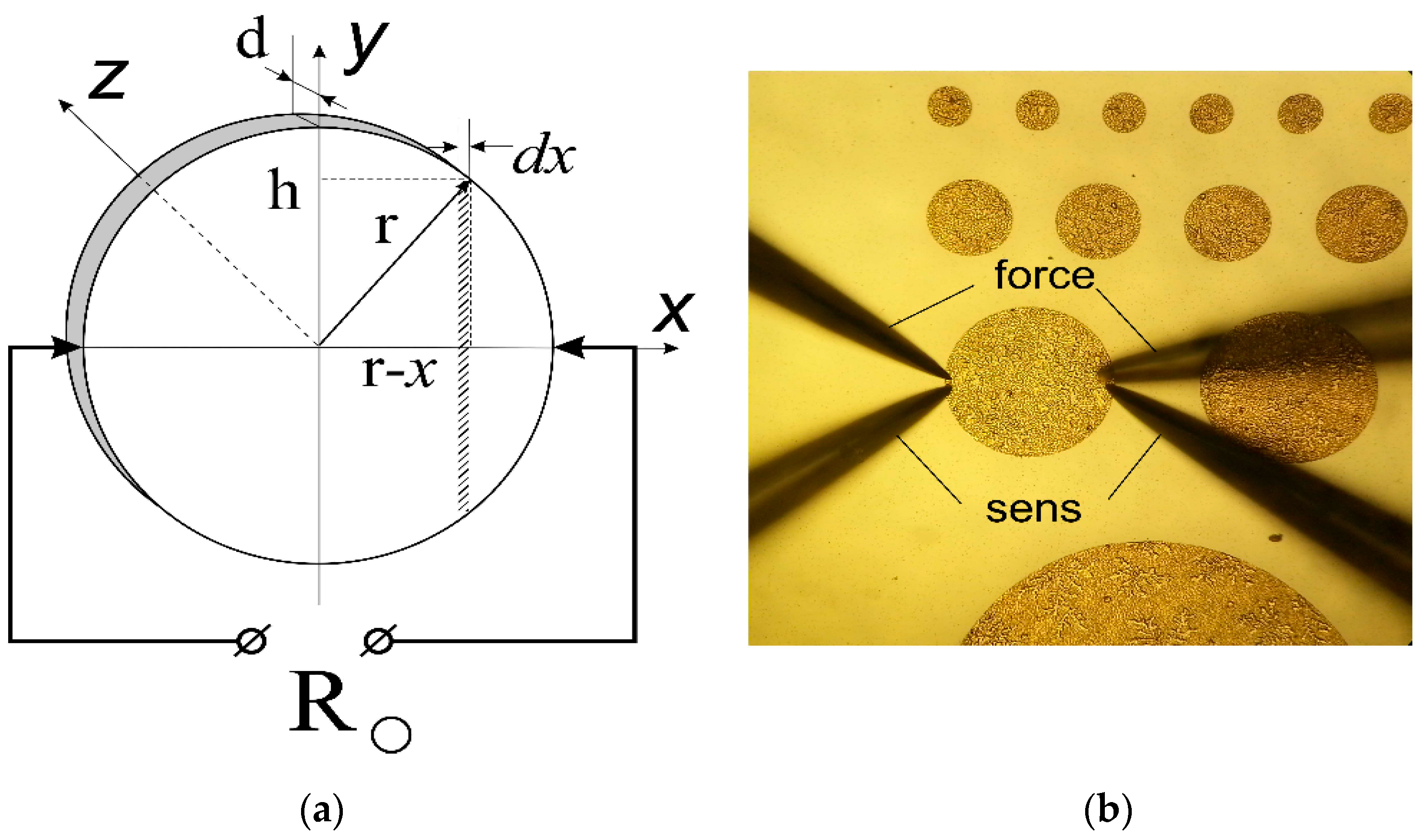
The notion of sheet resistance is often used to characterize electric resistance of thin metal films and systems based on them, when their lateral dimensions on the (
x,y) plane of the film are much greater than the thickness. Sheet resistance can be defined as a resistance of a square
Rsq, i.e., a resistance of a square
R▯ or round
RO (
Figure 1) area of the film.
In this paper, the sheet resistance Rsq of the multilayer metal system TiAlNiAu with the layer thicknesses of 50 × 50 × 150 × 100 nm correspondingly, formed on semi-insulated buffer layer i-GaN is investigated with the use of round TiAlNiAu test contacts with the following values of the radius ri: r1 = 20 um, r2 = 50 um, r3 = 100 um, r4 = 200 um, and r5 = 500 um. The contacts were formed by means of standard lift-off lithography and electron-beam sputtering. Samples were exposed to a fast-thermal annealing with the mode used to form ohmic contacts to nitride HEMT structures in the temperature of 780 °C during 30 s. The measured average thickness of the metal test samples after the annealing was d = 310 ± 60 nm.
Sheet resistance of the test
RO (or conductivity
G = 1/
RO) was measured by the analyzer B-1500 Keysight Technologies at the probe system M-150 Cascade Microtech. The 4-point probes Kelvin method was used to eliminate the influence of serial resistances formed at test surfaces by measuring probes (
Figure 1b). The tolerance of resistance measurement was not more than 0.04 Ω in a bias range from −5 to +5 V.
Thin films with thickness
d(
x,y) = Const and volume resistivity
ρ(
x,y) = Const ([
ρ] = Ω × m) have the following property: the lateral conductivity (resistance) of their square
R▯ and round
RO areas does not depend on their lateral linear dimensions, i.e., on the value of side
a (
R▯(
a) = Const) or radius
r (
RO(
r) = Const) (
Figure 1). Replacing
we can write:
where in
.
Brownian surface irregularity h(x,y) monitoring of the TiAlNiAu test contacts was conducted by means of the optical microscopy.
We used the notions of measure, metric, metric, and normed functional (linear) space to investigate the relation between TiAlNiAu test geometry and resistance RO that allow considering scalar and vector values, continuous functions, and number sequences from a unified position.
In general, measure
M of the measured object is an integral of some function determined at family of Minkowski space sets. It must have the property of additivity and satisfy the axioms of triangle, symmetry and zero spacing [
38]. The Minkowski space is a 4D pseudo-Euclidean space of signature {1,3}.
The definition of the object measure
M involves determination how many times
N the measured object enclosed in the space
with the dimension
D can be filled with some measuring (calibrating) object defined by the function:
(i.g., interval (
D =
DT = 1), square or disk (
D =
DT = 2), cube (
D =
DT = 3)). Here,
DT is a topological dimension of the 1D, 2D, or 3D Euclidean space represented by an integer number,
γ is a normalizing index, and
δ < 1 is a non-dimensional scale.
Then, according to [
39]:
where in general,
DH is a dimension of Hausdorff-Bezikovich space [
39].
In the most cases known today, only non-negative functions defined at families of Minkowski space sets, as mentioned above, are considered to determine fractal measures M. For example, intervals are used to measure a line (1D object), squares are used to measure an area (2D object), and cubes are used to measure a volume (3D object).
This approach enables investigation of object geometry peculiarities but does not allow revealing the connection between geometry and electrophysical properties of the object.
Let us consider metric spaces R formed by pair R = {X, ρ} consisting of some element set X = {x
i} in which distance ρ between any pair of elements is defined with the axioms of triangle, symmetry and zero distance [
38,
40], as the Minkowski space sets. Therein, single-valued, non-negative, and real function ρ = ρ(
rij) has to be defined for any
rij (where
rij is a radius vector between any two
i-th and
j-th points (elements), where
i≠j,
i = 1, 2, …,
N,
j = 1, 2, …,
N, N is a quantity of elements) from the set
X.
For example, the metric space of the thin film system under investigation R = {X, ρ} can be formed by the set X of surface (relief h(x,y)) points, or its components: grains, crystallites and dielectric interspaces, between any pair of which the distance ρ is defined with the axioms of triangle, symmetry and zero distance.
In the meantime, it is known that it is possible to determine various metrics at the same set that are described by certain continuous functions defined at this set. The sets of such functions form functional spaces. For convenience, when functional spaces are considered, geometric notions and definitions are often used. Accordingly, it is possible to use various additive functions to define measure, if they are determined at some being in use normed linear space (hereinafter referred to as a functional space) and their set satisfies all axioms of the linear space [
41]. For such spaces the notions of continuity and norm, which is the equivalent distance between two points in Euclidean space, are applicable. The distance between the functions
F1 and
F2 from the functional space is understood as a norm ||
F1-F2||. Elements of functional space can be presented by various mathematical objects: scalar numbers, vectors, matrixes, singular self-similar (fractal) functions, and self-similar (fractal) sets [
42]. It is very convenient when it is necessary to describe not only spatial but also other properties of fractal objects. For example, an area can be characterized not only by area units but also by dopant area density, various defects area density, electric charge density, etc., which are described both by positive and negative functional dependencies.
Using singular self-similar functions in various functional spaces for process describing is strictly limited in modern electronic (e.g., semiconductor) technologies. Until quite recently, self-similar measure applications in semiconductor material science basically were connected to the statement that all processes taking place on surfaces, interfaces, and in the depth of electronic device were driven by homogeneity of the space, and present inhomogeneities were basically exception and defined by defects, dopants, and anisotropy properties in some cases (e.g., anisotropy of crystal lattice properties). In fact, semiconductor material can have non-linear properties too [
31,
32,
33,
34].
Generically, there is no universal functional space that is why in every individual case depending on the problems considered it is necessary to use the functional space which nature is defined by the class of functions used (metric type) to describe some electrophysical characteristic of the object.
Please note that functions describing average values of resistances R, as well as of many other electrophysical characteristics in electronic technologies, are not fractal. The fractality appears only after introduction of space coordinates (x,y,z) that in fact allows quantitative description of various size effects.
Let us use a functional space consisting of continuous functions F(x,y,z) defined at some area of Euclidean space and describing the dependency of sheet resistance Rsq of the thin film metal system under investigation on coordinates.
Integrals of
F(
x,y,z) are considered to be a measure
Mk = Rsq = Φ in such functional space (functional
Φ):
The functional and metric spaces can be associated by means of mapping every area from the metric space set R to some functional Φ from the functional space Mk, or measure Mk describing some k-th additive (integral) electrophysical characteristic, where k = 1, 2,…K is a quantity of additive characteristics, Mk = {Mki}. In this case, all arguments of the functions F in linear space Mk have to belong to the metric space set R.
Therefore, any i-th element from the metric space set R can be mapped to an integral measure Mki (functional) from the functional space describing some k-th additive (integral) electrophysical characteristic, where k = 1, 2, … K is a quantity of measures.
For example, the space of resistances Mk = 1 = {Rsqi}, masses Mk = 2 = {mi}, electric charges Mk = 3 = {Qi}, etc., can be considered to be such integral characteristics of thin film system functional space elements.
The association of R и
Mk bears a metric space with a measure
SM,k = {R,
Mk} that is an assembly of elements of metric space R on which some set of measures
Mki from the linear functional space
Mk depends (through the arguments) [
38]. Such space already characterizes a specific object along with its properties. In this case, the dimensions of metric spaces R and functional spaces
Mk can stay within topological dimensions of Euclidean spaces as they can be expressed by any real number from 0 to 3.
For example, the integrals of the function of electric charge density, the function of electric current density, or the function of mass density can be regarded as the measures qualifying capacitive, conductive, and weight-size parameters of linear lines, 2D surfaces, and 3D volumes. As opposed to the metric space R, measures of the functional space (functionals Φ) can have, as is stated above, negative values, e.g., as electric charge measures do.
Therefore, the set X of test contacts belongs to the metric space R = {X, ρ}, and the set of the measures {Mki} (the parameters characterizing these contacts), belongs to the functional space.
In the experiments given, i = 1, 2, 3, 4, and 5 (N = 5, five test elements) and k = 1, as we considered just one measure M1i of the only electrical characteristic RO. So here and elsewhere we eliminate subscript k and assume M1i ≡ Mi = ROi, M1 ≡ M, and SM = {R, M}.
For determination of the metric space Harsdorf dimension
DH of the samples under investigation, we used technique based on defining similarity dimension
DS by means of calculation of the object measure
M relative increase in
η =
Mi + 1/
Mi times at measuring scale linear dimensions relative decrease in
ζ = li/li + 1 times [
39].
For this purpose, we traced bitmaps of surface reliefs for the thin film contacts under investigation at given measuring scale li, and counted the obtained number of closed contours of filled areas. At the first iteration, the value of measuring scale l0 was equal to the radius of test contact r, and the obtained number N0 of non-crossing closed contours of zero-level was counted. At the next iteration, the value l0 decreased to l1 in such a way so that after the tracing we obtained the integer number N1 > N0 of the contours enclosed by the contours of zero-level, and so on, until li was equal to minimal distance between image pixels. The maximal number N of enclosed contours corresponding to the minimal value l was chosen as a measure for the metric space of the object M. The value of the similarity dimension DS of the surface metric space at the i-th similarity level can be determined by means of substitution of the values ζ = li/l0 and η = Ni into the Expression (5).
Minkowski dimension
DM, similarity dimension
DS, and Hausdorff dimension
DH are similar in meaning with the following correction
DT:
For linear elements DT = 1, for 2D elements DT = 2. For simplification of physical representation, it is worthwhile to assume that the fractal dimension Df is equal to DM.
In accordance with a Mandelbrot criterion, the value Df for fractal objects have to be greater than the value of Euclidean space topological dimension DE = DT.
According to [
35,
43], the dependency of fractal object measure on its linear dimension
li can be expressed by the following statement:
In the case of limit transition from local approximation to a global one, when the values
Df and
DT are the same, the Expression (7) is converted to a known one for the objects with the integer topological dimension value:
Since the basic properties of metric spaces (properties of triangle, symmetry, and zero distance) can be inherent to functional space elements (functionals) under consideration, it is possible to use Expression (5) to determine their dimension, where the test contact minimal sheet resistance
RO,1 = 0.36 Ω is chosen to be equal to
M0, and the test radius value
r1 = 20 um is chosen to be equal to
l0. Assuming
η = Mi/M0 and
ζ = li/l0, Expression (5) gives the sheet resistance functional space values
DS [
35].
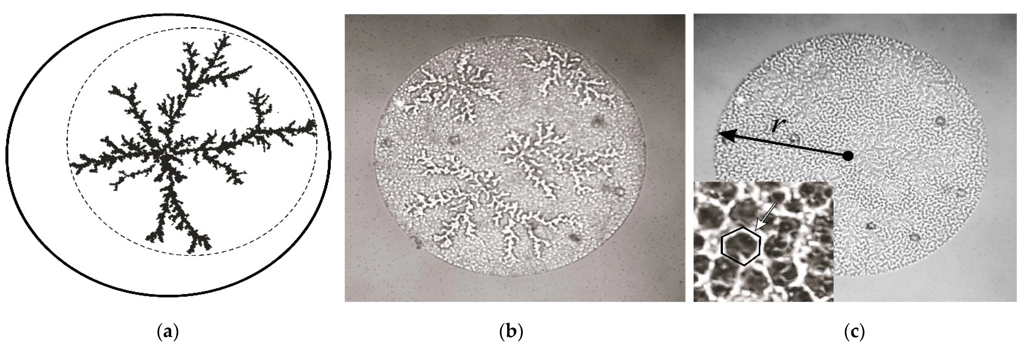
The fractal structure modeling of the crystallites was conducted with the use of off-lattice modeling by means of multiparticle Monte-Carlo technique. In the model experiments we used an assembly of 30,000 Brownian particles. The algorithm of the multiparticle Monte-Carlo technique had the following sequence. During the time
τ, the model particles of the assembly drawn at random from the points of a nontransparent closed contour accomplished one-by-one discrete movements Δ
r inside the contour at the (
x,y) plane. This contour was represented by a circle (
Figure 2, full line). Then we monitored the elementary (step) movements Δ
r of every particle one-by-one during the time
τ and memorized their positions. Furthermore, the process repeated in the same way for a given number of times
N. After the state analysis, we performed the next time step
τ and so on. In such a manner the shown in
Figure 2b dendrite time evolution during the time
t = τ × N was modeled. For modeling particles movement, the random walk model was used.
The model cluster began to grow from the one or several nucleation centers (nuclei) located inside the contour. The Brownian particles of the assembly contacted the growing cluster and could adjoin some of its areas with a specified probability defining a degree of cluster branching. The degree of branching was determined by several connections per unit of length of its self-similar area components, namely by values of scaling rates η and ζ.
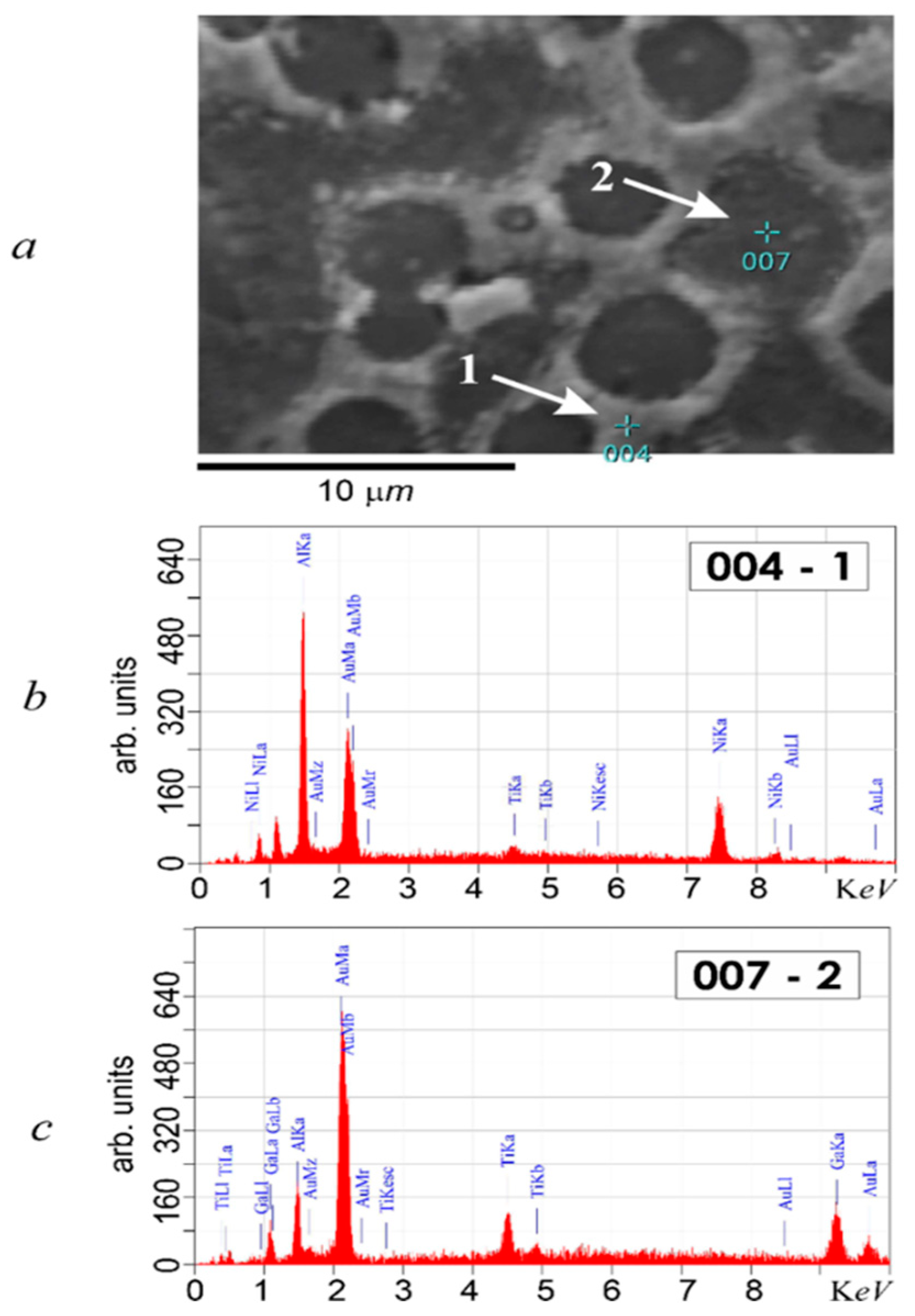
The elemental composition of the tests metallization was determined by means of the analytical high vacuum system with the electron and the focused ion beams Quanta 200 3D (EDAX, Netherlands), fitted out with the system of energy-dispersive analysis (energy-dispersive spectroscopy, EDS) and the X-ray detector Sapphire with the very thin window in the range of energies from 0 to 10 eV at the reduced accelerating voltage of 15 keV.
3. Experimental Results
The measurement of the manufactured TiAlNiAu test contacts of the various diameter reveals that despite the generally accepted conception their sheet resistances
ROi grow with the radius growth from
r1 = 20 um to
r5 = 500 um more than six times, from 0.36 Ω to 2.38 Ω (
Table 1). The size effect observed can be explained by test internal structure peculiarities, as the average dispersion of the thickness
d = 300 ± 60 nm cannot result in such a great difference in sheet resistance values
ROi. The possible reason of the dependency of
ROi on the radius
ri is seen to consist of substructure inhomogeneity of the tests, namely in its fractal constitution.
From the analysis of test surfaces bitmap images, it follows that the space between the dendrites grown in 2D plane in TiAlNiAu thin film system is filled up by a mesh structure (
Figure 2c, insertion, pointed with an arrow), which looks like hexagonal Benar meshes. The mesh lateral dimension does not depend on the test contact radius and equals 4 ± 0.5 um on average.
A dendrite lateral dimension was determined on the basis of the radius of its circumscribing circle (
Figure 2a, dotted line). Unlike meshes, the dendrite lateral dimension grew as
ri increased in a raw: for
r1 it was equal to 18 um, for
r2—53 um, for
r3—61 um, for
r4—140 um, and for
r5—275 um. It is known that such dendrites appear as the result of 2D limited diffusion of particles aggregation [
39].
The investigation of the contour map of the tests surface (
Figure 2b) allows defining the value of the dendrite’s similarity dimension
DS as
Ds ≈ 1.66 (5) that is virtually equal to their computer model value
Ds ≈ 1.63. The fractal values 1 <
DS < 2 of linear dendrites points out that because of their branching in a plane of the contact some 2D properties are inherent to them too. The obtained in the same way values 2 <
DS < 3 of 2D mesh structure point out that apart from 2D properties some bulk properties can be inherent to it [
39].
In accordance with the EDS analysis of the tests, their elemental composition has inhomogeneous lateral spreading that almost completely correlates with their metallization morphology. Therefore, as per spectrums shown in
Figure 3b, the mesh dendrites and walls are formed by the initial set of the elements Ti, Al, Ni, and Au (
Figure 3b, point 1). As per
Figure 3c, the point 2, and the data [
4], the exit of Ni from the meshes during the rapid annealing results in its redistribution and the aggregation of the Ni-Al conductive alloy in the areas of mesh dendrites and walls localization. At this, the retention of the diffusive Ni barrier at these areas during the annealing almost completely preserves the top contact layer of the golden phase.
The absence of the diffusive Ni barrier inside the meshes and the space between the dendrites during the annealing (
Figure 3c, point 2) results in their filling with the low conductivity Au-Al system which promotes a strong growth of these areas electrical resistance and expenditure of significant part of the Au top contact layer.
From
Figure 3, it follows that region 1 at the cell boundary has an increased content of the Au phase and, for this reason, better conductivity. The cells are formed by wall irregularities with a thickness of 30–50 nm at the base and a height of about 300 nm. In general, as can be seen from
Figure 2b,c, the cells form a fractal structure in the metallization plane, which determines the dependence of the layer resistance on the linear dimensions of the film (9). Observed in
Figure 2b, dendrites stand out against the general background (
Figure 2c) due to the fact that the formed cells have a high wall height of 450–550 nm.
In this way, high conductivity of the mesh dendrites and walls at low conductivity of the space between them, as well as good compliance of their fractal parameters with the same parameters of the sheet resistances linear space, can explain the dependency of the tests sheet resistance on their lateral dimensions.
In accordance with (7), the relation of tests sheet resistance
Rsq and their linear dimensions can be represented by the following power-law dependencies:
The Expression (9) describe also a case of limit transition from the local approximation to a global one when the values Df and DT match and Rsq does not depend on linear dimensions of measured areas: R▯,i = R▯,0 and RO,i= RO,0.
We remind readers that a fractal crystallite (dendrite) differs from a usual (non-fractal) one due to the fact that its density decreases exponentially as the distance to its center increases [
39]. In this case, the similarity dimension
DS or fractal dimension
Df can play the role of the power in (9). They are quantitative characteristics of non-uniformity of topological space crystallite filling at the plane [
39]. The decrease of fractal crystallite density with the increase of the distance to its center is ascribable to a growth of its components branching in a space that in accordance with their equivalent electric circuit, is accompanied with the power-law increase of the resulting electrical resistance. At this, the growth of crystallite branching is accompanied with the expansion of its boundaries and consequently with the widening of dielectric spaces between neighboring crystallites. It results in conduction electrons additional scattering at these boundaries and, according to the Mayadas-Shatzkes conductivity model, tests sheet resistances growth with their linear dimensions increase that we observe in experiments.
Table 1 represents the dimensions
DS(
RO) of all five tests. It can be seen that the average values
DS(
RO) calculated on the basis of the Expression (5) have fractional values that are close to average value
DS of the crystallite metric space. It follows that a power law dependency of sheet resistances
R▯(
O) of the thin film system under investigation is determined mainly by crystallites fractal geometry not by mesh structure.
Consequently, it is possible to conclude that the lateral conductivity of tests is provided mainly by crystallites that have much better conductivity than the Al-Au alloy filling the mesh structure.
The obtained experimental results reveal the existence of self-similarity phenomenon not only between the elements of metric spaces R, but also between functionals, i.e., elements of normed functional spaces that is not obvious. This explains the observed size effects that imply dependency of electrophysical characteristics of the object on its geometry [
31,
35].
In accordance with the data shown in
Table 1, the value of the Hausdorff dimension of functional space
DH is relative and depends on the point of reference (system of coordinates, or the point of view of the observer). This agrees well with the one of the attributes of chaotic systems. In the case when
M0 is equal to the minimal value
RO,0 = 0.36 Ω
DS,1(
RO) have one value, and in the case when
M0 is equal to the maximal value
RO,0 = 2.38 Ω
DS,2(
RO) have another value (
Table 1). In accordance with the obtained results this relativity of
DS values does not generate contradictions in determination of measures
M of the object under measurement as in accordance with (7) the value
M is invariant with respect to the values of
M, l, and
Df, i.e., does not depend on the point of view of the observer.
The same size effects were found out in a thin film AuGeNi metal system used to form ohmic contacts to GaAs with an electron conductivity type [
44].


 and
and 


