1. Introduction
Careful design of functional blocks, nodes, and components is required for the successful operation of radio-electronic equipment (REE) [
1]. It is also necessary to control the levels of electromagnetic interference for the correct operation of critical REE in compliance with the requirements of electromagnetic compatibility (EMC), and to assess their danger and possible failures in the operation of REE. Issues with functional safety with regard to EMC have been studied for a long time [
2,
3,
4,
5]. Ultra-wideband (UWB) electromagnetic interference is a particularly dangerous type of electromagnetic interference [
6,
7]. The main sources of such interference can be powerful transmitting or switching devices [
8]. Due to their high power and wide spectrum, UWB pulses can lead to REE failure, damage or disruption [
9]. Critical systems (e.g., those that are deployed in space or aviation) require REE components to be carefully designed and to take into account the EMC standards [
10]. Modeling methods must also be carefully selected. Thus, for example, the relevance of improving the modeling of radiated EMC coupling onto a multilayer printed circuit board (PCB) was considered [
11]. At the stage of early design decisions, it is advisable to focus on qualitative and quantitative assessment of critical «weak points».
Since reliability is a decreasing function of time, the probability of failure of critical systems gradually increases with time. To increase the reliability of critical REE, it is necessary to apply redundancy to its most vulnerable circuits [
12]. The main idea of redundancy is that additional devices and capabilities are employed in order to maintain the working efficiency of electronic equipment if one or more of its elements fails. However, the cost and reliability of the system is directly dependent on the number of redundant parts (
Figure 1). Controlled structural redundancy was proposed to increase the fault tolerance of a control device, a key component in a microsystem [
13]. A number of papers have addressed the problem of redundancy distribution in serial–parallel structures. An approach that combines hot and cold redundancy was proposed in [
14]. However, it is important to keep a balance between cost and performance in the systems that use this approach. In [
15], the problem of redundancy distribution with a cold redundancy strategy in non-recoverable systems is considered. Heterogeneous fault-tolerant systems with a combination of hot and cold redundancy are also discussed in [
16]. In such systems, the method of distributing elements between redundant and primary units, as well as the switching order, can significantly change the reliability and cost of the system. An approach to improve the reliability of a high-voltage modular multilevel converter by implementing redundancy was suggested in [
17]. Thus, it can be concluded that redundancy is a well-known way to increase reliability. However, a significant disadvantage of such solutions is that when there is no need to switch to the redundant equipment, redundancy is not involved in any way.
Modal reservation (MR) is a promising type of cold redundancy [
18]. With the use of MR, strong electromagnetic coupling is formed between the primary (reserved) and redundant (reserving) circuits. This coupling allows for the use of modal distortions in the line to protect REE from UWB pulses [
19]. A schematic diagram with a single MR is shown in
Figure 2a. In this diagram, a short-duration excitation pulse applied at the input of the reserved circuit is decomposed into two unipolar pulses at its output. At the same time, two pulses of opposite polarities are formed at the output of the reserving circuit. With a single MR, the reserved and reserving circuits are arranged symmetrically relative to one of the planes. There are some studies that consider protective electrical circuits with a single MR [
20,
21], the UWB pulse attenuation after a failure with a single MR [
22], or conduct a multivariate analysis of structures with a single MR [
23]. The multivariate analysis considered the deviation of the maximum voltage amplitudes at the output of the reserved conductor obtained for protective circuits without failures and for protective circuits with failures. Taking into account the nature of UWB interference, the authors in [
24] revealed that the probability of failure in the reserving equipment is lower than that in the reserved one.
To increase reliability by means of greater duplication and better noise reduction, protective electrical circuits with a triple MR were proposed in [
25]. A schematic diagram with a triple MR is presented in
Figure 2b. If the UWB pulse excites the input of the reserved circuit, then at its output it will decompose into four unipolar pulses of smaller amplitudes. At the same time, four pulses of different polarities are formed at the output of the reserving circuits. Their waveforms and amplitudes depend on the electromagnetic coupling coefficients between the conductors, as well as the reflection coefficients of the modes. The equality of the amplitudes of the decomposed pulses is achieved at a certain coupling between the conductors. The arrangement of the conductors when the reserved and reserving circuits are located symmetrically relative to two planes is most appropriate. Such symmetry of protective electrical circuits with a triple MR has a number of advantages, for example, it provides easier and faster optimization of the cross-section parameters. When a UWB pulse excites one of the circuits with a triple MR, the symmetry of conductors and terminations of the circuits enable its equal suppression. However, with an extremely powerful UWB pulse, there is a risk of failure of both reserved and reserving equipment. Previously, the characteristics of protective circuits with a triple MR, represented as multiconductor transmission lines, were considered in [
26]. The optimal switching order after failures in a multilayer structure with a triple MR was investigated in [
27]. In [
28], the efficiency of MR in the circuits of a spacecraft autonomous navigation system was evaluated. However, the above-mentioned works have not addressed the assessment of the risk of disabling reserved and reserving equipment in symmetric protective circuits with a triple MR. Meanwhile, pulses of different polarity can damage electronic equipment connected to reserving circuits. This may result from the different nature of the impact caused by unipolar and bipolar pulses on the protected equipment. Thus, the purpose of this work is to assess the threat of disabling reserved and reserving equipment in a symmetrical protective electrical circuit with a triple MR.
This paper is divided into five sections.
Section 2 describes in detail the approaches, methods, and materials used, as well as the device under investigation.
Section 3 presents the results of quasistatic simulation and experimental study. The results are discussed in
Section 4, followed by the conclusion in
Section 5.
2. Materials and Methods
This section describes the structure under investigation, approaches to its simulation, as well as the methodology of its experimental study. The limitations of the study are given at the end of the section.
2.1. Structure and Materials
In this paper, the authors investigated a symmetric structure with a triple MR from [
25], the cross-section of which is shown in
Figure 3. The structure is a four-layer PCB, the core of which is Rogers RO3010 laminate, and the pre-preg is FR-4 fiberglass. The reserved and reserving conductors are located symmetrically on the inner layers of the PCB. The outer layers are solid polygons which are reference planes (circuits ground). They are interconnected by jumpers at the near and far ends of the structure. The geometric parameters of the line are as follows: the width of the conductors (
w) is 185 μm, the distance between the conductors (
s) is 315 μm, the thickness of the conductors (
t) is 35 μm, the thickness of the core (
h1) is 130 μm, and the thickness of the pre-preg (
h2) is 600 μm. For the core, the relative dielectric constant (ε
r) is 10.2, and the tangent of the dielectric loss angle (tgδ) is 0.001; and for the pre-preg, these values are 4.3 and 0.025, respectively. The length of the entire structure (
l) is 324 mm.
The PCB of the structure with the triple MR and its internal layers are shown in
Figure 4. The board consists of many circuits with single and multiple MR, but they are not used in this study. The upper inner layer of the PCB is shown in red, and the lower one is in blue. The footprint holes for the signal contacts of the coaxial-to-microstrip transition KLS1-SMA001 are marked in black, and the ground contacts are white. The ground contacts allow the measured equipment to be connected to any conductor at both ends.
2.2. Simulation Approaches and Methods
To obtain the characteristics of the structure with MR in the time domain, the authors used a quasistatic analysis in the TALGAT system [
29]. The system is designed to simulate a wide range of EMC problems, including calculating the time response of multi-conductor transmission lines. The accuracy of the methods used in TALGAT is confirmed by the consistency of the results obtained with the quasistatic and electrodynamic approaches [
30], as well as the results of the experimental study [
31]. In the quasistatic analysis, the structure under investigation was represented as a straight line and with a constant cross-section along its entire length. The method of moments was used to find the matrices of per-unit-length coefficients of electrostatic (
C) and electromagnetic (
L) induction, as well as resistances (
R), and conductivities (
G) [
32]. In this case, the boundaries of the conductors and dielectrics in the PCB cross-section were divided into segments with a length of no more than
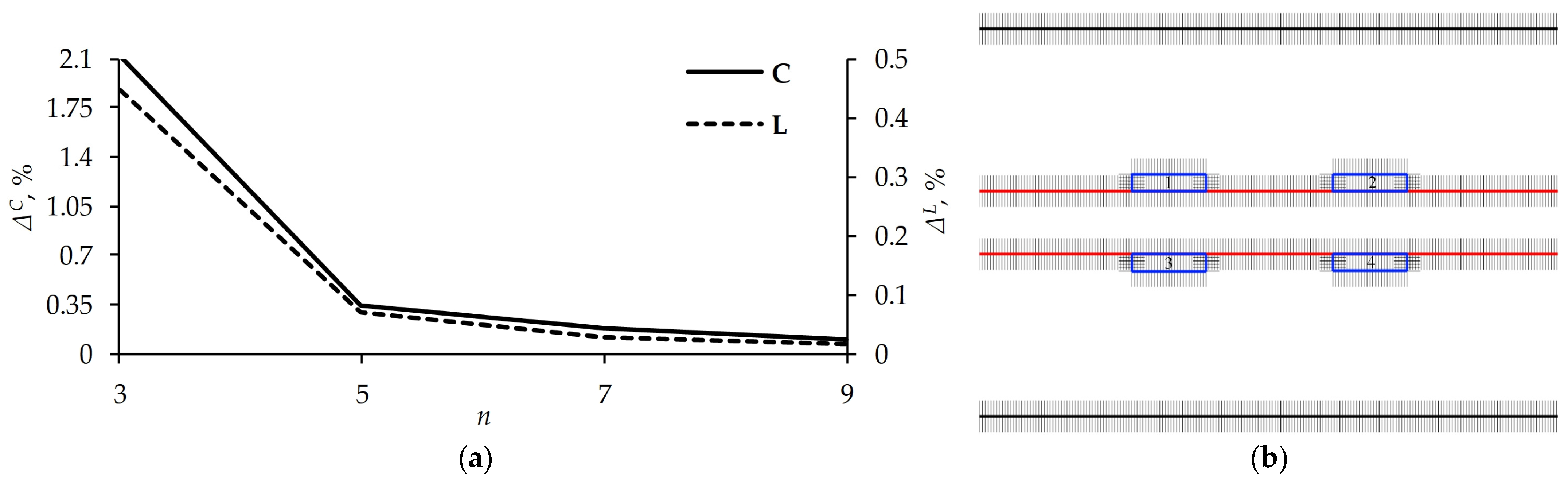
t. Since the accuracy of the calculations depends on the number of segments, it is necessary to find their optimal value. For this, the convergence of the relative deviations of matrices
L and
C was estimated for different segmentation
using matrix norms:
where
is the Frobenius norm and
n is the number of segments at the edges of the conductors (
n = 3, 5, 7, 9). As shown in
Figure 5, the deviation of matrices
L and
C with five segments at the edges of the conductors is less than 0.35%, and with increasing segmentation the deviation tends to 0. Thus, the segment length in quasistatic modeling is taken to be equal to 7 um. It is important to take into account the frequency dependence of the electrical characteristics of the materials used during the time response simulation of the PCB. Therefore, in the quasistatic simulation with losses, the frequency dependence of ε
r and tgδ of FR-4 from [
33] was applied.
A trapezoidal excitation source simulating a UWB pulse was connected to the input of the reserved conductor (node V1). The front, the fall, and the flat top were 20 ps each, and the amplitude was 2000 V. The authors used such a pulse because it is easy to analyze it in lossless simulation. The waveform of the pulse makes it easy to determine the arrival times and amplitudes of the decomposition pulses. A short duration of the pulse is also suitable for complete pulse decomposition. In order to match the transmission line with the source, the resistors R1–R8 are assumed to be equal to 50 Ω.
The voltage waveforms were analyzed at the output of the reserved and reserving conductors (nodes
V2,
V4,
V6,
V8). To analyze how significant the influence of unipolar and bipolar pulses on electronic equipment and components is,
N-norms were used [
34].
Table 1 shows the analyzed norms and their characteristics that were taken from [
35]. They can be used to assess the possibility of electrical breakdown in a dielectric, burnout of an electronic component, etc. The voltage waveform of the decomposed pulses
U(
t) is used in the formula as an argument.
2.3. Experimental Technique
To confirm the results of quasistatic simulation, we carried out an experimental study.
Figure 6a shows an experimental setup consisting of a DSA8300 digital stroboscopic oscilloscope (1), a discrete 80E04 module (2), microwave cables (3), matching loads (4), and a PCB with a triple MR (5). At the first stage, a pulse with a linearly increasing front was exciting the input of the reserved conductor (node
V1) using a discrete module, and responses were observed at the output of the reserved (node
V2) and reserving conductors (nodes
V4,
V6,
V8). The time step in the waveform measurements was 1.25 ps. To minimize the measurement error, the maximum permissible resolution of the stroboscopic oscilloscope along the voltage and time axes was set. The measurements were carried out sequentially from one node to another, while all coaxial-to-microstrip transitions were loaded at 50 Ω to coordinate with the measuring path. At the second stage, to smooth out small fluctuations and outliers, a moving average function was applied to the waveform
U(
t). The number of averaging points was assumed to be 20. At the third stage, taking the derivative of the time responses to the stepwise pulse
U(
t), we obtained time responses to the function d
U(
t)/d
t (see
Figure 6b). Since the device under study was linear, for ease of perception, the scale of the resulting waveforms was normalized to 1 V.
Figure 6c shows the voltage waveforms of the input pulse, which are used later in the analysis, with a linearly increasing front and its derivative. In this case, the sum of the durations of the front, fall and flat top of the resulting pulse is equal to the duration of the front of the input signal Δt. As in the case of the responses obtained during quasistatic simulation, we analyzed the
N-norms of the voltage waveforms at the output of the reserved and reserving conductors.
2.4. Limitations of the Study
In the quasistatic simulation, it was assumed that only transverse T-waves propagate in the transmission line. The waves of higher orders were not taken into account. Thus, their influence was not observed in the time response. In addition, when comparing the simulation and experimental results, discrepancies in the arrival times or maximum attenuations of pulses may be caused by insufficiently accurate εr and tgδ values of the dielectrics, as well as their frequency dependences. At the same time, the insertion losses and the delay of coaxial-to-microstrip transitions should be taken into account. When analyzing N-norms, the obtained results should be correctly interpreted since, without a real object to be protected, they can only give a relative assessment of the significance of the impact. To quantify the probability of equipment damage or failure, it is necessary to take into account, among other things, the design and circuit features of the components and of the whole REE. In the case of decomposed pulses obtained during the experiment, digital averaging operates as a low-pass filter. Despite the small averaging value, the high-frequency components of the UWB pulse may be lost. An additional measurement error is provided by the measuring unit.
3. Results
This section presents the results of the theoretical analysis, quasistatic simulation, and experimental study of a symmetric structure with a triple MR.
3.1. Theoretical Analysis
In this section, the structure under consideration (
Figure 3) is represented as a lossless four-conductor transmission line in an inhomogeneous dielectric filling. According to the theory of multiconductor transmission lines based on modal analysis [
36], for this symmetric structure, in the general case, there are four linearly independent vectors, the absolute values of which are equal. The square matrix for the structure in
Figure 3, where the columns represent the eigenvectors of the voltages, has the form:
Further, to calculate levels of the decomposed pulses, provided that each mode is matched (i.e., there are no reflections in the transmission line), the following expressions were used:
where
V is a matrix of
size, the elements of the rows of which contain the amplitudes of the decomposed pulses;
e is a vector of
size, consisting of the values of the amplitudes of the voltage sources.
The calculation of the amplitudes is performed when an e.m.f. source with an amplitude of 2000 V is connected to the reserved conductor. The column vector
e and the calculated matrix
V have the following values:
The
V row element values show the amplitudes and polarities of the decomposed pulses at the output of each conductor. Row 1 corresponds to the reserved conductor (node
V2 in
Figure 2b), and rows 2, 3, and 4 correspond to the reserving conductors (node
V4,
V6, and
V8 in
Figure 2b). In this case, the combinations of polarities and amplitudes of the decomposed pulses do not depend on which input node the e.m.f. source is connected to.
To analyze the voltage waveforms of decomposed pulses, the authors further performed a quasistatic simulation with and without losses in the conductors and dielectric.
3.2. Quasistatic Simulation without Losses
Appendix A and
Figure A1 show the voltage waveforms at the output of the reserved and reserving conductors under the excitation of the UWB pulse at the input of the reserved conductor. These results were obtained in the quasistatic simulation without taking losses into account. Since there are four modes propagating in the structure, four pulses are observed at the output of all conductors. In this case, the amplitudes and polarities of the pulses are consistent with matrix
V. It can be seen that only at the output of the reserved conductor the pulses have the same polarity. At the same time, pulses of different polarity are observed at the output of the reserving conductors; half of them have the opposite polarity.
Table 2 presents the amplitudes and delays of the decomposed pulses, and
Table 3 contains the calculated
N-norms of 0.18 ns. In 0.54 and 0.61 ns after the arrival of mode 2, the pulses of modes 3 and 4 arrive, respectively. The difference between the delays of modes 3 and 4 was 0.055 ns; as a result, a slight overlap of pulses was observed. The maximum modulus voltage at the output of each conductor is determined by mode 2, and it was 242 V. As a result, the amplitude of the UWB pulse acting on the input of the reserved conductor decreased by 4.06 times. It can be seen that its energy is distributed over time. For
N1, the maximum peak value in all considered nodes is the same. Accordingly, it can be assumed that the probability of an electrical breakdown or arc discharge will be the same in all the nodes. The
N2 values decreased by 2.38 times for the
V8 and
V4 nodes and by 3.54 times for the
V2 and
V6 nodes. This indicates that the probability of component arcing in only one reserving circuit is the same as in the reserved circuit. The other two reserving circuits have
N2 values 1.48 times higher than the reserved ones. This result is explained by the fact that the rate of change of the function
U(
t) increases because of the superposition of the positive pulse of mode 3 and the negative pulse of mode 4. The maximum
N3 value is observed at the output of the reserved conductor. At the same time, in the reserving circuits, the
N3 value is less (by 3.74, 2.336, and 4.705 times) than in the reserved one. Therefore, the probability of a dielectric breakdown in the reserving circuits is much lower than in the reserved one. The values for
N4 and
N5 are approximately the same for both reserved and reserving circuits. Therefore, the probability of burnout or damage to a component because of the total pulse energy is approximately the same in all circuits under consideration.
3.3. Quasistatic Simulation with Losses
Appendix B and
Figure A2 show the voltage waveforms in the same nodes but taking losses into account.
Table 4 presents the amplitudes and delays of the decomposed pulses, and
Table 5 contains the calculated
N-norms. Since the delays do not change because of the insertion losses, they correspond to the values from
Table 2. Since the structure under study is a lossy transmission line, a strong dispersion of the decomposed pulses is observed at the output of all conductors. Thus, the pulses corresponding to modes 3 and 4 overlapped. In the case when their polarity is the same, it is impossible to distinguish the time of arrival or the amplitude of each pulse. If these pulses have different polarities, then due to mutual compensation in the places of overlap, the voltage significantly decreases. The maximum modulus voltage at the output of each conductor was 153−155 V. The slight difference is explained by different effects of dielectric losses. As a result, the amplitude of the UWB pulse acting on the input of the reserved conductor decreased by 6.42−6.34 times. According to
N1, the maximum peak value at all considered nodes is practically the same. Slightly lower
N1 values are observed at nodes
V4 and
V8. As in the case of the simulation results without losses, the probability of an electrical breakdown or arc discharge will be practically the same in all nodes. The
N2 values at all nodes are approximately the same. There is no sharp change in the function
U(
t) at the sites where oppositely polarized pulses 3 and 4 overlap. This could be explained by the presence of line losses, which smooth out the decomposed pulses and do so in a different way for each mode. The maximum values of
N3 and
N4 are observed at nodes
V2 and
V6, and the minimum values are observed at
V4 and
V8. This may be explained by the fact that, because of partial mutual compensation of slow modes, the total pulse energy decreases. The
N5 values in all reserving conductors are less than in the reserved ones. However, the difference between nodes
V2 and
V6 is minimal.
3.4. Experimental Results
Appendix C and
Figure A3 show the voltage waveforms in the same nodes obtained in an experimental study.
Table 6 presents the amplitudes and delays of the decomposed pulses, and
Table 7 contains the calculated
N-norms. At the output of all conductors, there are clearly observed pulses corresponding to fast modes 1 and 2. Due to the small difference in per-unit-length delays and pulse dispersion, slow modes 3 and 4 overlap. Hence, it is impossible to distinguish the arrival times and amplitudes of pulses at nodes
V2 and
V6.
In this case, between pulses 2 and 3, there are pulses that were not observed during the simulation. They could have appeared because of the discontinuities of the layout from coaxial-to-microstrip transitions to the section with a triple MR. Since the characteristic impedance of the transmission line in these places sharply changes, multiple reflections appear. In this case, the reflection and transmission coefficients for each mode change from one section to another. The differences between the experimental mode delays and the calculated ones could be primarily explained by the fact that the influence of coaxial-to-microstrip transitions was not considered in the simulation. In addition, the real values of εr and tanδ, as well as their frequency dependences, may differ. The maximum voltages on the module at the output of each conductor were 0.097−0.112 V. As a result, the amplitudes of the UWB pulse acting on the input of the reserved conductor decreased by 10.31−8.93 times. The N1 values differ slightly at all nodes due to the small differences in the transmission and reflection coefficients of modes. As a result, the probability of an electric breakdown or an arc discharge will be approximately the same in all the nodes. When analyzing N2, it was found that it decreased by about 4.03 times. In this case, the N2 value is approximately the same in all nodes, so the probability of component arcing in the reserved and reserving circuits is the same. The N3 value in the reserving circuits is significantly less than in the reserved ones: up to 24 times in the V4 and V6 nodes. The probability of a dielectric breakdown in these circuits is much lower than in a reserved circuit. The N4 and N5 values in the reserving circuits are lower than in the reserved ones: up to 1.39 times at the V4 and V6 nodes. Therefore, the probability of burnout or damage of a component in the reserving circuits is lower than in the reserved one.
5. Conclusions
In this paper, for the first time, the results of the analysis of the N-norms of the voltage waveforms of decomposed pulses in symmetric protective electrical circuits with a triple MR were presented. Previous studies, as well as the results of this work, have shown that this approach to redundancy of circuits and interconnections yields significant attenuation of powerful conducted interferences with short duration. However, in this work, also for the first time, the decomposition of a UWB pulse in reserving circuits was shown experimentally. The results of quasistatic simulation without losses showed that the probability of dielectric breakdown in the reserving circuits is lower than in the reserved circuits. In simulations with losses, the N3 value in the reserving circuits is also lower than in the reserved one. At the same time, in the reserving circuits, the N4 and N5 values are lower than in the reserved ones. This indicates a lower likelihood of burnout or damage to the component.
Meanwhile, an important fact of N2 doubling in the reserving circuits was revealed with a partial overlap of different polarity pulses. However, this overlap showed up in lossless simulations but disappeared in lossy simulations and experiment. Therefore, it is important to investigate this in detail in the future.
The results obtained give relative indicators of reliability. In the future, it is planned to conduct a study that will apply quantitative methods for assessing reliability. So, for example, from the theory of probability, the Poisson point process can be applied. A promising direction of research is to develop models for calculating and analyzing the reliability of systems with MR.
To summarize, the study discussed the effects of symmetry/asymmetry. The proposed protective electrical circuit is symmetrical relative to two planes. As a result, the theoretical analysis of such circuits is greatly simplified compared to asymmetric circuits. This could be explained by the fact that the elements of the SV are equal in modulus. A significant advantage of symmetrical circuits over asymmetric ones is a simpler way of finding optimal parameters. This results from their smaller number in symmetrical circuits. When the source of the UWB pulse is connected to any of the conductors, the same voltage waveforms will be at their output. In this case, two pulses of positive polarity and two pulses of negative polarity are formed on adjacent circuits. In asymmetric circuits, more complex combinations can arise that require careful design analysis.


