1. Introduction
Surface cleaning treatments are the foundation of a semiconductor device fabrication process [
1,
2]. Surface cleaning significantly affects the epitaxial defects [
2], metal contact resistance/stability [
3], and overall device quality of GaN-based devices [
4]. Evaluating surface cleanliness requires considering the electrical properties of the device, structure, and interface state trap of the surface. Moreover, a surface treatment is used to remove the native oxides, organic contaminants, metal ions, particulates, residual species, and weaknesses in atomic bonding.
Recently, AlGaN/GaN high electron mobility transistors (HEMTs) were demonstrated for use in power electronic devices. In an HEMT device, a high saturation current, low leakage current, and high transconductance are necessary. Therefore, a low-resistance ohmic contact and low interface state trap density (
Dit) must be obtained for an HEMT device. Interface states may cause various operational stability and reliability drawbacks in GaN-based HEMTs such as threshold voltage instability [
4] and current collapse phenomena [
5]. A surface treatment not only improves the device performance but also enhances the ohmic contact characteristics of GaN with metals [
3].
In addition, surface treatments have been proposed to improve the ohmic contact properties between a low work function metal contact and a GaN or AlGaN surface. N vacancies are created during surface treatment and act as shallow donors for electrons and increase the surface doping concentration to overcome the Schottky barrier height for carrier transport. Therefore, improving the contact properties and reducing contact degradation are crucial for an AlGaN/GaN HEMT. A poor surface quality causes surface defects and contamination of the interface states, which originate from dangling bonds. The surface chemical treatment is not the only way to improve AlGaN/GaN HEMT device performance. The phosphorus-based annealing processes (POCl
3, P
2O
5) also modified surface conditions before dielectrics material deposition to further modify the AlGaN/GaN HEMT [
6]. The metal-oxide-semiconductor HEMTs(MOS-HEMTs) structure using different dielectrics material causes different device performance of MOS-HEMTs, such as different C–V characteristics, specific resistance (R
on), breakdown voltage,
Dit value, saturation drain current of the devices [
7]. The MOS-HEMTs structure using Al
2O
3 [
8] will be effective to enhance the breakdown voltage generated from the gate leakage. The ALD is a surface-controlled layer-by-layer process for the deposition of thin films with atomic layer accuracy. The Al
2O
3 used for MOS-HEMTs not only improve the basic electronic properties but also show low leakage current and high breakdown voltage. In this study, four chemical pretreatments were used for MOS capacitors before atomic layer deposition (ALD) of Al
2O
3 to modify the surface quality. The characteristics of MOS capacitors and the ohmic contact characteristics of GaN with the four chemical treatments are discussed.
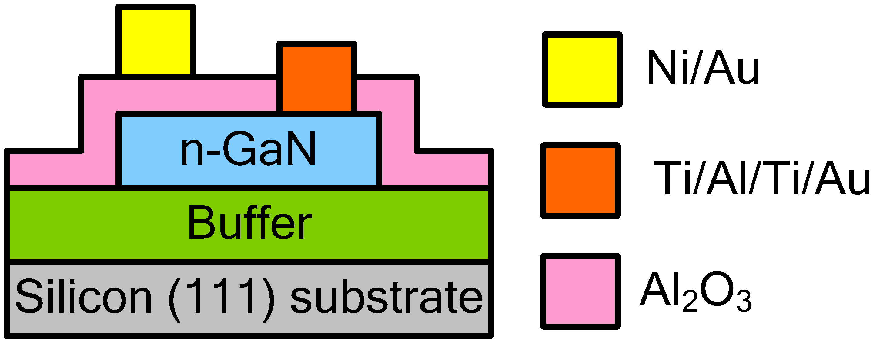
3. Results and Discussion
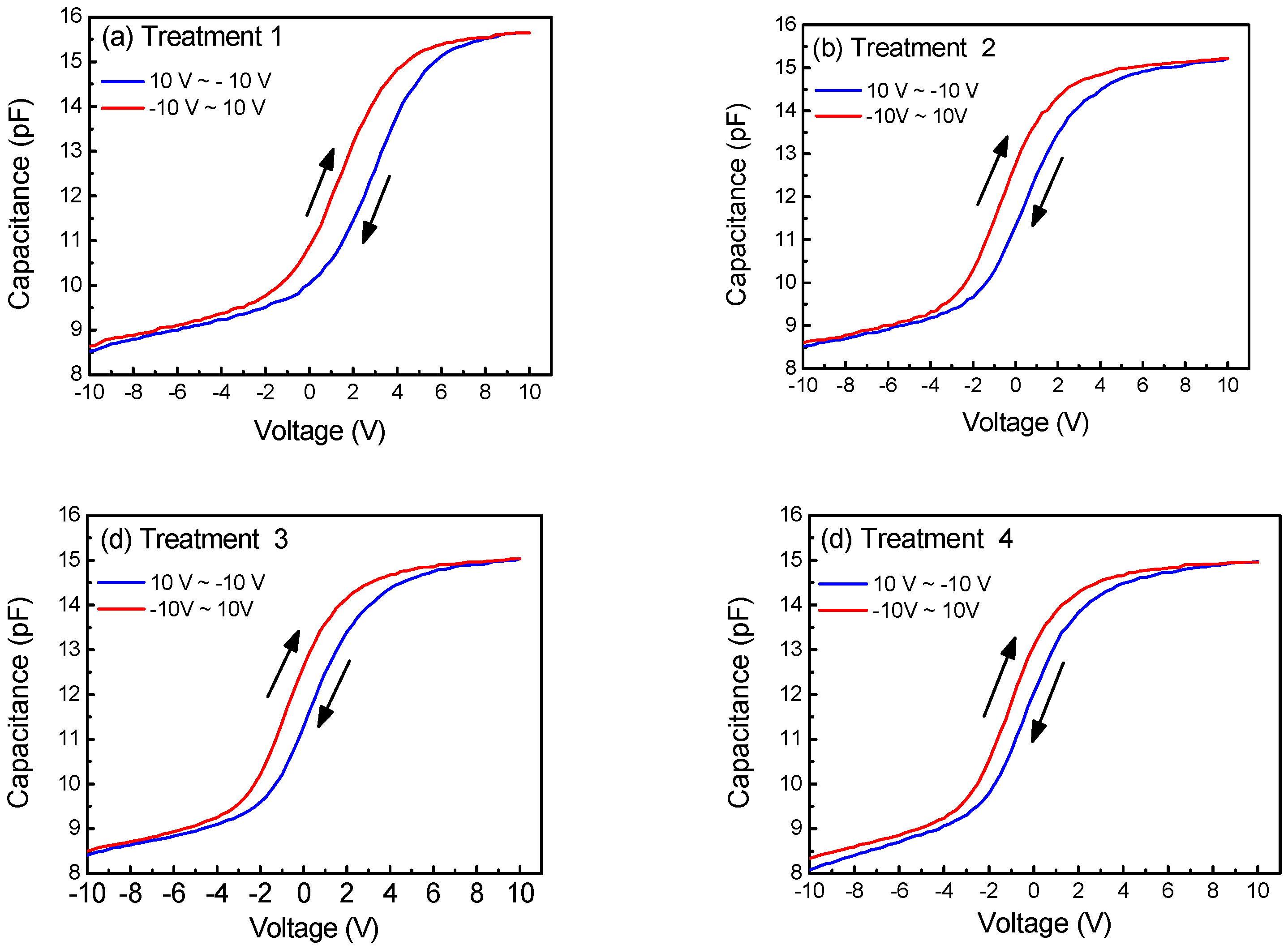
The hysteresis behavior of capacitance–voltage (C–V) curves is strongly correlated to the trap density at the GaN/Al
2O
3 interface of a MOS capacitor.
Figure 2 shows the hysteresis behavior of the C–V curves of MOS capacitors treated with various chemical treatments. Obviously, the MOS capacitor treated with treatment 1 exhibited the largest amount of hysteresis. Treatment 1 consisted of an organic solvent and O
2 plasma, which were used to remove particles from the air ambiance, and stripped residual photoresist and organic contaminants. The dangling bond, weaknesses in atomic bonding, and native oxides are difficult to remove using treatment 1. Generally, they are removed by complexes composed of organic and inorganic solvents, such as treatments 2–4.
To calculate the
Dit value, the oxide capacitance (capacitance at accumulation,
Cox) was measured using the C–V curves. The flat band voltage (
VFB) was calculated using Equation (1) to quantify the relative shifts for analyzing the hysteresis behavior of the capacitors;
VFB was measured using the C–V curves at a point of
CFB obtained using [
9]:
where
εs = 9.5 is the dielectric constant of GaN,
λ = (
εsε0kBT/
q2ND)
1/2 is the Debye length of n-GaN [
10],
T is the absolute temperature,
q is the electron charge,
kB is the Boltzmann constant, and
ND = 6 × 10
17 cm
−3 is the electron concentration of n-GaN. The relative shifts in
VFB during the sweep down (10 to −10 V) and up (−10 to 10 V) for the surface treatments of GaN with various treatments are consistent with the presence of interface state trap densities at or near the GaN/Al
2O
3 interface, which was based on the C−V curve (
Figure 2). The hysteresis at
VFB (shift in
VFB) was used to approximate the interface state trap densities in each sample, according to the C–V characteristics. The flat-band voltage
VFB of the sample is shown in
Table 2, and the threshold onset voltage
Vth is obtained using [
11]:
where
ϕb = (
kBT/
q)ln(
ND/
ni),
ni = 2.0 × 10
−10 cm
−3 is the intrinsic carrier concentration of GaN at room temperature [
12],
εox = 9.9 is the dielectric constant of Al
2O
3, and
tox is the thickness of the Al
2O
3 dielectric. The relative shift (Δ
Vth) is the variation in
VFB during the sweep down (10 to −10 V) and up (−10 to 10 V) and is calculated using Equation (2) for the surface treatment of GaN with different treatments. A small voltage shift (Δ
Vth) is attributable to the different charging conditions of the interface states with different chemical treatments. The interface state trap densities (
Dit) can be estimated using [
13,
14]:
where
q and
Cox are the electron charge and accumulation capacitance per unit of area, respectively. In the worst case scenario, treatment 1 showed a
Dit value of 1.74 × 10
12 cm
−2. The lowest
Dit, 8.30 × 10
11 cm
−2, was obtained using treatment 4. The
Dit of GaN treated with treatment 4 was reduced by approximately 50% compared with that of GaN treated with treatment 1. Treatment 4 consisted of HF, HCl, and NH
4OH, which is used for removing native oxides, metal ions, and organic contaminants of GaN. Therefore, the GaN surface treated with treatment 4 showed the cleanest surface, and the lowest
Dit was obtained. The oxide capacitance (capacitance at accumulation,
Cox), flat band voltage (
VFB), real thickness of Al
2O
3 measured using transmission electron microscopy, flat band capacitance (
CFB), and interface state trap densities (
Dit) are summarized in
Table 2. The different chemical treatment causes a different
Dit value, the chemical treatment not only affects the
Dit, but also modified the GaN surface contact properties with Ti/Al/Ti/Au. Therefore,
Dit value was related to surface contact resistance with Ti/Al/Ti/Au. The high
Dit value will result in the contact resistance. Because the
Dit value is sensitive to the GaN surface condition with different chemical treatment, in order to further understand the surface condition after chemical treatment, the XPS spectra analysis and XPS Ga-O/Ga-N ratio were used to explain the
Dit value changed with different treatment recipes.
The chemical treatment technology modified the n-GaN surface, subsequent dielectrics material growth, contact resistance with metal material, and HEMT device performance. A circular transmission line model was used to evaluate the
ρc of GaN contacted with Ti/Al/Ti/Au. The results indicated that the
ρc of the samples treated with treatments 1–4 were 2.77 × 10
−4, 3.51 × 10
−4, 2.63 × 10
−4, and 2.20 × 10
−4 Ω-cm
2, respectively. The different
ρc value was related to the GaN surface barrier height, the details were described in Figure 5. The
ρc of GaN treated with treatment 4 was reduced by approximately 22% compared with that of GaN treated with treatment 1. The contact characteristics of GaN with Ti/Al/Ti/Au were affected by the coverage of oxide and carbon contaminants. Complex cleaning agents, such as treatments 2–4, were used to remove or reduce the contaminants. Treatments 2–4 contained HCl and HF, which are known to remove oxides from Ga-based semiconductors [
15]. However, HCl and HF wet-chemical pretreatments are more effective in producing the lowest coverage of oxide and carbon contaminants [
16] to modify the contact characteristic of GaN with Ti/Al/Ti/Au. Treatment 4 consisted of an alkaline solution, acidic solution, and diluted HF, and was used to remove organic contaminants, metal ions, and native oxides. Notably, NH
4OH:H
2O (1:3) predominantly removes gallium oxide (Ga
2O
3) from the GaN surface [
17] and organic contaminants, thus improving the adhesion ability of the metal film. Therefore, treatment 4 resulted in the lowest contamination and cleanest surface; thus, the lowest
ρc was obtained.
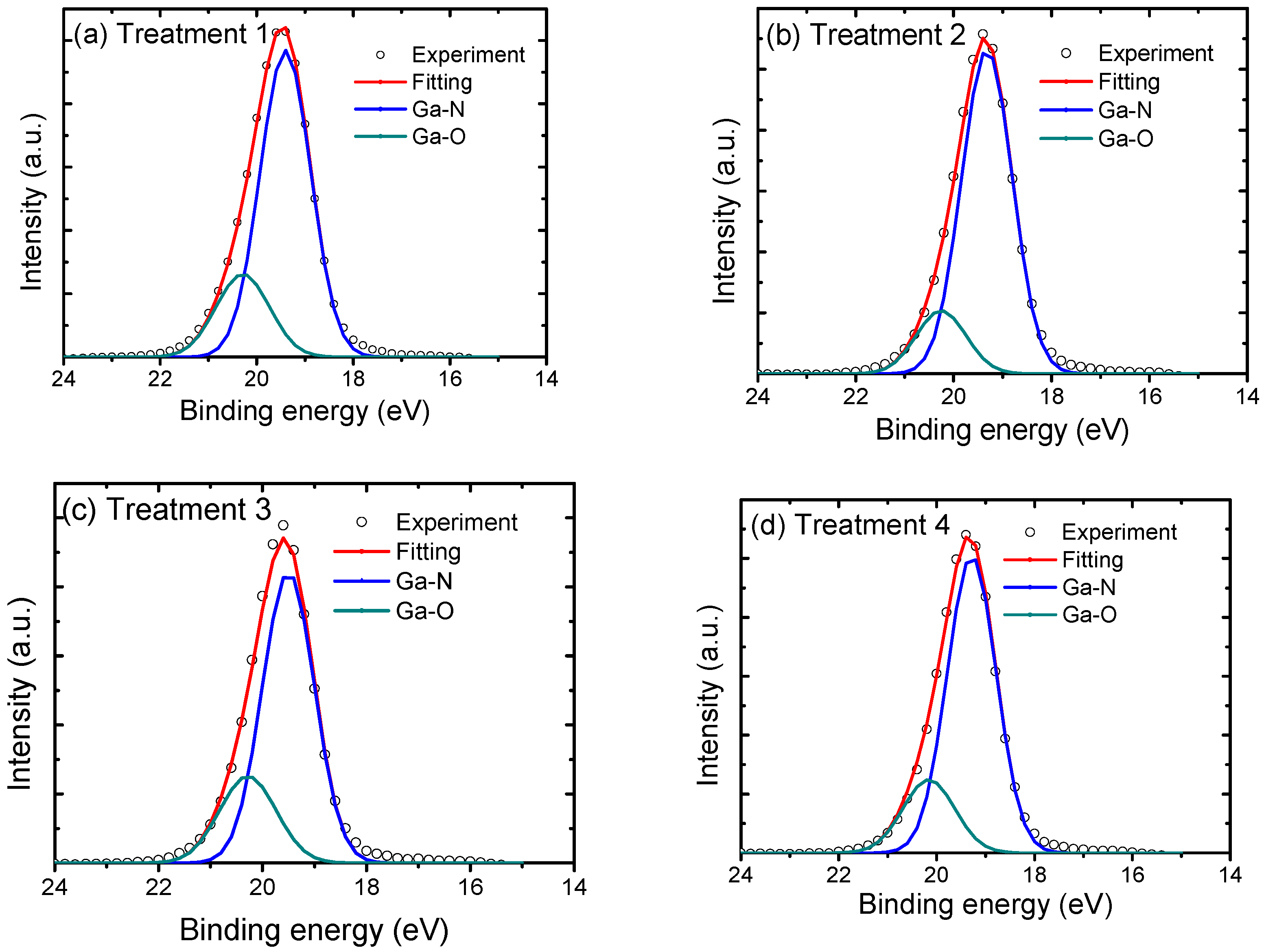
The
ρc is related to the surface barrier height of the GaN surface. The Ga–O to Ga–N ratio of the Ga3d peak was used to facilitate the analysis of the surface barrier height of GaN through various chemical treatments. XPS was used to study the surface composition on the GaN surface by using different chemical treatments.
Figure 3a–d shows the Ga3d core level of the XPS spectra. The Ga3d peaks of GaN obtained using treatments 1–4 appeared at 19.4, 19.4, 19.6, and 19.4 eV, respectively. A blue shift of approximately 0.2 eV was observed toward the high binding energy in a sample treated with treatment 3, compared with samples treated with the other treatments. This type of shift is assumed to have been caused by the loss of N at the surface or the creation of N vacancies, which would increase the n-type doping at the surface [
18]. In addition, the shift could have been caused by the BCl
3 plasma. Moreover, the Ga3d of XPS spectra photoelectrons can be separated into Ga–O and Ga–N components for various treatments. The main peak at a binding energy of 19.3 eV corresponded to the Ga–N bond, and the second peak at 20.3 eV corresponded to the Ga–O bond, thus confirming the presence of Ga
2O
3 as the native oxide layer on top of the GaN layer. The intensity and area of the Ga–O core level of the Ga3d peak after different treatments are functions of surface conditions. The Ga–O core level is reduced by a more complex chemical treatment association. The reduction of the Ga–O core level indicated that the Ga
2O
3 layer was effectively removed or reduced. Otherwise, the remaining Ga
2O
3 layer might affect the quality of the ohmic contact and thus increase the contact resistance between GaN and metal.
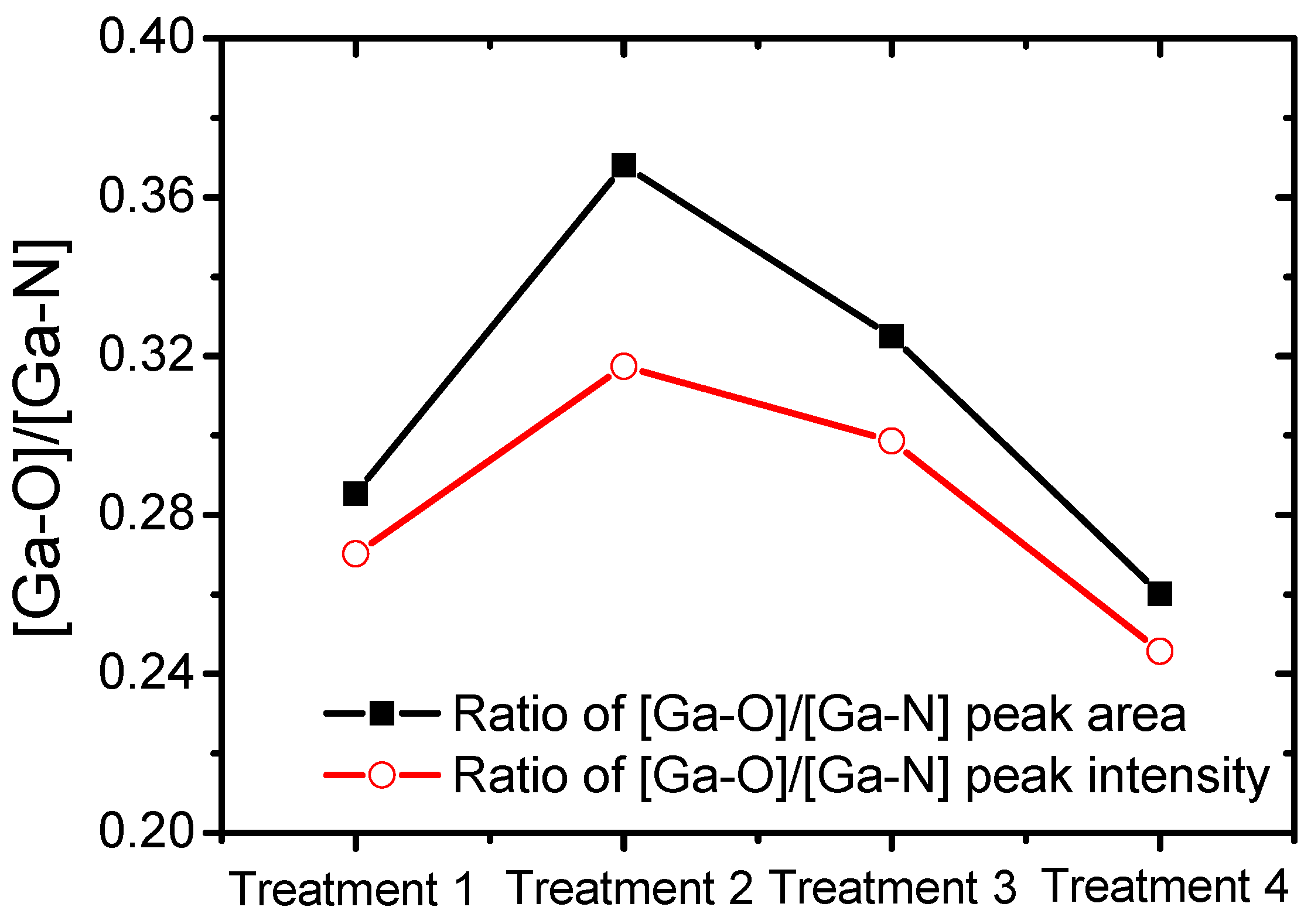
Figure 4 shows the integrated Ga–O core level levels, normalized using the Ga–N core level as a function of surface conditions to evaluate the residual native oxide layer on the GaN surface. The lowest Ga–O to Ga–N ratio of the Ga3d peak was obtained after treatment with treatment 4. Therefore, the
ρc of GaN contacted with Ti/Al/Ti/Au was the lowest for the sample treated with treatment 4. The area ratios of Ga–O to Ga–N obtained after different treatments are consistent with the contact characteristics of GaN with Ti/Al/Ti/Au (
Table 2). In addition, the peak ratio of Ga–O to Ga–N obtained using treatment 2 was the highest. This is because the Ga–O area of Ga3d obtained using treatment 2 was the highest, resulting in a high contact resistance. The Ga–O area was the highest because the fresh dangling bonds created by O
2 plasma and trap more O
2 existing in HCl:H
2O and HF:H
2O solutions. The [Ga–O]/[Ga–N] ratios decreased because of the reduction in the O concentration and/or increase in the N concentration at the GaN surface [
2]. In our study, samples treated with treatment 4 had the lowest [Ga–O]/[Ga–N] ratio. After O
2 plasma treatment, the residual GaO could be further etched by HF:H
2O, following oxidation by NH
4OH:H
2O and etched away by HCl:H
2O and HF:H
2O. The [Ga–O] decreased and [Ga–N] increased during GaO etching.
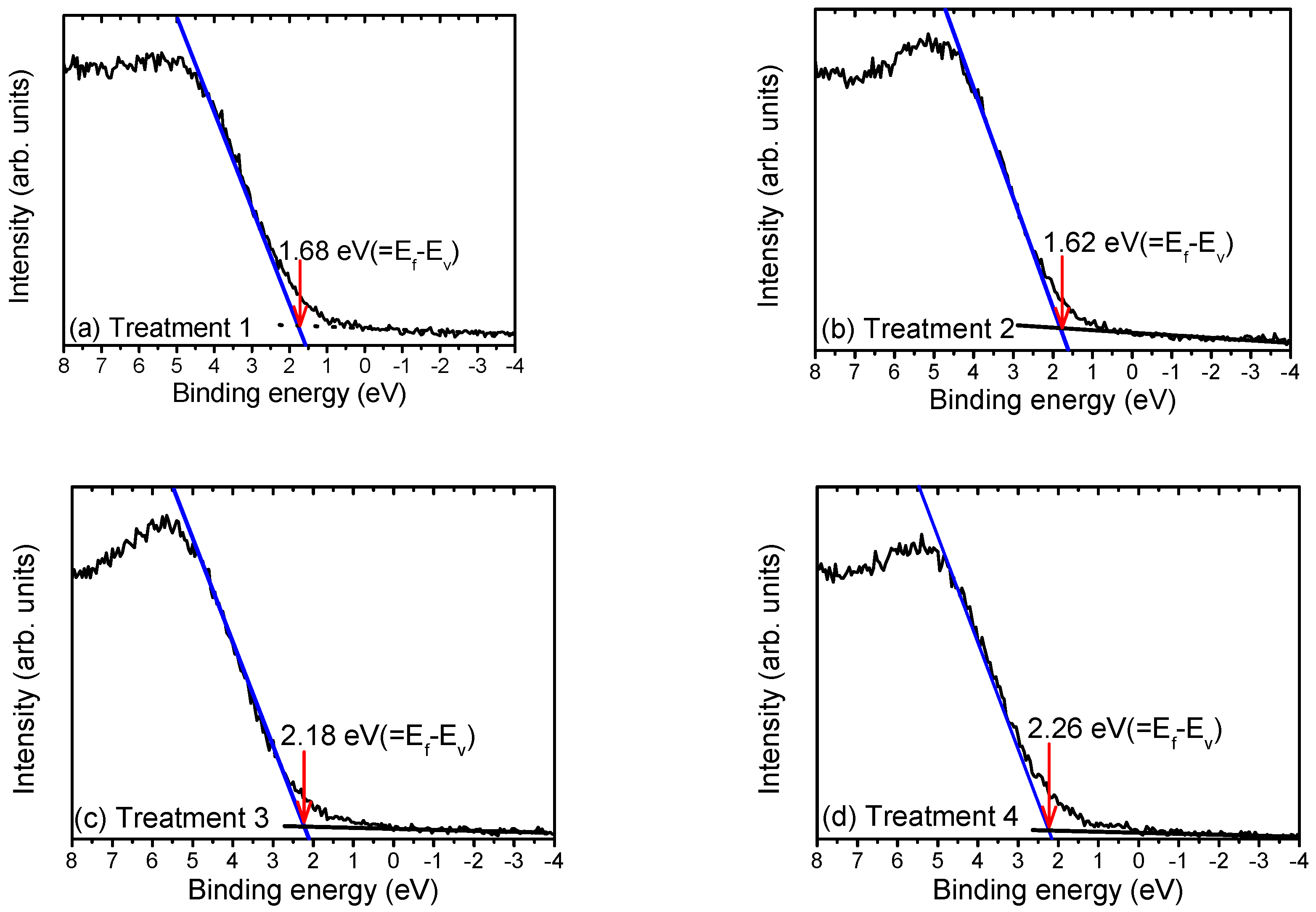
Figure 5 shows the XPS valence band spectra of GaN treated with various treatments. A binding energy of 0 eV on the horizontal axis corresponded to the energy position of the Fermi level (
Ef) at the surface. The energy position of the valence band maximum (VBM) was determined by linearly extrapolating the spectrum near the onset [
19] to calculate the surface barrier height of GaN. The surface barrier height (
ΦB) is defined as
Ec −
Ef, where
Ec is the energy position of the conduction band minimum. The VBM of GaN treated with different treatments was lower than the Fermi level by approximately 1.68–2.26 eV.
The surface treatment of GaN modifies the GaN surface condition, including surface barrier height, binding energy and surface quality, which will further change the GaN ohmic contact properties with Ti/Al/Ti/Au. The XPS valence band and XPS spectra were powerful enough to determine the surface barrier height of GaN after treatment. The high surface barrier height caused the poor ohmic contact. The surface barrier height of GaN after treatment with treatment 1–4 is shown in
Figure 6. The trend of the surface barrier height is consistent with that of the
ρc. A high
ρc indicates a high surface barrier height of GaN. The surface barrier height of the GaN surface after BCl
3 plasma treatment (in treatment 3) was lower than that of GaN after the treatment 1 and 2 treatments. The BCl
3 plasma increased the surface N vacancy of GaN, which acts as a donor-type density for electrons, thus increasing the surface doping concentration [
20]. The increase in the donor-type density of the GaN surface further improved the metallurgical process to reduce the surface barrier height of GaN during RTA. During RTA, Ti undergoes a metallurgical reaction with GaN, forming interfacial nitrides such as TiN. This can cause the GaN subsurface below the TiN to be heavily doped (n-type) [
21]. Therefore, the surface barrier height of GaN after treatment 3 was lower than that after treatments 1 and 2, and the surface barrier height of GaN after treatment 4 was the lowest. This result indicates that treatment 4 had the highest surface donor density, which contributed to a reduction in the ohmic contact resistance. A lower surface barrier height of GaN indicated a low contact resistance of GaN with Ti/Al/Ti/Au, thereby easily forming an ohmic contact for device applications.


