Article

Role of Hydrogen in Active Layer of Oxide-Semiconductor-Based Thin Film Transistors

Intelligent Devices & Systems Research Group, Institute of Convergence, DGIST, Daegu 42988, Korea
*
Author to whom correspondence should be addressed.
Crystals 2019, 9(2), 75; https://doi.org/10.3390/cryst9020075
Submission received: 26 December 2018 / Revised: 24 January 2019 / Accepted: 30 January 2019 / Published: 31 January 2019
(This article belongs to the Special Issue Thin Film Transistor)

Abstract

:
Hydrogen in oxide systems plays a very important role in determining the major physical characteristics of such systems. In this study, we investigated the effect of hydrogen in oxide host systems for various oxygen environments that acted as amorphous oxide semiconductors. The oxygen environment in the sample was controlled by the oxygen gas partial pressure in the radio-frequency-sputtering process. It was confirmed that the hydrogen introduced by the passivation layer not only acted as a “killer” of oxygen deficiencies but also as the “creator” of the defects depending on the density of oxide states. Even if hydrogen is not injected, its role can change owing to unintentionally injected hydrogen, which leads to conflicting results. We discuss herein the correlation with hydrogen in the oxide semiconductor with excess or lack of oxygen through device simulation and elemental analysis.

1. Introduction

Amorphous oxide semiconductors have been extensively investigated for application in transparent electronics, backplanes of large-area active-organic light-emitting diode displays, and liquid crystal displays [1]. Among devices made using various oxide semiconductor materials, amorphous indium–gallium–zinc–oxide (a-IGZO) thin film transistors (TFTs) exhibit a wide range of electron densities (Ne) ranging [2] from 1011 to 1019 cm−3. Oxide semiconductors with wide band gaps, along with these high electron densities, are considered to be a promising alternative to amorphous silicon TFTs because they can provide high mobility and low leakage currents.
However, a-IGZO TFTs still present problems in the form of various defects between the metal and the oxygen, such as deficiencies (similar to vacancies in a crystal system) and interstitial defects, which they strongly affect the electrical properties of the devices and their reliability in practical applications [3,4,5,6]. In addition to such intrinsic defects, it is well known that hydrogen as an impurity can also affect the electrical properties of a-IGZO TFTs. Hydrogen, which results in high conductivity due to form the donor level above conduction band, can be found in various forms in crystalline oxide semiconductors [7,8]. It can be present as interstitial hydrogen (Hi), located at bond-centered or antibonding sites owing to O-H bonds [9]. A second type can be trapped at oxygen deficiencies (Ho) [10]. The final kind is unbound hydrogen, or the interstitial H2 [11]. Hydrogen impurity present in high densities of 1020–1021 cm−3 is always found in a-IGZO films [2]. When it forms bonds with oxygen and generates negatively charged hydroxide anions, hydrogen becomes a shallow donor, generating free carriers in the oxide semiconductors. On the other hand, hydrogen can deactivate defects in a-IGZO due to compensation by excess oxygen, which manifests as defect passivation [12]. Many studies have been conducted in an effort to reveal the effects of hydrogen on defects of a-IGZO and have involved techniques such as hydrogen plasma treatment [13], annealing temperature control in hydrogen ambient [14], and hydrogen injection through buffer layers [15]. Oh et al. investigated the hydrogenation of a-IGZO films under high-pressure hydrogen annealing at different temperatures [16]. A very high carrier density (Ne) of 1.63 × 1019 cm−3 was observed as a result, which is 105 times higher than that of as-grown films. Nguyen et al. reported the influence of hydrogen arising from silane (SiH4) in the passivation layer on the device properties [17]. It was clearly observed that the Vth shifted negatively and the leakage current seemed to increase on increasing the silane concentration. This hydrogen incorporation into a-IGZO induced excess carriers in channels, making the system a better conductor. Han et al. studied the effect of a multi-layered buffer on the electrical properties of a-IGZO TFTs [18]. When the amount of diffused hydrogen in the a-IGZO layer was under a critical value, electron trapping at the a-IGZO/insulator interface was effectively suppressed by deactivation of defect states in the a-IGZO layer. Conversely, hydrogen diffusion from the hydrogen-rich layer caused a conducting channel. Other roles were assumed for hydrogen in a-IGZO TFTs and difficulty in achieving precise control of hydrogen during the fabrication of TFTs make this issue more difficult to resolve [18].
So far, studies in this area have been mainly conducted focusing on hydrogen, regardless of the oxide semiconductor host system. In this work, we studied the effect of hydrogen in host systems with various oxygen environments in amorphous oxide semiconductors. We found that the hydrogen introduced by the passivation layer not only acts as the “killer” of oxygen deficiencies but also as the “creator” of defect levels depending on the density of oxide states. Its role strongly depends on the host oxide semiconductor system, especially on the oxygen environments between the metal cations. Herein, we have discussed the role of hydrogen in oxygen-excess systems as well as oxygen-deficient systems, and have confirmed our results through device simulation and elemental analysis.

2. Materials and Methods
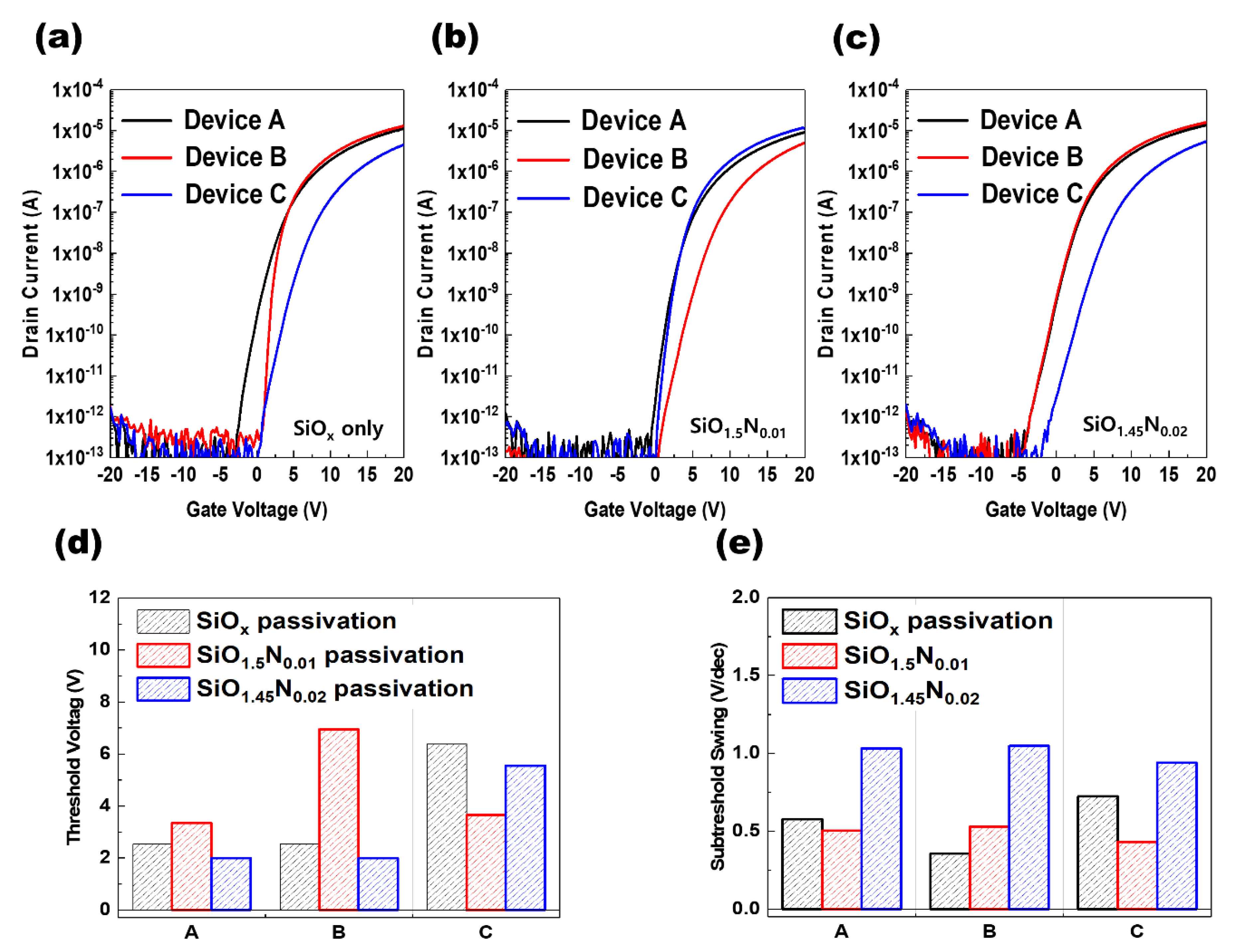
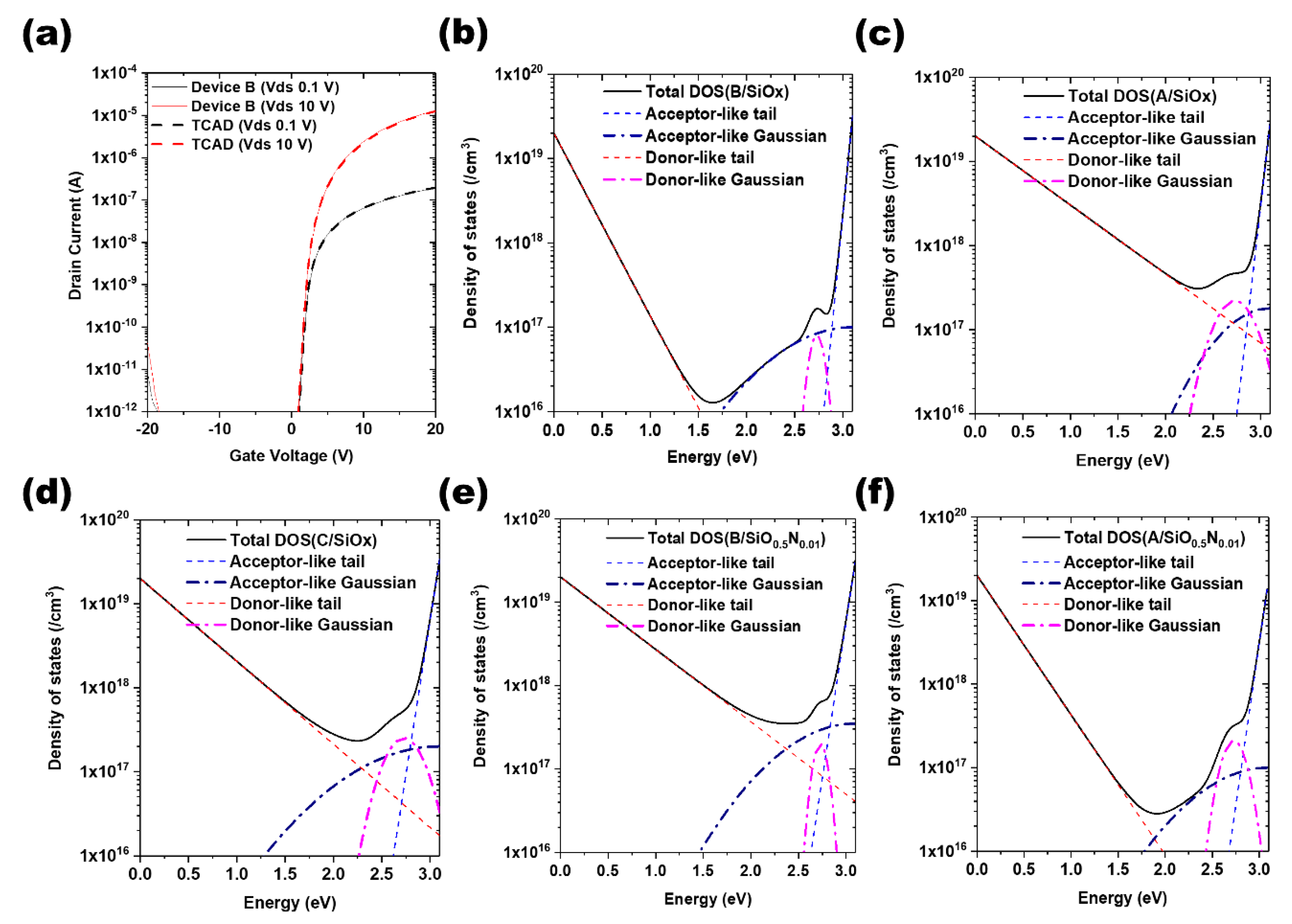
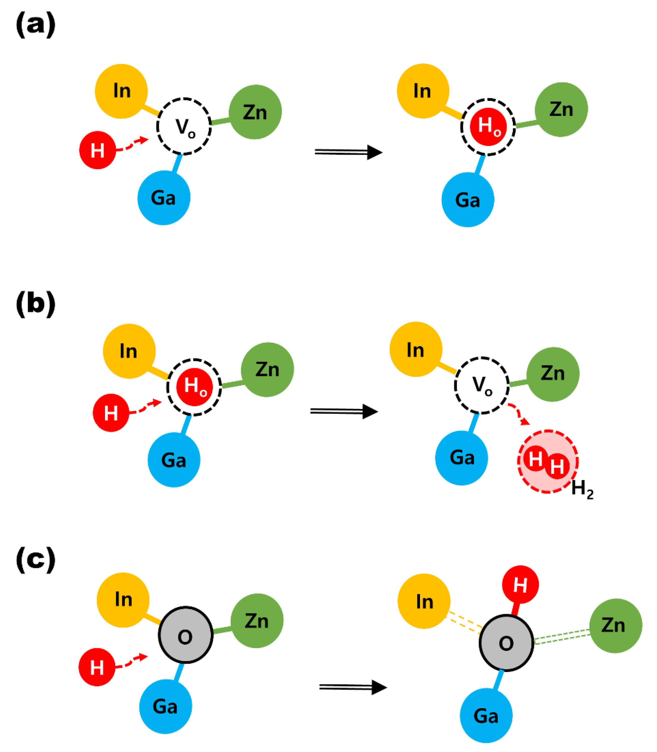
The TFTs with a bottom-gate inverted staggered structure, as shown in Figure 1a, were fabricated on a silicon wafer substrate. A Au (100 nm) gate electrode was deposited by the direct current (DC) magnetron sputtering method. Dual layers of a-SiNx (50 nm)/SiOx (150 nm) were subsequently deposited as a gate insulator by plasma-enhanced chemical vapor deposition (PECVD, KCT, Inc., Gyeonggi-do, Korea) at 350 °C. A 40-nm-thick a-IGZO active layer (In:Ga:Zn = 1:1:1 by mol%) was deposited by radio frequency (RF) magnetron sputtering (4 inch target, distance of 120 mm between the source and the substrate, Korea Vacuum Tech, Inc., Gyeonggi-do, Korea) at 100 °C using a gas mixture of Ar and O2 and an input power of 200 W (5 mTorr). A Au S/D layer (100 nm) was deposited and patterned by photolithography (W/L = 10 µm/10 µm) followed by lift-off. The gate-via was formed by a reactive ion dry etching process. The single passivation layer (without SiOxNy) of SiOx (200 nm) and dual passivation layers of SiOx (100 nm)/ SiOxNy (100 nm) were subsequently deposited under the same conditions with the gate insulator layers. Finally, the deposited layers were annealed at 350 °C for 1 h under vacuum. SiOxNy was considered to be a likely source of hydrogen and its value was controlled by the ratio of the precursor materials, the nitrous oxide (N2O) and ammonia (NH3), at values of SiOx, SiO1.5N0.01, and SiO1.45N0.02 (The ratio of oxygen and nitrogen was estimated by x-ray photoelectron spectroscopy (XPS)). Samples were prepared using RF-sputtering under three different oxygen partial pressures. Detailed conditions of which has been provided in Table 1. A Keithley 2636B source meter (Keithley Instrument, Inc., OH, USA) was used to determine the electrical characteristics. The surface properties and bonding character were investigated by XPS (Thermo Scientific, Inc., MA, USA) and time-of-flight secondary ion mass spectroscopy (TOF-SIMS, Ion-tof, Inc., Münster, Germany) was utilized to measure and analyze the hydrogen concentration in the active layer. The device was simulated using technology computer aided design (TCAD, Silvaco, Inc., CA, USA, 2018) to understand the electron transport properties, using Silvaco’s 2D ATLAS simulator package (Silvaco Inc., CA, USA, 2018) [19,20].

3. Results

To identify the effect of hydrogen for different host system environments in the active layer, hydrogen was introduced by various SiOxNy passivation layer conditions in the a-IGZO. The hydrogen densities depending on the passivation in a-IGZO are shown in Figure 1b. The density of hydrogen was estimated to be >1020 atom/cm−3 in the entire samples and the density increased with increasing nitrogen concentration in the passivation layer. Since the nitrogen precursor of the SiOxNy layer was NH3 in the PECVD process, the hydrogen density strongly depended on the nitrogen concentration [17]. Figure 2 compares the transfer characteristics (Vds = 10 V) of a-IGZO TFTs influenced by hydrogen via the passivation layer depending on the oxygen partial pressure, “Device A, Device B, and Device C”.
An increasing threshold voltage (the linear extraction method in the saturation region) was observed as the oxygen partial pressure increased, as seen in Figure 2a. Increase in the oxygen partial pressure from 0.7 to 1 sccm gave rise to a decrease in the subthreshold swing (voltage with an order current at the maximum I-V gradient; ln 10 dVG/d(ln ID) ) value from 0.58 to 0.36 V/dec. However, the partial pressure continuously increasing to 5 sccm caused an increase in the subthreshold swing value. It seemed that the oxygen partial pressure alone was able to not only control the oxygen deficiency in the oxide semiconductor devices but also create an impurity level due to the excess oxygen. Injection of excessive oxygen causes an increase in subthreshold swing due to an increasing number of defect states and the positive shift in the threshold voltage, as shown in Figure 2a. The electrical properties changing as a function of the additional SiOxNy layer is shown in Figure 2b,c. At a low oxygen partial pressure (Device A), the threshold voltage, shown in Figure 2a, increased to 3.34 V but the subthreshold swing value decreased to 0.50 V/dec when the second passivation SiO1.5N0.01 layer was deposited as shown in Figure 2d,e. On the other hand, at a high oxygen partial pressure (Device C), we observed decreasing threshold voltage and subthreshold swing values. It was proposed that two different phenomena were brought about by the additional hydrogen in the two different host systems. The first was a passivation effect, which is a well-known phenomenon that reduces the oxygen deficiency states via hydrogen substitution in oxygen-deficient sites. In the case of the excess-oxygen sample, it seemed that the hydrogen reduced the defect states that were below the conduction band minimum and were formed by the excess oxygen in the oxide semiconductor. Above all, it was interesting to observe that the additional hydrogen could form defect states. The sample showing good electrical transfer characteristics, Device B in Figure 2a, underwent drastic changes in the electric characteristics through hydrogen injection via added passivation by SiO1.5N0.01 as shown in Figure 2b. Figure 2c shows the electrical transfer curves of the sample with a SiO1.45N0.02 passivation layer and a high subthreshold swing value of around 1.0 V/dec. This suggested that the continued increasing amount of hydrogen gave rise dominant formation of defect states.
In order to understand the defect generation by hydrogen through the passivation layer, a 2-dimensional numerical TCAD simulation was used to simulate the device characteristics. In Figure 3a, both black (Vds 0.1 V) and red (Vds 10 V) solid lines show the measured I–V transfer curves of “Device B” with SiOx passivation. Both dashed lines indicate the simulated I–V transfer curves and these matched well with the measured I–V data. Figure 3b shows the initial band gap states along with the tailing and sub-gap states of the a-IGZO. The peak density of the donor-like tail state near the valence band and the donor-like Gaussian state below the conduction band were calculated to be 2.0 × 1019 cm−3eV−1 (width of the state: 0.2 eV) and 3.2 × 1019 cm−3eV−1 (width of the state: 0.037 eV), respectively. A broad acceptor-like Gaussian state, 0.9 eV, and a narrow donor-like Gaussian state, 0.1 eV, were confirmed on the band gap. A decreasing oxygen partial pressure reduced the acceptor-like Gaussian broadening but increased the width of the donor-like Gaussian state as well as that of the donor-like tailing state, as shown in Figure 3c. In the excess-oxygen case, broadening of the acceptor-like Gaussian state increased significantly from 0.61 eV to 1.05 eV, as shown in Figure 3d. Figure 3e,f show the simulated density of states for the effects of the hydrogen. The increasing hydrogen concentration in the active layer owing to the passivation layer (SiO0.5N0.01) increased the defect states, especially the donor-like tailing states and acceptor-like Gaussian states. Figure 3e shows the density of state in Device B with SiO0.5N0.01 passivation, which was comparable to that in Device B with SiOx passivation, as shown in Figure 3b. In addition, the hydrogen introduced in the oxygen-deficient sample, Device A with SiOx passivation, reduced the defect energy levels. In this case, the width of the donor-like tailing state and donor-like Gaussian states decreased drastically and the band edge below the conduction band minimum was relatively sharp, as shown in Figure 3f.
Hydrogen is a typical element that is unintentionally injected into sample layers. Because this hydrogen has a significant effect on the device properties, hydrogen can be used in various ways in its semiconductor process. Hydrogen in InGaZnO, a major oxide semiconductor, is able to replace [21] oxygen deficiency sites, and the defect states arising due to a lack of oxygen are removed as shown in Figure 4a. Due to these passivation effects of the oxygen deficiency state, many studies have used hydrogenation processes to secure initial electrical characteristics and long-time reliability. However, this hydrogen injection cannot only play a positive role. The abovementioned results depicted in Figure 2 and Figure 3 confirmed that excessive injection of hydrogen can cause various defect states. It was confirmed by 2-dimensional TCAD device simulation that excessive hydrogen can give rise to donor-like tailing states and acceptor-like Gaussian defect states. Figure 4b,c are schematics of the possible impurities of hydrogen injection. Injection of excess hydrogen can lead to its conversion to the molecular H2 state [11] (Figure 4b), and the reduction reaction via hydrogenation can also weaken the binding energy of oxygen and weakly bound In or Zn, as shown in Figure 4c.

4. Conclusions

In this paper, we reported the effects of hydrogen on the host system for various oxygen environments in amorphous oxide semiconductors. We employed a-IGZO as an oxide semiconductor for our investigation. Hydrogen injection was adjusted by changing the passivation layer conditions and increased hydrogen concentration was confirmed using SIMS. Electrical measurements and simulations showed that hydrogen played a role in eliminating oxygen deficiencies, which is the biggest issue in oxide semiconductors, and excess injection of hydrogen produced additional structural defects in the host system. On injecting hydrogen into oxide semiconductors, in particular, hydrogen may play different roles as the species that reduces defect states depending on the oxygen environments of the host system or the one that increases defect states.

Author Contributions

H.-J.L. designed the experimental concept and wrote the main text of the manuscript. H.Y.N. fabricated the device. J.K., J.-S.K. and M.-J.L. contributed to the circuit design and the overall understanding of the device physics. All authors reviewed the manuscript.

Funding

This research was supported in part by the DGIST R&D Program of the Ministry of Science, ICT, and Future planning (18-NT-01) and in part by the Basic Science Research Program through the National Research Foundation of Korea (NRF) under Grant NRF-2018R1D1A1B07041075.

Conflicts of Interest

The authors declare no conflict of interest.

References

  1. Nomura, K.; Ohta, H.; Takagi, A.; Kamiya, T.; Hirano, M.; Hosono, H. Room-temperature fabrication of transparent flexible thin-film transistors using amorphous oxide semiconductors. Nature 2004, 432, 488–492. [Google Scholar] [CrossRef] [PubMed]
  2. Tang, H.; Kishida, Y.; Ide, K.; Toda, Y.; Hiramatsu, H.; Matsuishi, S.; Ueda, S.; Ohashi, N.; Kumomi, H.; Hosono, H.; et al. Multiple Roles of Hydrogen Treatments in Amorphous In–Ga–Zn–O Films. ECS J. Solid State Sci. Technol. 2017, 6, P365–P372. [Google Scholar] [CrossRef]
  3. Kamiya, T.; Hosono, H. Material characteristics and applications of transparent amorphous oxide semiconductors. NPG Asia Mater. 2010, 2, 15–22. [Google Scholar] [CrossRef] [Green Version]
  4. Xiao, X.; Deng, W.; Chi, S.; Shao, Y.; He, X.; Wang, L.; Zhang, S. Effect of O2 Flow Rate During Channel Layer Deposition on Negative Gate Bias Stress-Induced Vth Shift of a-IGZO TFTs. IEEE Trans. Electron Devices 2013, 60, 4159–4164. [Google Scholar] [CrossRef]
  5. Lee, H.-J.; Cho, S.H.; Abe, K.; Lee, M.-J.; Jung, M. Impact of transient currents caused by alternating drain stress in oxide semiconductors. Sci. Rep. 2017, 7, 9782–9790. [Google Scholar] [CrossRef] [PubMed]
  6. Lee, H.-J.; Abe, K.; Cho, S.H.; Kim, J.-S.; Bang, S.; Lee, M.-J. Drain-Induced Barrier Lowering in Oxide Semiconductor Thin-Film Transistors with Asymmetrical Local Density of States. IEEE J. Electron Devices Soc. 2018, 6, 830–834. [Google Scholar] [CrossRef]
  7. Nomura, K.; Kamiya, T.; Hosono, H. Effects of Diffusion of Hydrogen and Oxygen on Electrical Properties of Amorphous Oxide Semiconductor, In-Ga-Zn-O. ECS J. Solid State Sci. Technol. 2013, 2, P5–P8. [Google Scholar] [CrossRef]
  8. Bang, J.; Chang, K.J. Diffusion and thermal stability of hydrogen in ZnO. Appl. Phys. Lett. 2008, 92, 132109. [Google Scholar] [CrossRef]
  9. Van de Walle, C.G. Hydrogen as a Cause of Doping in Zinc Oxide. Phys. Rev. Lett. 2000, 85, 1012–1015. [Google Scholar] [CrossRef] [PubMed] [Green Version]
  10. Lavrov, E.V.; Herklotz, F.; Weber, J. Identification of two hydrogen donors in ZnO. Phys. Rev. B 2009, 79, 165210. [Google Scholar] [CrossRef]
  11. Lavrov, E.V.; Herklotz, F.; Weber, J. Identification of Hydrogen Molecules in ZnO. Phys. Rev. Lett. 2009, 102, 185502. [Google Scholar] [CrossRef] [PubMed]
  12. Nam, Y.; Kim, H.-O.; Cho, S.H.; Park, S.-H. Effect of hydrogen diffusion in an In–Ga–Zn–O thin film transistor with an aluminum oxide gate insulator on its electrical properties. RSC Adv. 2018, 8, 5622–5628. [Google Scholar] [CrossRef] [Green Version]
  13. Kim, J.; Bang, S.; Lee, S.; Shin, S. A study on H2 plasma treatment effect on a-IGZO thin film transistor. J. Mater. Res. 2012, 27, 2318–2325. [Google Scholar] [CrossRef]
  14. Abliz, A.; Gao, Q.; Wan, D.; Liu, X.; Xu, L.; Liu, C.; Li, X.; Chen, H.; Guo, T.; Li, J.; et al. Effects of Nitrogen and Hydrogen Codoping on the Electrical Performance and Reliability of InGaZnO Thin-Film Transistors. ACS Appl. Mater. Interfaces 2017, 9, 10798–10804. [Google Scholar] [CrossRef] [PubMed]
  15. Tari, A.; Wong, W.S. Effect of dual-dielectric hydrogen-diffusion barrier layers on the performance of low-temperature processed transparent InGaZnO thin-film transistors. Appl. Phys. Lett. 2018, 112, 073506. [Google Scholar] [CrossRef]
  16. Oh, S.I.; Choi, G.; Hwang, H.; Lu, W.; Jang, J.-H. Hydrogenated IGZO Thin-Film Transistors Using High-Pressure Hydrogen Annealing. IEEE Trans. Electron Devices 2013, 60, 2537–2541. [Google Scholar] [CrossRef]
  17. Nguyen, T.T.T.; Aventurier, B.; Terlier, T.; Barnes, J.; Templier, F. Impact of Passivation Conditions on Characteristics of Bottom-Gate IGZO Thin-Film Transistors. J. Disp. Technol. 2015, 11, 554–558. [Google Scholar] [CrossRef]
  18. Han, K.-L.; Ok, K.-C.; Cho, H.-S.; Oh, S.; Park, J.-S. Effect of hydrogen on the device performance and stability characteristics of amorphous InGaZnO thin-film transistors with a SiO2/SiNx/SiO2 buffer. Appl. Phys. Lett. 2017, 111, 063502. [Google Scholar] [CrossRef]
  19. ATLAS Device Simulation Software User’s Manual; Silvaco International: Santa Clara, CA, USA, 2015.
  20. Lee, H.-J.; Abe, K.; Kim, J.S.; Lee, M.-J. Electron-blocking by the potential barrier originated from the asymmetrical local density of state in the oxide semiconductor. Sci. Rep. 2017, 7, 17963–17970. [Google Scholar] [CrossRef] [PubMed]
  21. Janotti, A.; Van de Walle, C.G. Hydrogen multicentre bonds. Nat. Mater. 2007, 6, 44–47. [Google Scholar] [CrossRef] [PubMed]
Figure 1. (a) Cross-sectional schematic of the bottom-gate inverted staggered structure of a-InGaZnO TFT. (b) TOF-SIMS depth profile of hydrogen atoms in a-IGZO of device B.
Crystals 09 00075 g001
Figure 2. Electric transfer curves of a-IGZO TFTs with passivation by (a) SiOx, (b) SiO1.5N0.01, and (c) SiO1.45N0.02. Summary of the (d) threshold voltage and (e) subthreshold swing.
Crystals 09 00075 g002
Figure 3. (a) I–V transfer curves for Device B with SiOx passivation, measured and simulated. TCAD simulated density of states for (b) Device B, with SiOx; (c) Device A, with SiOx; (d) Device C, with SiOx; (e) Device B, with SiO0.5N0.01; and (f) Device A, with SiO0.5N0.01. The variation of the oxygen partial pressure give rise to noticeable change the “Donor-like Gaussian” state as well as “Donor-like tail” state. The center of the “Donor-like Gaussian” state is around 2.73 eV.
Crystals 09 00075 g003
Figure 4. Schematic structure for the hydrogen and oxygen migration process for cases involving (a) trapped hydrogen in oxygen-deficient state, (b) unbound hydrogen, and (c) weak bonding of In and Zn with oxygen bound to hydrogen.
Crystals 09 00075 g004
Table 1. Ar/O2 partial pressure conditions in the radio frequency (RF) sputtering.
DeviceAr
(sccm)
O2
(sccm)
Device A500.7
Device B501.0
Device C505.0

