1. Introduction
High-powered solid-state laser devices are capable of generating extreme physical conditions, such as a strong electric field, a strong magnetic field, and a high voltage intensity in the laboratory, which not only support frontier scientific research, such as high-energy-density physics, but they also play a significant role in the national economy, national defense, and in military fields. With the increasing energy output and hit times, the problem of laser damage to its optical components is gradually become a formidable challenge for the laser device. For instance, HfO2/SiO2 thin film is one of the most easily damaged components in laser devices. The actual laser threshold is always far below the theoretical threshold and that limits the output capability of laser devices.
To improve the laser output capability, extensive research has been carried out all over the world on the damage mechanism of thin films [
1]. It is generally understood that the absorption of laser light by various types of defects in thin films is an important cause of damage [
2,
3,
4,
5]. Wu et al. and Bloembergen both found that dielectric film defects, such as nodules, have an additional absorption of laser light that lowers the overall damage threshold of the film [
6,
7]. Cheng et al. proposed that defects act as absorbers, and a large amount of thermal deposition around them eventually destroys the coating [
8,
9,
10]. Smalakys et al.’s study found that delamination of the coating occurred when the density of the subcritical damage reached a critical point, followed by the rapid growth of damage pits [
11]. Zhao et al. and Sozet et al.’s studies showed that delamination could be due to mechanical failure caused by a high density of subcritical damage [
12,
13] or due to scattering of subcritical damage [
14] caused by high-intensity areas. Smalakys found that the same optical component, due to different means of preparation, processing, etc., can also have a large difference in the damage threshold of the component due to the presence of various types of defects during the deposition process, and even high-quality optical films with optimal post-deposition processing can show different damage results [
15]. Due to the input geometry, the craters on the film surface are formed by plastic deformation from the recoil pressure on the contaminated particles [
16]. The absorption of optical films may be the intrinsic absorption of the film material or additional absorption introduced during preparation, along with nonlinear absorption, such as multiphoton ionization and electron avalanche breakdown [
17]. A large number of studies have shown that the main reason for the irradiation damage of optical films is thermal melting damage and mechanical damage caused by laser energy absorbed by nano-scale defects on the film surface and interface [
18,
19,
20,
21,
22].
Although the influence of the presence of various defects on the dielectric film damage performance has been largely determined, the subsequent change in damage growth after damage generation, the difference in performance before and after irradiation of the optical components have been less studied, and it is important to predict the damage growth behavior and the difference in performance before and after component damage.
In this paper, we choose HfO2/SIO2 multilayer dielectric film samples as the research object, and subject them to surface morphology tests, sample performance tests, damage threshold experiments, and damage area growth experiments to investigate the damage properties of the samples, investigate the influence of the initial damage morphology on the subsequent damage growth and the influencing factors. The reason for the difference in the growth of the two types of damage was determined by the surface morphology test, which deepened the understanding of the research on the growth of dielectric film damage.
2. Experiment
2.1. Sample Introduction
The experimental samples were coated with alternating HfO
2/SiO
2 multilayer high reflectivity dielectric films deposited by electron beam evaporation, and small-sized samples (50 × 50 × 5 mm
3) were selected. The substrate of the samples is K9 glass, and the refractive indices of the film materials at different wavelengths are shown in
Table 1 and
Table 2.
Reflectance testing of the samples was carried out on a UV7600 double-beam UV–visible spectrophotometer from Lengguang technology, and the reflection spectrum of the sample was obtained, as shown in
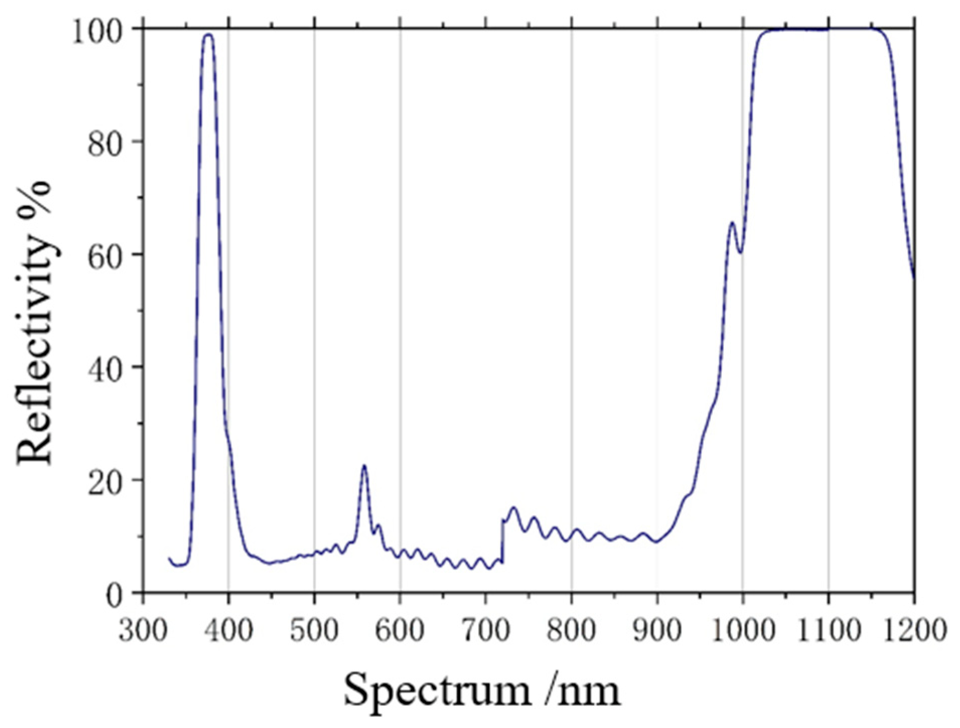
Figure 1. The reflectance of the sample can reach nearly 100% at the wavelength of 375 nm and 1064 nm. The reflectivity is 98.5% at 375 nm and 99.6% at 1064 nm. In the wavelength range from 400 nm to 900 nm, the reflectance is significantly reduced to less than 30%, which meets the requirements for engineering use. Using a DEXUN SPMI-600D Profiler, the test obtained a film roughness of 2.1 nm.
2.2. Damage Test Device and Test Method
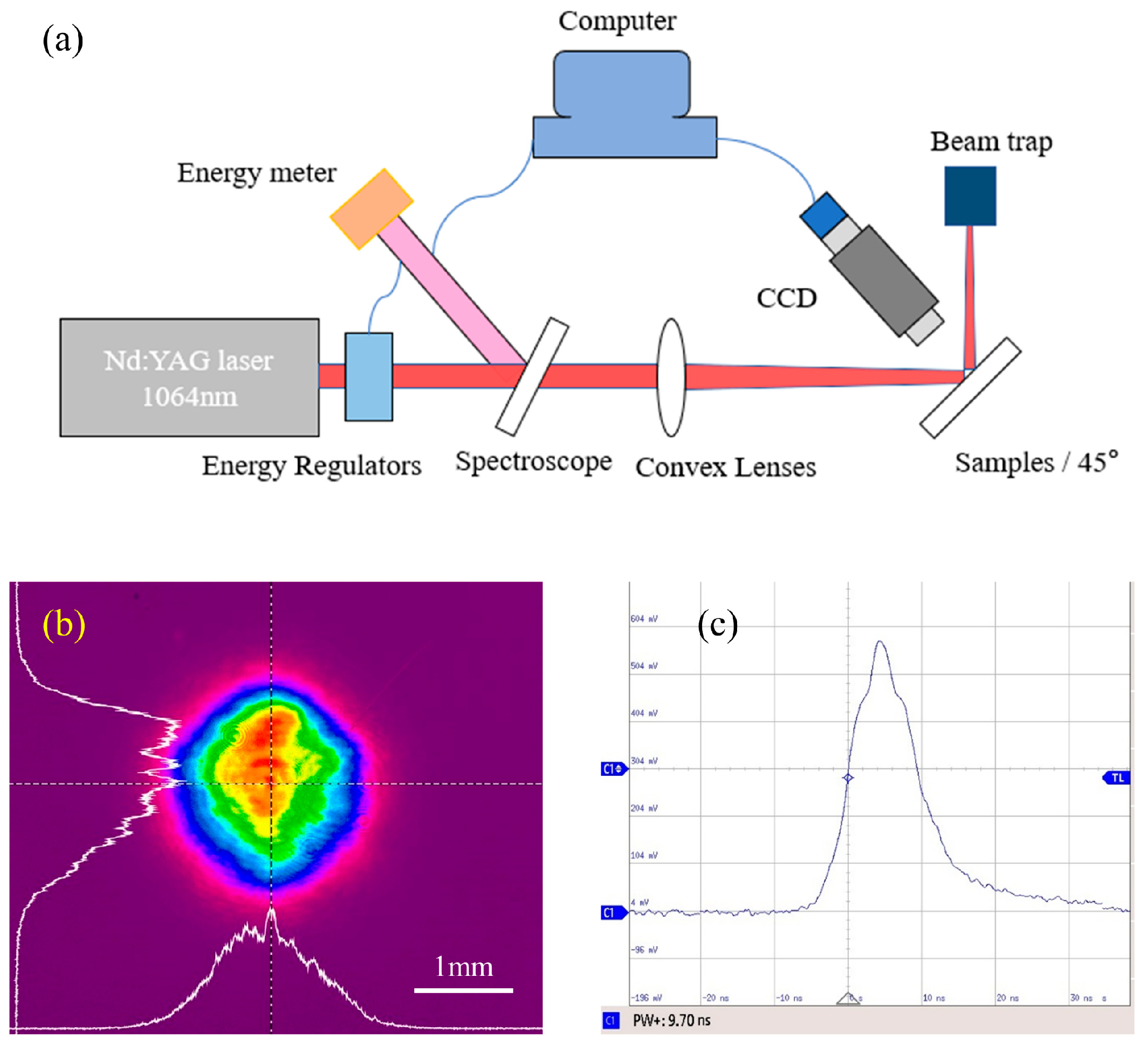
The multi-longitudinal mode Nd: YAG laser was used for the experiments. The schematic diagram of the laser damage testing device is shown in
Figure 2a, with an output wavelength of 1064 nm and a pulse width of 9 ns (
Figure 2c). The area of the light spot is 3.6 mm
2, the quality of light is favorable, both transverse and longitudinal light intensities are relatively uniform, and the maximum energy output accuracy of the laser is 100 mJ. The microscopic imaging system was used to perform the online monitoring of the damage and consisted of a microscope and CCD for the online observation by computer with a resolution of ~6 μm. The dielectric film sample was placed at an angle of 45° to the optical path. The role of the beam splitter is to perform the fixed beam splitting of the main laser beam, and after beam splitting, the low-energy beam enters the beam diagnostic device, which gives the beam information, such as spatial distribution of the laser pulses, time distribution, and beam splitting energy. The outgoing laser is focused on the sample optical surface by the optical path, the sample position spot area is 1.07 mm
2, as in
Figure 2b, and the spot tuning system is 1.8. The 1-on-1, R-on-1, and damage area growth experiments are performed on the sample using this device, and the damage of the sample is recorded by the microscopic imaging system during the experiments.
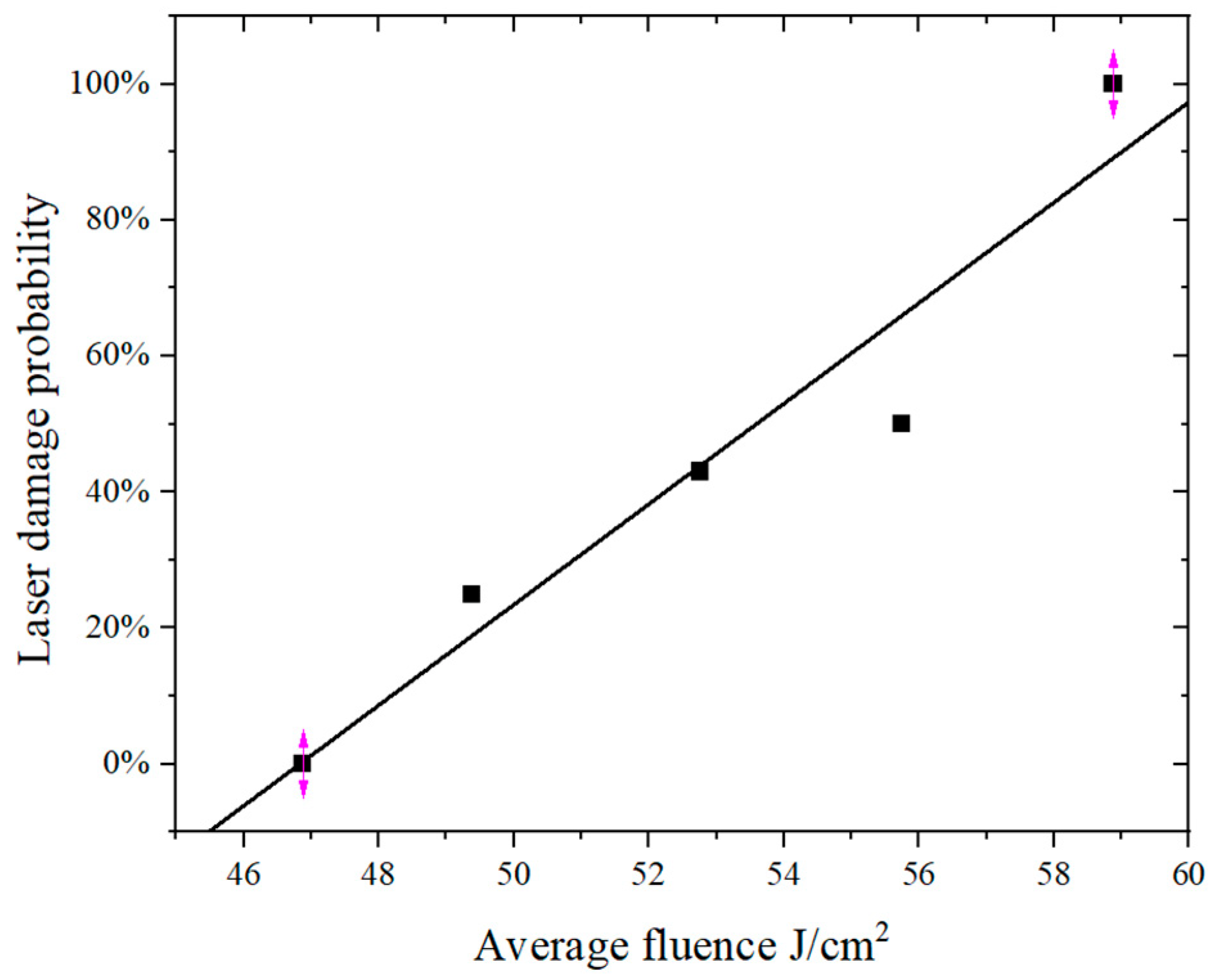
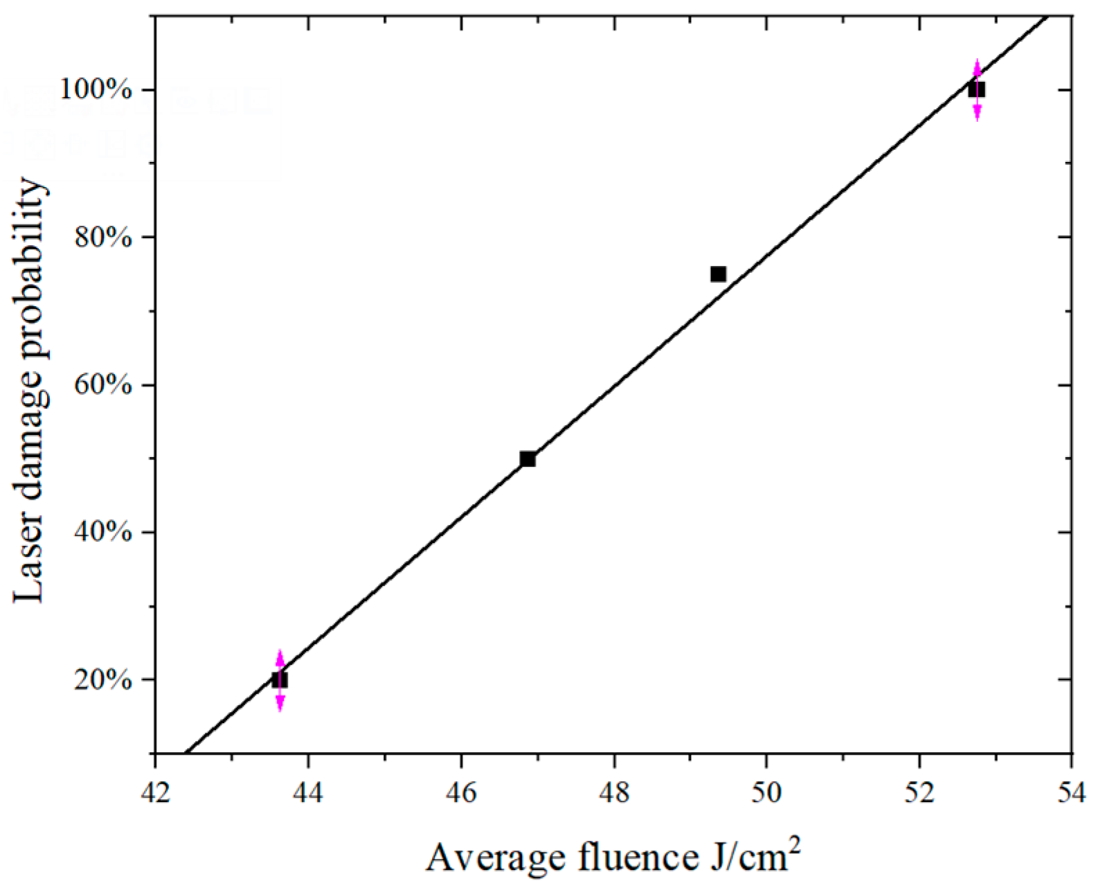
The initial damage threshold and subsequent damage growth threshold of the samples were measured using the R-on-1, as well as the 1-on-1 test methods. The R-on-1 experimental method is for the same location of the sample, hit once with a flux far below the damage threshold, increasing a small amount of flux step by step, and once at each flux until the damage occurs. It records the flux at the time of damage and tests 15 points per sample, respectively, to calculate the probability of damage at each flux when damage occurs.
The 1-on-1 experimental method hits each sample once at the same flux at different locations. It records the damage probability at that flux, and varies the flux until 0 damage probability and 100% damage probability are obtained. It tests 15 points for each flux. Both experimental methods were used to derive the damage probability curves at different fluxes, and the damage threshold for the experiment was obtained after fitting.
3. Results and Analysis
3.1. Initial Damage
During the damage performance testing of the samples, we documented all changes in the damage patterns, and only two different types of damage patterns were observed in the experiment. Type 1 damage manifested as film layer color and height changes and type 2 damage manifested as damage pit film layer peeling or melt-like damage. The initial threshold values of the two types of damage are different, and the subsequent impact on the damage performance of the film layer is also different.
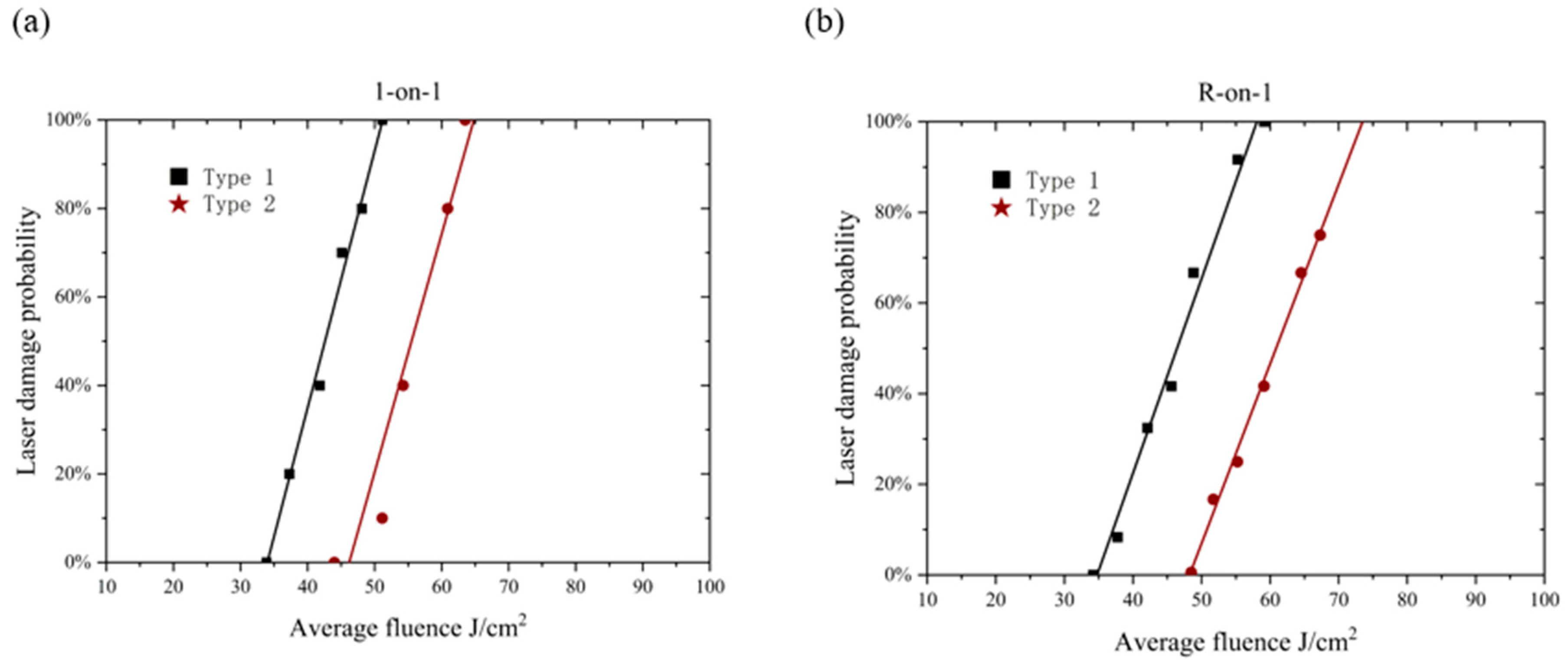
The damage threshold test results for the samples are shown in
Figure 3 and
Table 3. In both test experiments, the type 1 damage threshold was lower than the type 2 damage threshold; in the 1-on-1 test, the type 1 damage threshold was 34.41 J/cm
2 and the type 2 damage threshold was 45.76 J/cm
2; in the R-on-1 test, the type 1 damage threshold was 34.94 J/cm
2 and the type 2 damage threshold was 48.05 J/cm
2. The R-on-1 test is slightly higher than the 1-on-1 test in both types of damage thresholds. The damage thresholds of the samples were more stable and the samples were of good quality. The laser irradiation produced different damage patterns for the two types of damage, and the subsequent experimental changes were also different.
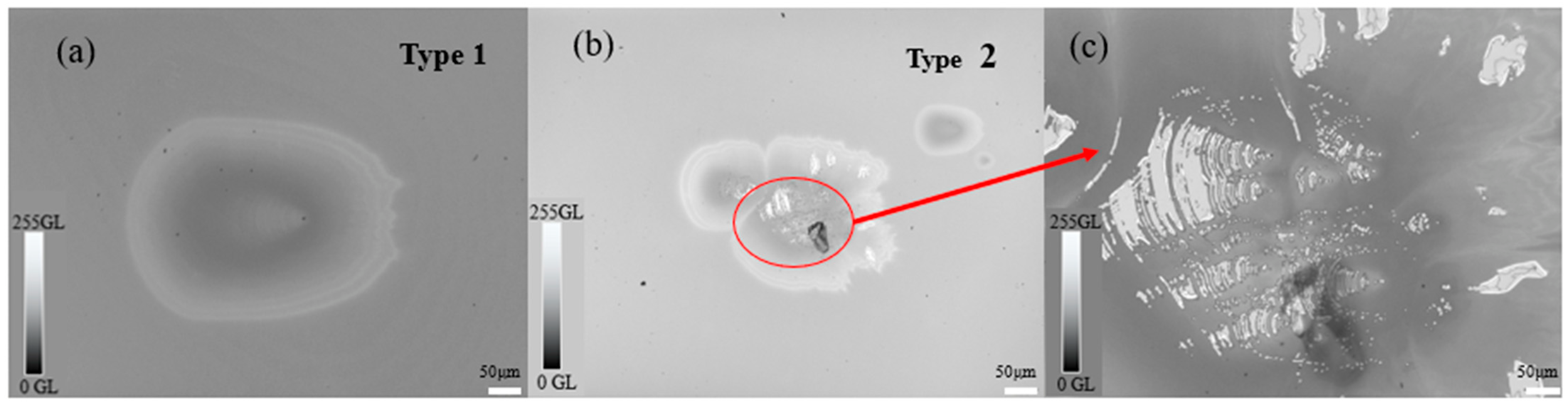
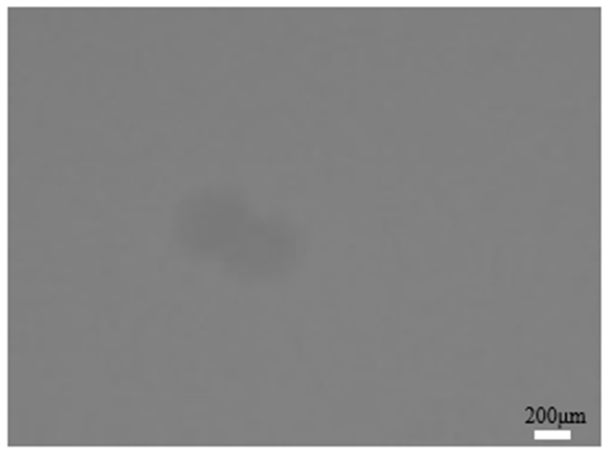
Type 1 damage is usually smaller in size and more dispersed. The main manifestation is the discoloration of the film layer, which becomes white or gray, and the color difference of the damaged area of the film layer can be observed under a high magnification microscope. In the experiments, the laser was incident at 45° to the sample surface, and the damage tended to be oval in shape. In
Figure 4a, the edges of the damaged film surface are higher than the unirradiated film surface, and the area near the center is concave.
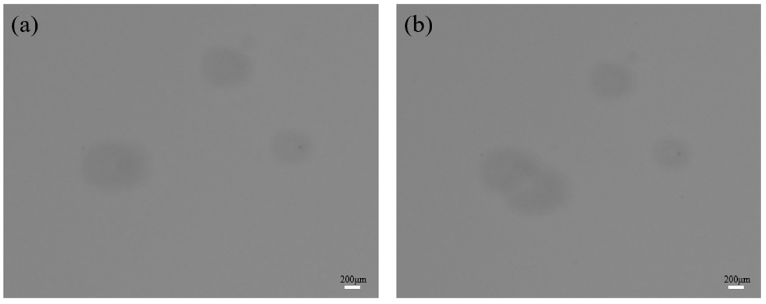
Type 2 damage is often seen at higher laser irradiation fluxes and is mainly pit-like, and the damaged area may be small or large with membrane layer detachment, often accompanied by ablation marks at the edge of the damage. In
Figure 4b,c, the film layer fracture edge is clear, representing stress damage, and the height of the damage site is lower than that of the undamaged film layer. Melt-like damage appears in
Figure 4c.
3.2. Initial Damage
The two types of damage exhibited different morphologies, and it was observed that some initial damage points would increase in the damage area as the number of strikes increased, while some damage points did not undergo any further changes. The subsequent growth of microscopically similar damage sites may be very different. In order to further investigate the difference in damage performance between the two types of damage and the causes, further damage growth experiments were conducted to explore the pattern of the subsequent changes in the initial damage.
The damage growth experiment uses the same equipment, optical path, and samples as the above test experiment. The two types of damage were struck by the fundamental frequency laser at a fluence of 46.4 J/cm2, and the shape of the damage and the damaged area were recorded. The damage was irradiated several times with the same fluence laser at the damage point, and the change in damage shape and the corresponding number of shots were recorded. The initial damage at each fluence has been experimented with several times, and multiple fluences were chosen to increase gradually from below 46.4 J/cm2 to 58.9 J/cm2.
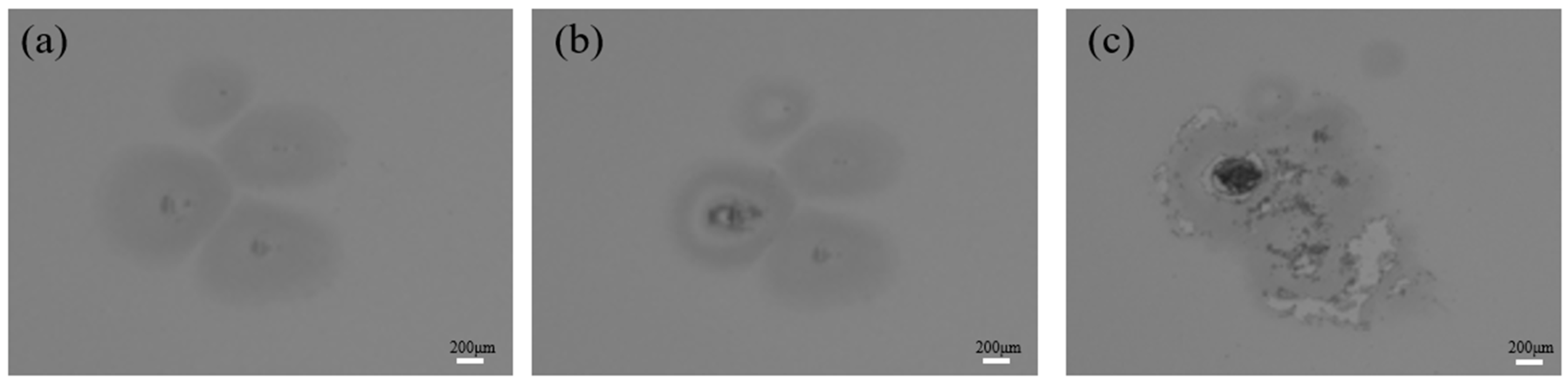
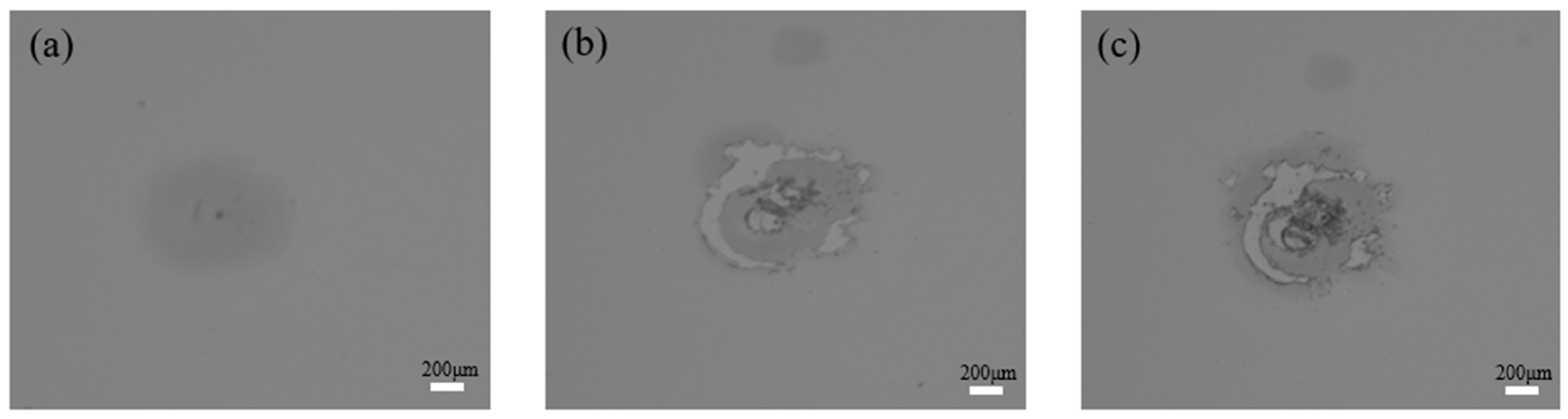
As shown in
Figure 5a, the initial damage was caused by a fluence of 46.4 J/cm
2 and the damage is of type 2. In
Figure 5b–e, the shape of the damage growth is at 43.7 J/cm
2 fluence for 1–4 hits, which is below the threshold fluence of type 2 damage. The damage grows and expands rapidly, forming a more serious shape of type 2 damage.
Figure 5f shows the initial type 1 damage caused by 46.4 J/cm
2 fluence, and
Figure 5g–j shows the damage growth morphology at 43.6 J/cm
2 fluence for 5, 10, 15, and 20 hits, and it can be observed that the shape of the damage has not changed.
It can be seen that the presence of the initial damage, especially type 2 damage, may lead to a decrease in the damage threshold, and can lead to a rapid increase in damage. In this regard, multiple sets of experiments were conducted for initial type 1 damage and type 2 damage by changing the laser irradiation flux.
3.2.1. Impairment Growth for Type 1 Damage
As shown in
Figure 6,
Figure 7 and
Figure 8, Type 1 damage subsequently uses 46.4 J/cm
2 fluence (initial damage formation flux) or less than this flux, but when there is laser irradiation or there are multiple irradiation cases, there is no change in the damage.
In the subsequent striking process that uses a fluence greater than 46.4 J/cm2 but less than 46.8 J/cm2, the area change is small. Either the area does not increase in the process of multiple strikes or any increase is not significant, and the growth of damage morphology is of type 1.
If the irradiation fluence is greater than 46.8 J/cm2 (damage transformation threshold), part of type 1 damage will grow into type 2 damage, and the probability of growth increases as the laser fluence increases.
Both the initial damage formation flux and the damage transformation threshold flux of type 1 damage are much larger than the threshold of type 1 damage and larger than the threshold of type 2 damage, and it can be assumed that if the laser flux is not increased significantly after the occurrence of type 1 damage, the damage will not grow and becomes more stable. This suggests that the formation of type 1 damage may be related to the formation of plasma caused by defects and contamination on the surface during laser irradiation. High-temperature plasma scalded film layers produce type 1 damage, and with the laser energy increases, the maximum damage size of the scald increases [
16].
3.2.2. Impairment Growth for Type 2 Damage
From
Figure 9,
Figure 10 and
Figure 11, type 2 damage causes damage growth at fluxes above 26.3 J/cm
2, which is much less than the type 2 damage threshold (and also less than the type 1 damage threshold). As the fluence increases, a small number of shots can cause a rapid increase in damage. This suggests that type 2 damage is often the result of thermal effects and thermal stress from laser irradiation.
Type 2 damage is caused by the presence of film fragmentation, faulting, and reduced reflectivity, which intensifies light reflection and film absorption, leading to increased subsequent damage, and rapid growth of the damage site to its maximum area at a value below the type 2 damage threshold. The damage threshold was tested in the area around the occurrence of type 2 damage, and compared to the undamaged sample, the damage threshold decreased by 44%, demonstrating the increased absorption of laser light in this area.
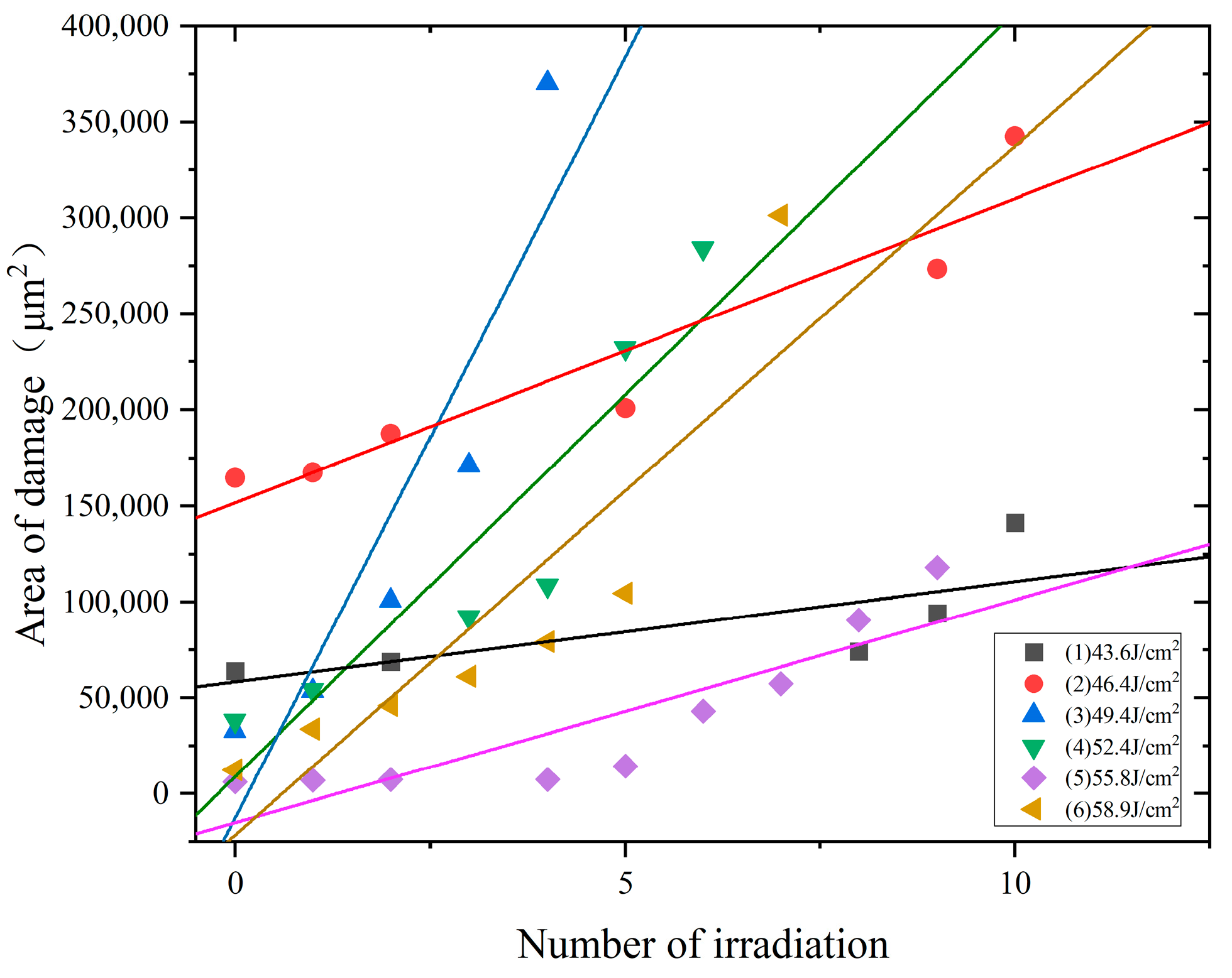
As shown in
Figure 12, with the increase in the number of laser irradiations, the damaged area increases, and eventually, there is an upper limit to the damaged area, after which the damaged area remains unchanged and does not continue to grow, a phenomenon that may be related to the effective area of the laser spot size.
The slope of the fitting curve under different fluxes in
Figure 12 can be observed, with the increase of laser irradiation flux, the damage area increases first and then decreases. The maximum growth rate of the damaged area was observed near the fluence of damage formation. The growth rate of the damaged area under the fluence of 58.9 J/cm
2 was greater than 55.8 J/cm
2, which was considered to be too large a fluence, resulting in new damage to the sample. Regardless of the size of the initial damage area, whenever type 2 damage is produced, the damaged area grows rapidly under shorter hit times.
In the experiments, the initial damage under subsequent laser irradiation showed an area growth phenomenon, and the area growth occurred both below and above the formation flux at the damage point. When the irradiation energy reaches a certain amount, a few pulses are sufficient to intensify the microdamage inside the film layer, which is macroscopically manifested as damage growth.
Therefore, further laser irradiation should be avoided for areas where damage craters occur to avoid damage area growth. If a damage point is generated, the damaged area will expand rapidly at the original fluence, leading to fracture damage of the film layer. In contrast, a small amount of one type of damage occurs, which can be temporarily left untreated if subsequently irradiated with the same fluence, and the damage will not continue to expand.
4. Discussions
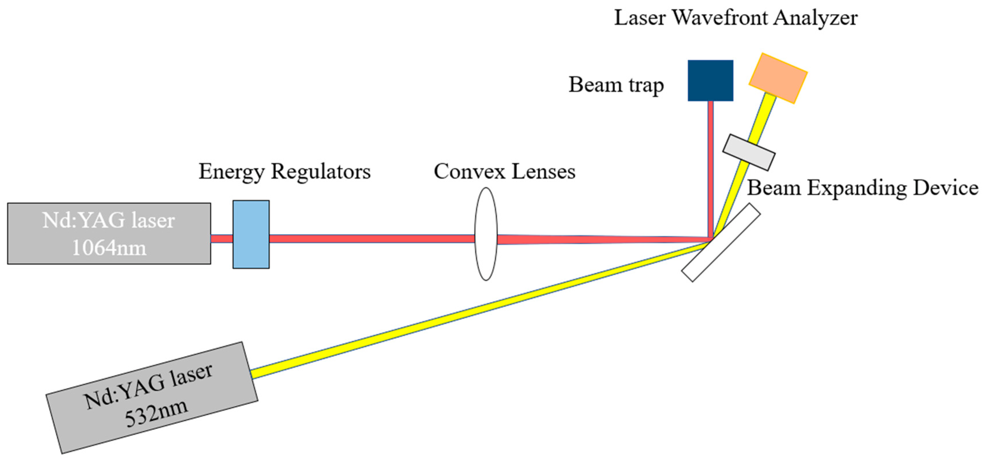
In the experiments, it was observed that the two types of damage had different growth characteristics under subsequent irradiation: type 1 damage is more stable; the second type of damage grows when irradiated by laser light well below the damage threshold. The difference between the two types of damage may be due to the corresponding changes in the sample before and after laser irradiation. In order to analyze the reasons for the variability of the two types of damage, we tested the change in the reflective surface shape of the sample using an online experiment, and the experimental setup is shown in
Figure 13.
A Nd:YAG laser with an output wavelength of 532 nm was used, the wavefront data test beam was output at the damage point and passed through the beam expander into the laser wavefront analysis device, which gave the wavefront data for the sample. The damage samples, type I damage samples, and type II damage samples were tested by this device, and the experimental results are shown in
Figure 14 and
Figure 15.
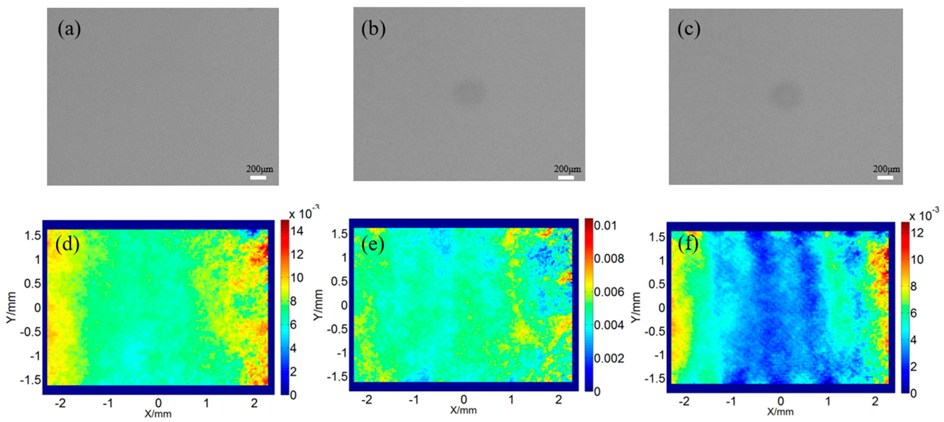
Figure 14 shows the microstructure of type 1 damage and the results of micro-zone wavefront tests, where (a) shows the microstructure of the sample before laser irradiation, (b) shows the shape of type 1 damage produced after laser irradiation, and (c) shows the shape of damage produced after re-irradiation at the same fluence.
Figure 14d–f shows the results of wavefront tests in the microregion corresponding to
Figure 14a−c. Comparing
Figure 14b,c, the damage did not grow after re-irradiation after the laser produced type 1 damage. Corresponding to
Figure 14e,f, the wavefront of the sample changed before and after the damage was produced, and the re-irradiation after the damage caused further changes in the sample, but the actual maximum change was only 0.006λ.
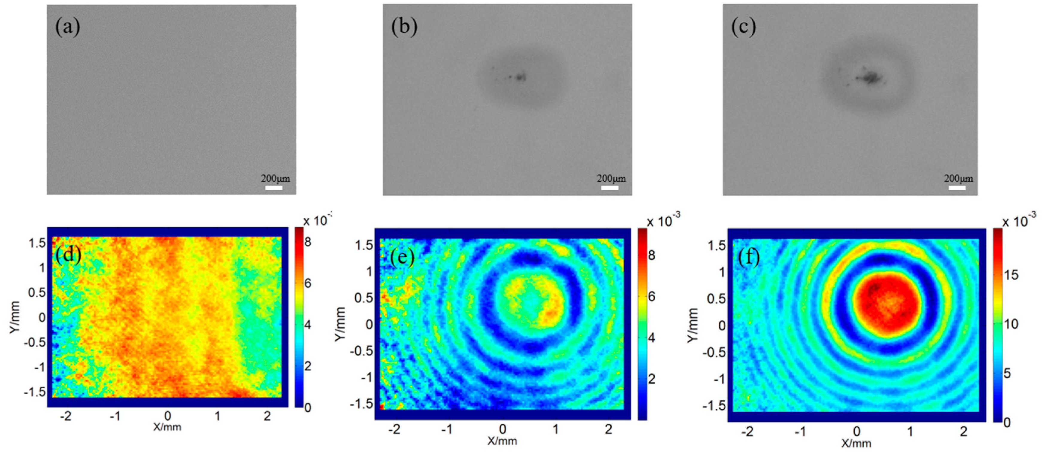
Figure 15 shows the microscopic morphology of the type 2 damage and the micro-zone wavefront test results, where (a) shows the microscopic morphology of the sample before laser irradiation, (b) shows the morphology of the type 2 damage after laser irradiation, and (c) shows the morphology of the damage after re-irradiation at the same fluence after damage generation.
Figure 15d−f shows the results of wavefront tests in the microregion corresponding to
Figure 15a–c. The wavefront distribution of the sample before and after the damage was produced, significantly changed the center of the damage point, and after the damage was irradiated again, the wavefront data around the damage point increased significantly, which corresponds to the growth of the damage point in
Figure 15c compared with that in
Figure 15b for the second type of damage.
From the test results, we can predict the subsequent development trend of the damage by the change of the face shape of the sample. Although the difference between the wavefront distribution after local irradiation of type 1 damage is large, the maximum intensity is only 0.006λ, which is considered as the noise distribution after zeroing the wavefront, i.e., no change in the wavefront; while the local surface shape of type 2 damage forms a wavefront deformation centered on the damage point after irradiation, and the change in the surface shape means that there is local stress here, while the spectral transmittance increases. The strengthening of the local stress leads to the fragmentation of the film layer, the fault is intensified, and the increase in spectral transmittance intensifies the reflection of light and film absorption, resulting in the subsequent intensified damage, so that the type 2 damage in the case of that below the damage threshold, the damage point will rapidly grow to the maximum area. In contrast, the face shape of the unchanged type 1 damage is not prone to increase with the number of hits.
5. Conclusions
In this paper, the laser damage performance of HfO2/SiO2 multilayer dielectric film samples were studied, it was found that there are two types of dielectric film damage, and the growth characteristics of the two types of damage under subsequent irradiation are also different.
Type 1 damage is discolored, turning white or gray, is more stable after the occurrence, and the damage will not grow without a significant increase in laser fluence. This indicates that type 1 damage formation may be related to the formation of plasma caused by defects and contamination on the surface during laser irradiation. A high-temperature plasma scalding film layer produces type 1 damage, and as the laser energy increases, the maximum size of the scalding damage increases.
Type 2 damage often occurs at higher irradiation fluxes and is manifested by the generation of crater-like damage, which may be small or large in area and may be accompanied by ablation marks on the edges of the damage. Following the occurrence of type 2 damage, a small number of hit times can cause rapid growth of the damage, which indicates that type 2 damage is often caused by the thermal effects and thermal stresses brought about by laser irradiation. Due to the presence of film fragmentation, faulting, and reduced reflectivity, the reflection of light and film absorption are intensified, leading to increased subsequent damage.
The micro-area surface shape of the damage point was tested for both types of damage, and it was found that the wavefront of the first type of damage was unchanged, while the local surface shape of the second type of damage formed a wavefront deformation centered on the damage point after irradiation, and the deformation increased with the expansion of the damage point. The experiments showed that the damage point without substantial changes in the surface shape will not continue to grow in the subsequent irradiation, and the degree of change in the surface shape can predict the growth of the damage point, the more drastic the change in surface shape, the more likely the damage point will grow rapidly in subsequent irradiation. In practice, the subsequent trend of damage can be predicted by the change of the surface shape of the sample.
Author Contributions
Conceptualization, Y.T., H.L., Y.T., F.W. and H.L.; validation, Y.T. and H.L.; analysis, Z.C., Y.T., H.L. and L.Z.; investigation, Z.C. and J.Z.; data curation, Z.C., J.Z. and Y.A.; writing–original draft preparation, Z.C.; writing–review and editing, Z.C., Y.T., H.L., M.C., J.C. and L.Z.; supervision, F.W., H.L., X.D. and L.S.; project administration, F.W., H.L. and X.D. All authors have read and agreed to the published version of the manuscript.
Funding
The authors are grateful for the support of the National Natural Science Foundation of China CNSTC (62175222, 62005258).
Data Availability Statement
The data that support the findings of this study are, available from the corresponding author upon reasonable request.
Acknowledgments
The authors acknowledge the support from the Institute of Research Center of Laser Fusion.
Conflicts of Interest
The authors declare no conflict of interest.
References
- Bercegol, H. What is laser conditioning: A review focused on dielectric multilayers. In Proceedings of the Laser-Induced Damage in Optical Materials: 1998, Boulder, CO, USA, 28 September–1 October 1998; Volume 3578, pp. 421–426. [Google Scholar]
- Stolz, C.J.; Thomas, M.D.; Griffin, A.J. BDS thin film damage competition. In Proceedings of the Boulder Damage Symposium XL Annual Symposium on Optical Materials for High Power Lasers, Boulder, CO, USA, 22–24 September 2008; Volume 7132, pp. 71320C–71327C. [Google Scholar]
- Krol, H.; Gallais, L.; Grèzes-Besset, C.; Natoli, J.-Y.; Commandré, M. Investigation of nanoprecursors threshold distribution in laser-damage testing. Opt. Commun. 2005, 256, 184–189. [Google Scholar] [CrossRef]
- Rudolph, W.; Emmert, L.; Sun, Z.; Patel, D.; Menoni, C. Laser damage in thin films—What we know and what we don’t. In Proceedings of the SPIE Laser Damage, Boulder, CO, USA, 22–25 September 2013. [Google Scholar]
- Stuart, B.C.; Feit, M.D.; Herman, S.; Rubenchik, A.M.; Shore, B.W.; Perry, M.D. Nanosecond-to-femtosecond laser-induced breakdown in dielectrics. Phys. Rev. B 1996, 53, 1749–1761. [Google Scholar] [CrossRef] [PubMed] [Green Version]
- Wu, Z.; Stolz, C.J.; Weakley, S.C.; Hughes, J.D.; Zhao, Q. Damage threshold prediction of hafnia–silica multilayer coatings by nondestructive evaluation of fluence-limiting defects. Appl. Opt. 2001, 40, 1897–1906. [Google Scholar] [CrossRef] [PubMed]
- Bloembergen, N. Role of Cracks, Pores, and Absorbing Inclusions on Laser Induced Damage Threshold at Surfaces of Transparent Dielectrics. Appl. Opt. 1973, 12, 661. [Google Scholar] [CrossRef] [PubMed]
- Bhar, G.; Chaudhary, A.; Kumbhakar, P. Study of laser induced damage threshold and effect of inclusions in some nonlinear crystals. Appl. Surf. Sci. 2000, 161, 155–162. [Google Scholar] [CrossRef]
- Cheng, X.; Tuniyazi, A.; Zhang, J.; Ding, T.; Jiao, H.; Ma, B.; Wei, Z.; Li, H.; Wang, Z. Nanosecond laser-induced damage of nodular defects in dielectric multilayer mirrors [Invited]. Appl. Opt. 2014, 53, A62–A69. [Google Scholar] [CrossRef] [PubMed]
- Manenkov, A.A.; Prokhorov, A.M. Laser-induced damage in solids. Sov. Phys. Usp. 1986, 148, 179. [Google Scholar] [CrossRef]
- Smalakys, L.; Drobužaitė, E.; Momgaudis, B.; Grigutis, R.; Melninkaitis, A. Quantitative investigation of laser-induced damage fatigue in HfO2 and ZrO2 single layer coatings. Opt. Express 2020, 28, 25335–25345. [Google Scholar] [CrossRef] [PubMed]
- Wang, H.; Qi, H.; Zhao, J.; Wang, B.; Shao, J. Transition from isolated submicrometer pits to integral ablation of HfO2 and SiO2 films under subpicosecond irradiation. Opt. Commun. 2017, 387, 214–222. [Google Scholar] [CrossRef]
- Sozet, M.; Bouillet, S.; Berthelot, J.; Neauport, J.; Lamaignère, L.; Gallais, L. Sub-picosecond laser damage growth on high reflective coatings for high power applications. Opt. Express 2017, 25, 25767–25781. [Google Scholar] [CrossRef] [PubMed] [Green Version]
- Sozet, M.; Néauport, J.; Lavastre, E.; Roquin, N.; Gallais, L.; Lamaignère, L. Sub-picosecond laser-induced damage test facility for petawatt reflective optical components characterizations. In Proceedings of the SPIE 9513, In High-Power, High-Energy, & High-Intensity Laser Technology II. Prague, Czech Republic, 13–16 April 2015. [Google Scholar]
- Smalakys, L.; Momgaudis, B.; Grigutis, R.; Kičas, S.; Melninkaitis, A. Contrasted fatigue behavior of laser-induced damage mechanisms in single layer ZrO2 optical coating. Opt. Express 2019, 27, 26088. [Google Scholar] [CrossRef] [PubMed]
- Raman, R.N.; Demos, S.G.; Shen, N.; Feigenbaum, E.; Negres, R.A.; Elhadj, S.; Rubenchik, A.M.; Matthews, M.J. Damage on fused silica optics caused by laser ablation of surface-bound microparticles. Opt. Express 2016, 24, 2634–2647. [Google Scholar] [CrossRef] [PubMed]
- Xu, C.; Li, D.; Fan, H.; Deng, J.; Qi, J.; Yi, P.; Qiang, Y. Effects of different post-treatment methods on optical properties, absorption and nanosecond laser-induced damage threshold of Ta2O5 films. Thin Solid Film. 2015, 580, 12–20. [Google Scholar] [CrossRef]
- Pu, Y.; Ma, P.; Chen, S.; Zhu, J.; Wang, G.; Pan, F.; Sun, P.; Zhu, X.; Zhu, J.; Xiao, D. Mechanism for atmosphere dependence of laser damage morphology in HfO2/SiO2 high reflective films. J. Appl. Phys. 2021, 112, 023111. [Google Scholar] [CrossRef]
- Harthcock, C.; Qiu, S.R.; Mirkarimi, P.B.; Negres, R.A.; Guss, G.; Menor, M.G.; Bhowmik, G.; Huang, M. Origin and effect of film sub-stoichiometry on ultraviolet, ns-laser damage resistance of hafnia single layers. Opt. Mater. Express 2020, 10, 937–951. [Google Scholar] [CrossRef]
- Abromavičius, G.; Kičas, S.; Buzelis, R. High temperature annealing effects on spectral, microstructural and laser damage resistance properties of sputtered HfO2 and HfO2-SiO2 mixture-based UV mirrors. Opt. Mater. 2019, 95, 109245. [Google Scholar] [CrossRef]
- Jena, S.; Tokas, R.B.; Rao, K.D.; Thakur, S.; Sahoo, N.K. Annealing effects on microstructure and laser-induced damage threshold of HfO2/SiO2 multilayer mirrors. Appl. Opt. 2016, 55, 6108–6114. [Google Scholar] [CrossRef] [PubMed]
- Zhao, Z.; Sun, J.; Zhu, M.; Zeng, T.; Yin, C.; Yi, K.; Zhao, Y.; Cui, Y.; Shao, J. Research to improve the optical performance and laser-induced damage threshold of hafnium oxide/silica dichroic coatings. Opt. Mater. 2021, 113, 110890. [Google Scholar] [CrossRef]
- Al-Kuhaili, M.F. Optical properties of hafnium oxide thin films and their application in energy-efficient windows. Opt. Mater. 2004, 27, 383–387. [Google Scholar] [CrossRef]
- Malitson, I.H. Interspecimen comparison of the refractive index of fused silica. J. Opt. Soc. Am. 1965, 55, 1205–1209. [Google Scholar] [CrossRef]
Figure 1.
Sample surface testing chart.
Figure 1.
Sample surface testing chart.
Figure 2.
Damage experimental setup and light spot measurement. (a) Damage experimental setup; (b) light spot; and (c) pulse width.
Figure 2.
Damage experimental setup and light spot measurement. (a) Damage experimental setup; (b) light spot; and (c) pulse width.
Figure 3.
(a) The 1-on-1 experimental damage threshold curve and (b) R-on-1 experimental damage threshold curve.
Figure 3.
(a) The 1-on-1 experimental damage threshold curve and (b) R-on-1 experimental damage threshold curve.
Figure 4.
Microtopography of the sample damage. (a) Type 1; (b) type 2; and (c) local magnification of type 2 damage.
Figure 4.
Microtopography of the sample damage. (a) Type 1; (b) type 2; and (c) local magnification of type 2 damage.
Figure 5.
Damage growth morphology of 46.4 J/cm2 experiment. (a) Initial damage morphology of type 2; (b–e) damage growth morphology of type 2; (f) initial damage morphology of type 1; and (g–j) damage growth morphology of type 1.
Figure 5.
Damage growth morphology of 46.4 J/cm2 experiment. (a) Initial damage morphology of type 2; (b–e) damage growth morphology of type 2; (f) initial damage morphology of type 1; and (g–j) damage growth morphology of type 1.
Figure 6.
Damage profile of the low flux multiple irradiations.
Figure 6.
Damage profile of the low flux multiple irradiations.
Figure 7.
Damage profile of the high flux multiple irradiations. (a) Initial damage morphology and (b) damage profile of multiple irradiations.
Figure 7.
Damage profile of the high flux multiple irradiations. (a) Initial damage morphology and (b) damage profile of multiple irradiations.
Figure 8.
The threshold of type 1 damage transforming into type 2 damage.
Figure 8.
The threshold of type 1 damage transforming into type 2 damage.
Figure 9.
Damage profile of low flux multiple irradiations. (a) Initial damage morphology; (b) 5 irradiations; and (c) 10 irradiations.
Figure 9.
Damage profile of low flux multiple irradiations. (a) Initial damage morphology; (b) 5 irradiations; and (c) 10 irradiations.
Figure 10.
Damage profile of high flux multiple irradiations. (a) Initial damage morphology; (b) 2 irradiations; and (c) 3 irradiations.
Figure 10.
Damage profile of high flux multiple irradiations. (a) Initial damage morphology; (b) 2 irradiations; and (c) 3 irradiations.
Figure 11.
Growth threshold of type 2 damage.
Figure 11.
Growth threshold of type 2 damage.
Figure 12.
Fitting curve of the damaged area.
Figure 12.
Fitting curve of the damaged area.
Figure 13.
Sample surface shape test device.
Figure 13.
Sample surface shape test device.
Figure 14.
The experimental results of type 1 damage microscopic morphology and micro-surface shape test. (a) Pre-irradiation; (b) damage; (c) after 1 irradiation at the same flux; (d) pre-irradiation; (e) damage; and (f) after 1 irradiation at the same flux.
Figure 14.
The experimental results of type 1 damage microscopic morphology and micro-surface shape test. (a) Pre-irradiation; (b) damage; (c) after 1 irradiation at the same flux; (d) pre-irradiation; (e) damage; and (f) after 1 irradiation at the same flux.
Figure 15.
The experimental results of type 2 damage microscopic morphology and micro-surface shape test. (a) Pre-irradiation; (b) damage; (c) after 1 irradiation at the same flux; (d) pre-irradiation; (e) damage; and (f) after 1 irradiation at the same flux.
Figure 15.
The experimental results of type 2 damage microscopic morphology and micro-surface shape test. (a) Pre-irradiation; (b) damage; (c) after 1 irradiation at the same flux; (d) pre-irradiation; (e) damage; and (f) after 1 irradiation at the same flux.
Table 1.
Refractive index of different wavelengths (HfO
2) [
23].
Table 1.
Refractive index of different wavelengths (HfO
2) [
23].
| Material | HfO2 |
|---|
| Lambda (nm) | 1064 | 1053 | 700 | 400 | 375 | 355 | 351 |
| Refractive index | 1.8810 | 1.8811 | 1.8902 | 1.9369 | 1.9490 | 1.9614 | 1.9642 |
Table 2.
Refractive index of different wavelengths (SiO
2) [
24].
Table 2.
Refractive index of different wavelengths (SiO
2) [
24].
| Material | SiO2 |
|---|
| Lambda (nm) | 1064 | 1053 | 700 | 400 | 375 | 355 | 351 |
| Refractive index | 1.4496 | 1.4498 | 1.4553 | 1.4701 | 1.4731 | 1.4761 | 1.4767 |
Table 3.
The damage threshold of the sample.
Table 3.
The damage threshold of the sample.
| | Type 1 | Type 2 |
|---|
| 1-on-1 | 34.41 J/cm2 | 45.76 J/cm2 |
| R-on-1 | 34.94 J/cm2 | 48.05 J/cm2 |
| Disclaimer/Publisher’s Note: The statements, opinions and data contained in all publications are solely those of the individual author(s) and contributor(s) and not of MDPI and/or the editor(s). MDPI and/or the editor(s) disclaim responsibility for any injury to people or property resulting from any ideas, methods, instructions or products referred to in the content. |
© 2023 by the authors. Licensee MDPI, Basel, Switzerland. This article is an open access article distributed under the terms and conditions of the Creative Commons Attribution (CC BY) license (https://creativecommons.org/licenses/by/4.0/).


