
Optoelectronic Simulations of InGaN-Based Green Micro-Resonant Cavity Light-Emitting Diodes with Staggered Multiple Quantum Wells
 , and
, and 
Abstract
:1. Introduction
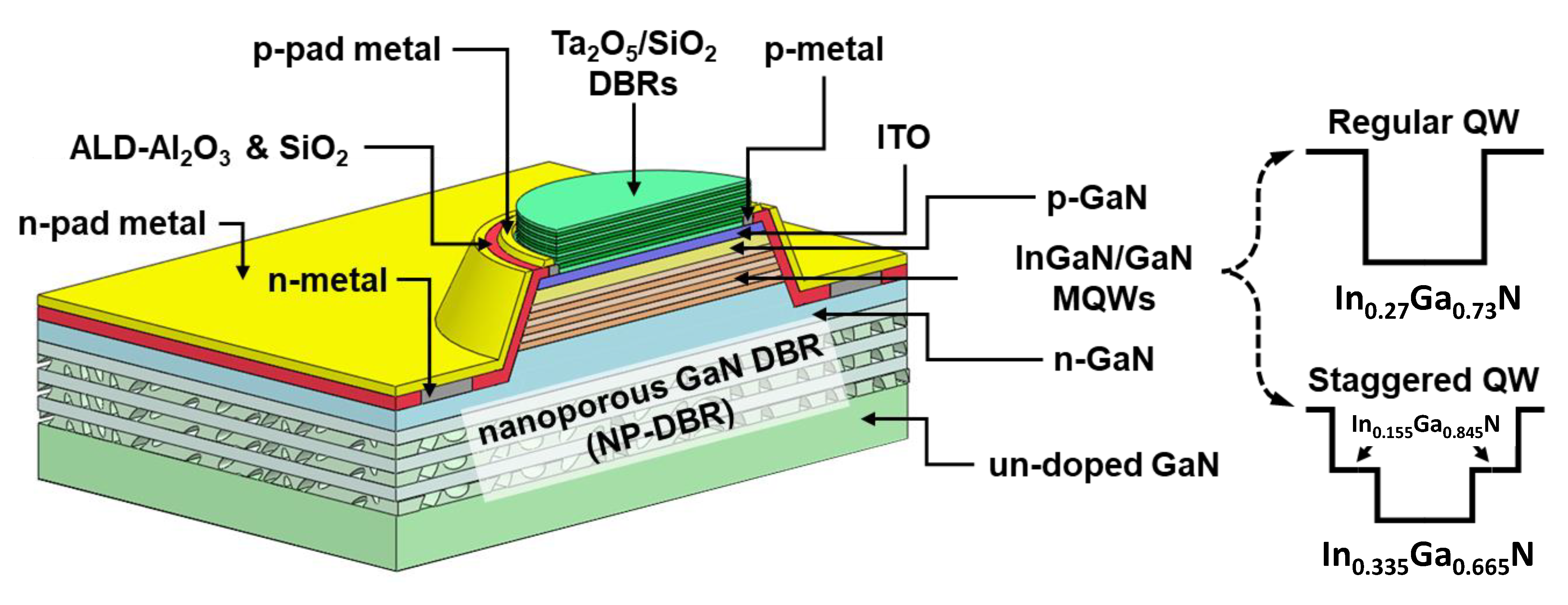
2. Experiments
3. Simulated Method and Structure Definition
4. Result and Discussion
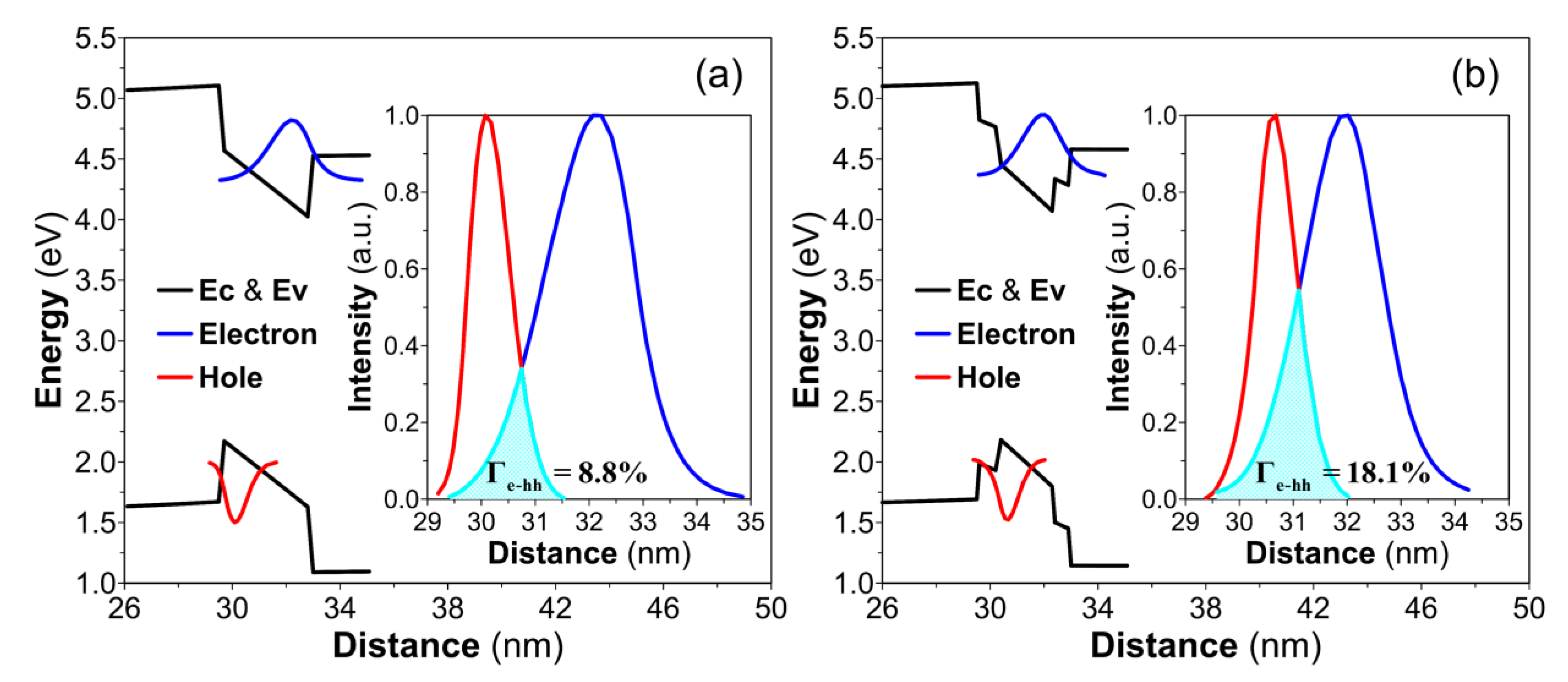
4.1. Wavefunction Overlap and Peak Wavelength Shift
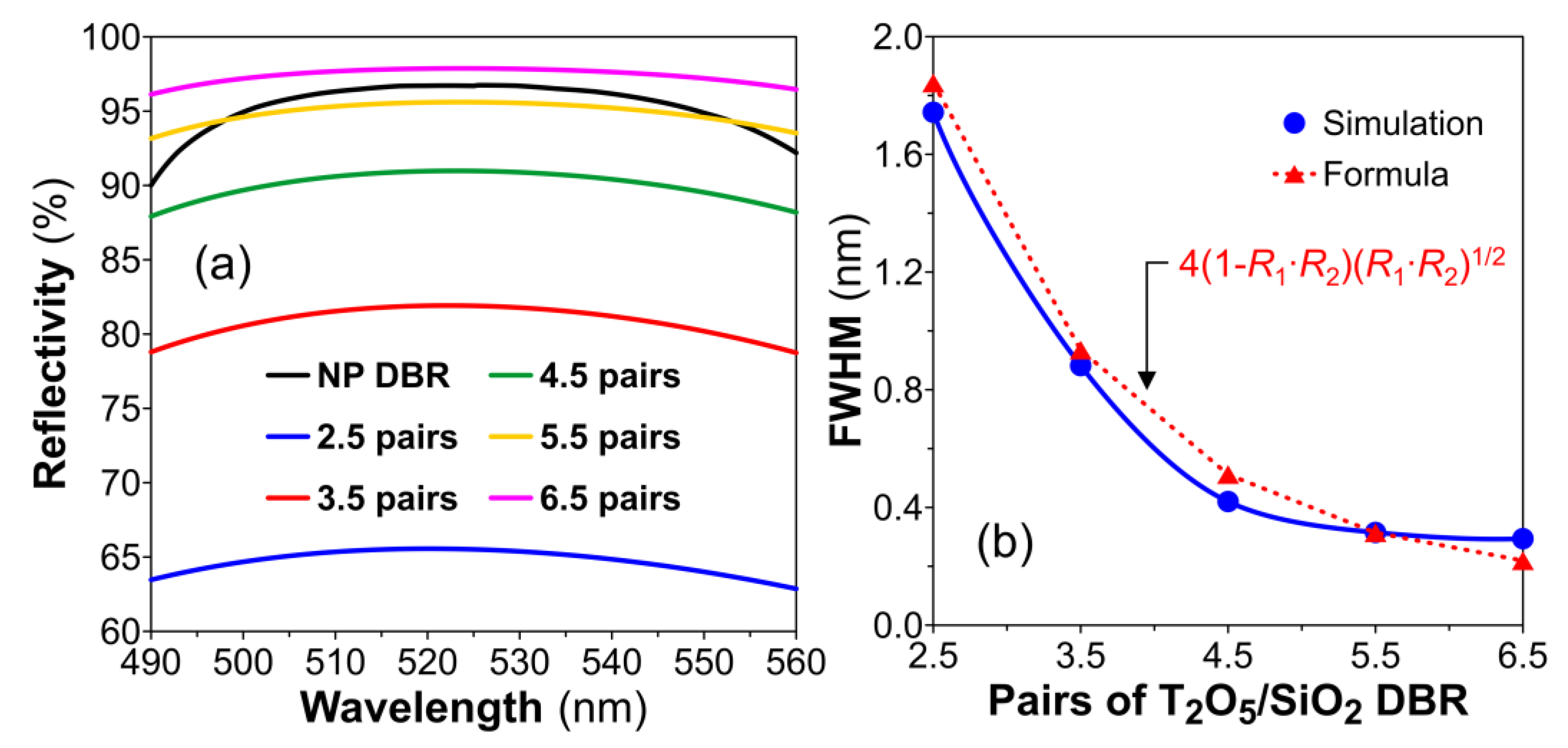
4.2. Reflectivity Spectrum and FWHM
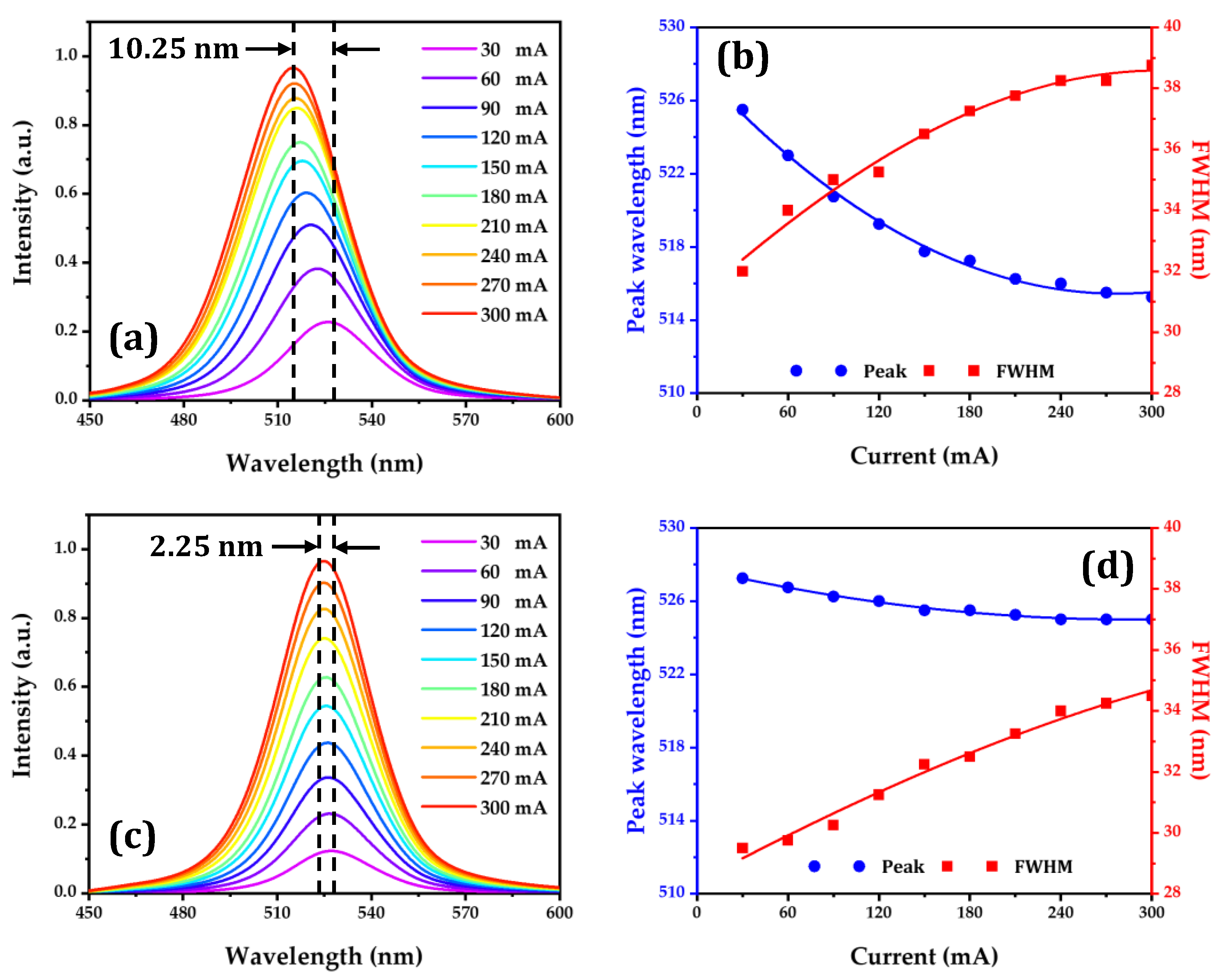
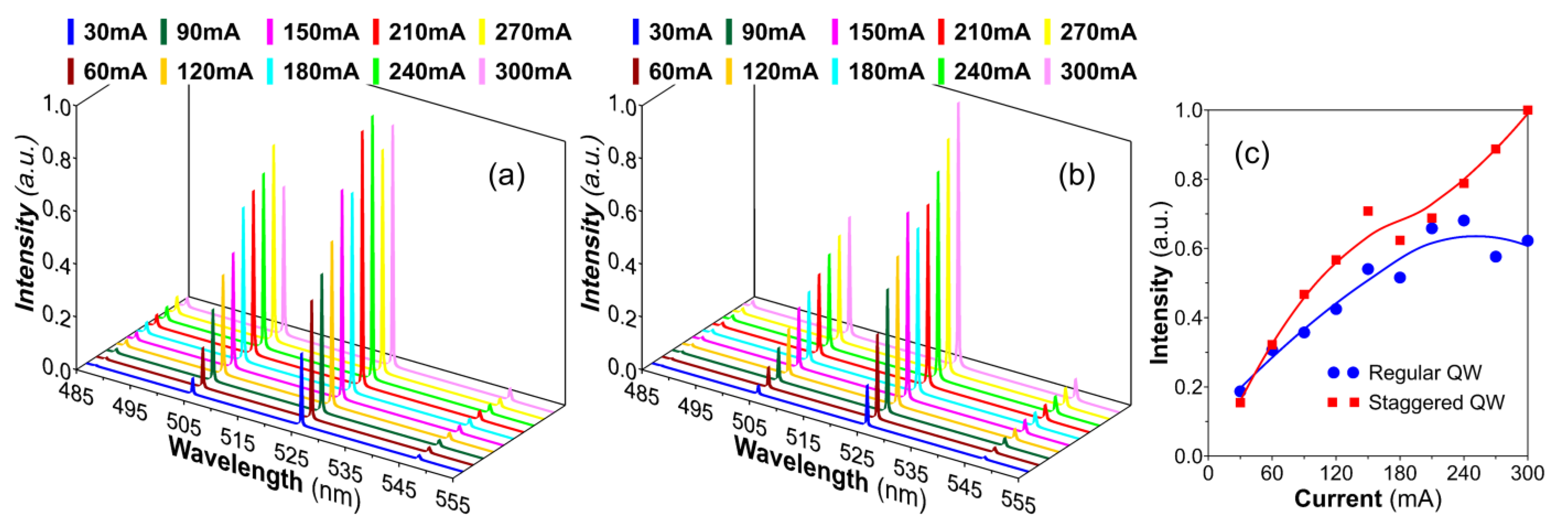
4.3. Emission Spectrum of µ-RCLED
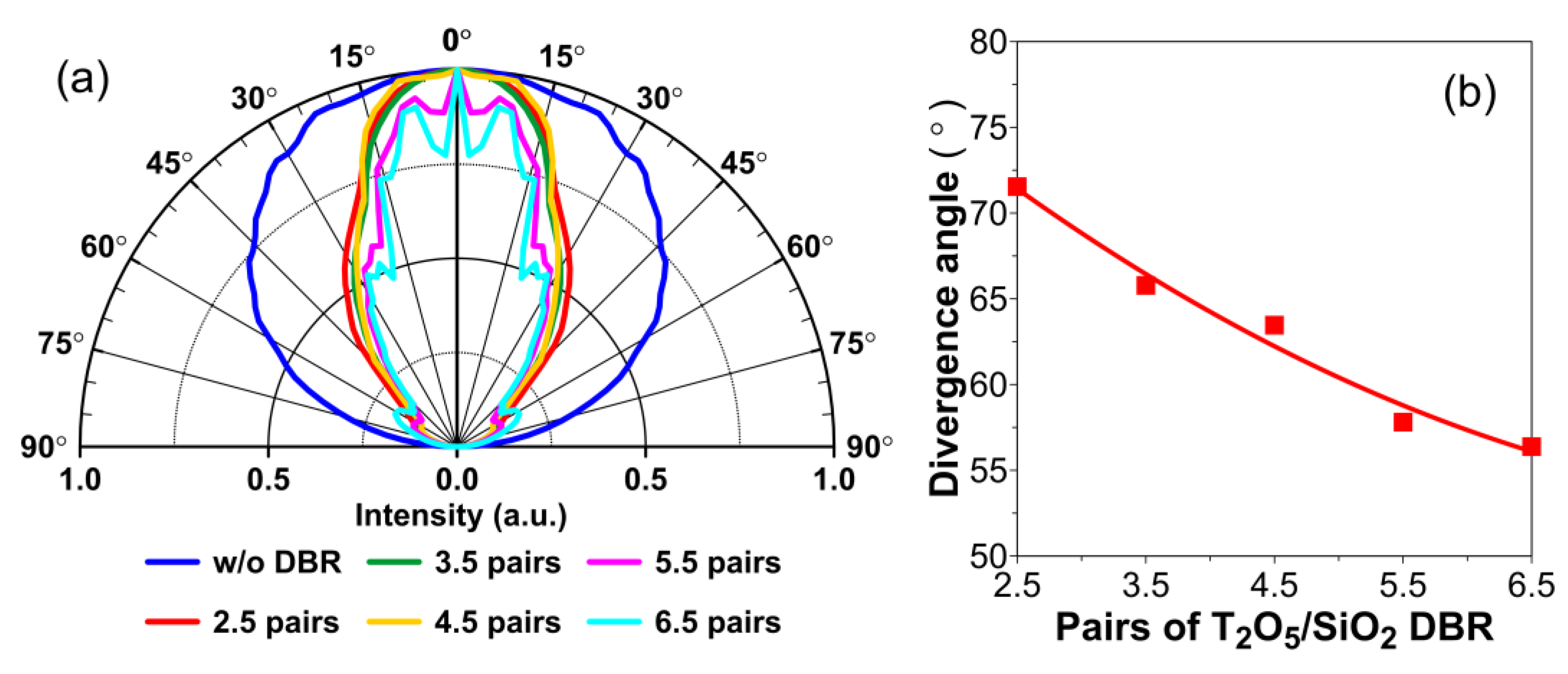
4.4. Divergence Angle of µ-RCLED with Staggered MQWs
5. Conclusions
Author Contributions
Funding
Institutional Review Board Statement
Informed Consent Statement
Data Availability Statement
Acknowledgments
Conflicts of Interest
References
- Chou, H.-H.; Huang, W.-T. Asymmetrical bidirectional optical wireless communication system based on a transmissive 1D LC-SLM for NG-PON2. Opt. Lett. 2020, 45, 4543–4546. [Google Scholar] [CrossRef]
- Chou, H.H.; Huang, W.T. Wavelength Tunable Asymmetric B-OWC System Based on Self-Injection Locking for TDM-PONs. IEEE Photonics Technol. Lett. 2021, 33, 370–372. [Google Scholar] [CrossRef]
- Li, C.; Lu, H.; Tsai, W.; Wang, Z.; Hung, C.; Su, C.; Lu, Y. A 5 m/25 Gbps Underwater Wireless Optical Communication System. IEEE Photonics J. 2018, 10, 1–9. [Google Scholar] [CrossRef]
- Wu, T.; Yue, L.; Huang, Y.-M.; Liu, M.; James Singh, K.; Lin, W.; Lu, T.; Zheng, X.; Zhou, Z.; Kuo, H.-C.; et al. A highly stable full-color display device with VLC application potential using semipolar micro-LEDs and all-inorganic encapsulated perovskite nanocrystal. Photon. Res. 2021, 9, 2132. [Google Scholar] [CrossRef]
- Do, T.-H.; Yoo, M. An in-Depth Survey of Visible Light Communication Based Positioning Systems. Sensors 2016, 16, 678. [Google Scholar] [CrossRef] [PubMed] [Green Version]
- Yu, T.-C.; Huang, W.-T.; Lee, W.-B.; Chow, C.-W.; Chang, S.-W.; Kuo, H.-C. Visible Light Communication System Technology Review: Devices, Architectures, and Applications. Crystals 2021, 11, 1098. [Google Scholar] [CrossRef]
- Peng, C.-Y.; Huang, W.-T.; Lu, Z.-K.; Chen, S.-C.; Kuo, H.-C. Design of High-Power Red VCSEL on a Removable Substrate. Photonics 2022, 9, 763. [Google Scholar] [CrossRef]
- Huang, W.-T.; Peng, C.-Y.; Chiang, H.; Huang, Y.-M.; Singh, K.J.; Lee, W.-B.; Chow, C.-W.; Chen, S.-C.; Kuo, H.-C. Toward high-bandwidth yellow-green micro-LEDs utilizing nanoporous distributed Bragg reflectors for visible light communication. Photon. Res. 2022, 10, 1810–1818. [Google Scholar] [CrossRef]
- Takeuchi, T.; Amano, H.; Akasaki, I. Theoretical Study of Orientation Dependence of Piezoelectric Effects in Wurtzite Strained GaInN/GaN Heterostructures and Quantum Wells. Jpn. J. Appl. Phys. 2000, 39, 413. [Google Scholar] [CrossRef]
- Piprek, J. Efficiency droop in nitride-based light-emitting diodes. Phys. Status Solidi A 2010, 207, 2217–2225. [Google Scholar] [CrossRef]
- Huang, Y.-M.; Peng, C.-Y.; Miao, W.-C.; Chiang, H.; Lee, T.-Y.; Chang, Y.-H.; Singh, K.J.; Iida, Z.D.; Horng, R.-H.; Chow, C.-W.; et al. High-efficiency InGaN red micro-LEDs for visible light communication. Photon. Res. 2022, 10, 1978–1986. [Google Scholar] [CrossRef]
- Chen, S.-W.H.; Huang, Y.-M.; Chang, Y.-H.; Lin, Y.; Liou, F.-J.; Hsu, Y.-C.; Song, J.; Choi, J.; Chow, C.-W.; Lin, C.-C.; et al. High-Bandwidth Green Semipolar (20–21) InGaN/GaN Micro Light-Emitting Diodes for Visible Light Communication. ACS Photonics 2020, 7, 2228–2235. [Google Scholar] [CrossRef]
- Arif, R.A.; Ee, Y.-K.; Tansu, N. Polarization engineering via staggered InGaN quantum wells for radiative efficiency enhancement of light emitting diodes. Appl. Phys. Lett. 2007, 91, 091110. [Google Scholar] [CrossRef] [Green Version]
- Zhao, H.; Arif, R.A.; Tansu, N. Design Analysis of Staggered InGaN Quantum Wells Light-Emitting Diodes at 500–540 nm. IEEE J. Sel. Top. Quantum Electron. 2009, 15, 1104–1114. [Google Scholar] [CrossRef]
- Schubert, E.F.; Hunt, N.E.J.; Micovic, M.; Malik, R.J.; Sivco, D.L.; Cho, A.Y.; Zydzik, G.J. Highly Efficient Light-Emitting Diodes with Microcavities. Science 1994, 265, 943–945. [Google Scholar] [CrossRef]
- Song, Y.-K.; Diagne, M.; Zhou, H.; Nurmikko, A.V.; Carter-Coman, C.; Kern, R.S.; Kish, F.A.; Krames, M.R. A vertical injection blue light emitting diode in substrate separated InGaN heterostructures. Appl. Phys. Lett. 1999, 74, 3720–3722. [Google Scholar] [CrossRef]
- Horng, R.H.; Wei-Kai, W.; Shin-Yung, H.; Dong-Sing, W. Effect of resonant cavity in wafer-bonded Green InGaN LED with dielectric and silver mirrors. IEEE Photonics Technol. Lett. 2006, 18, 457–459. [Google Scholar] [CrossRef]
- Zhao, S.; Xu, B.; Zhao, Z.; Gu, D.; Zhang, Y.; Lv, W.; Lv, X. Gallium nitride-based resonant cavity light-emitting diode with single-longitudinal-mode emission. Opt. Lett. 2022, 47, 4616–4619. [Google Scholar] [CrossRef]
- Hong, K.-B.; Huang, W.-T.; Hsu, W.-C.; Tu, C.-C.; Kuo, H.-C. Investigation of InGaN-Based Green Micro-Photonic-Crystal- Light-Emitting-Diodes with Bottom, Nanoporous, Distributed Bragg Reflectors. Photonics 2022, 9, 939. [Google Scholar] [CrossRef]
- Gong, Z.; Jin, S.; Chen, Y.; McKendry, J.; Massoubre, D.; Watson, I.M.; Gu, E.; Dawson, M.D. Size-dependent light output, spectral shift, and self-heating of 400 nm InGaN light-emitting diodes. J. Appl. Phys. 2010, 107, 013103. [Google Scholar] [CrossRef]
- Sarkar, N.; Ghosh, S. Temperature dependent band gap shrinkage in GaN: Role of electron–phonon interaction. Solid State Commun. 2009, 149, 1288–1291. [Google Scholar] [CrossRef]
- Auvergne, D.; Camassel, J.; Mathieu, H. Band-gap shrinkage of semiconductors. Phys. Rev. B 1975, 11, 2251–2259. [Google Scholar] [CrossRef]
- Haemmer, M.; Roycroft, B.; Akhter, M.; Dinh, D.V.; Quan, Z.; Zhao, J.; Parbrook, P.J.; Corbett, B. Size-Dependent Bandwidth of Semipolar (11-22) Light-Emitting-Diodes. IEEE Photonics Technol. Lett. 2018, 30, 439–442. [Google Scholar] [CrossRef]
- Tian, P.; McKendry, J.J.D.; Gong, Z.; Guilhabert, B.; Watson, I.M.; Gu, E.; Chen, Z.; Zhang, G.; Dawson, M.D. Size-dependent efficiency and efficiency droop of blue InGaN micro-light emitting diodes. Appl. Phys. Lett. 2012, 101, 231110. [Google Scholar] [CrossRef]
- Lee, K.J.; Oh, S.; Kim, S.-J.; Yim, S.-Y.; Myoung, N.; Lee, K.; Kim, J.S.; Jung, S.H.; Chung, T.-H.; Park, S.-J. Enhanced optical output in InGaN/GaN light-emitting diodes by tailored refractive index of nanoporous GaN. Nanotechnology 2019, 30, 415301. [Google Scholar] [CrossRef] [PubMed]
- Yoldas, B.E.; Partlow, D.P. Formation of broad band antireflective coatings on fused silica for high power laser applications. Thin Solid Film. 1985, 129, 1–14. [Google Scholar] [CrossRef]
- Mao, P.; Sun, F.; Yao, H.; Chen, J.; Zhao, B.; Xie, B.; Han, M.; Wang, G. Extraction of light trapped due to total internal reflection using porous high refractive index nanoparticle films. Nanoscale 2014, 6, 8177–8184. [Google Scholar] [CrossRef] [Green Version]
- Arif, R.A.; Zhao, H.; Ee, Y.K.; Tansu, N. Spontaneous Emission and Characteristics of Staggered InGaN Quantum-Well Light-Emitting Diodes. IEEE J. Quantum Electron. 2008, 44, 573–580. [Google Scholar] [CrossRef]
- Stacy, W.; Mueller, G.; Reitze, D.; Tanner, D.B.; Whiting, B.F. Linewidth-broadened Fabry–Perot cavities within future gravitational wave detectors. Class. Quantum Gravity 2004, 21, S1031. [Google Scholar] [CrossRef]
- Butté, R.; Christmann, G.; Feltin, E.; Castiglia, A.; Levrat, J.; Cosendey, G.; Altoukhov, A.; Carlin, J.-F.; Grandjean, N. Room Temperature Polariton Lasing in III-Nitride Microcavities: A Comparison with Blue GaN-Based Vertical Cavity Surface Emitting Lasers; SPIE: Washington, DC, USA, 2009; Volume 7216. [Google Scholar]
- Zhao, G.Y.; Ishikawa, H.; Yu, G.; Egawa, T.; Watanabe, J.; Soga, T.; Jimbo, T.; Umeno, M. Thermo-optical nonlinearity of GaN grown by metalorganic chemical- vapor deposition. Appl. Phys. Lett. 1998, 73, 22–24. [Google Scholar] [CrossRef]


Disclaimer/Publisher’s Note: The statements, opinions and data contained in all publications are solely those of the individual author(s) and contributor(s) and not of MDPI and/or the editor(s). MDPI and/or the editor(s) disclaim responsibility for any injury to people or property resulting from any ideas, methods, instructions or products referred to in the content. |
© 2023 by the authors. Licensee MDPI, Basel, Switzerland. This article is an open access article distributed under the terms and conditions of the Creative Commons Attribution (CC BY) license (https://creativecommons.org/licenses/by/4.0/).
Share and Cite
Hsieh, T.-H.; Huang, W.-T.; Hong, K.-B.; Lee, T.-Y.; Bai, Y.-H.; Pai, Y.-H.; Tu, C.-C.; Huang, C.-H.; Li, Y.; Kuo, H.-C. Optoelectronic Simulations of InGaN-Based Green Micro-Resonant Cavity Light-Emitting Diodes with Staggered Multiple Quantum Wells. Crystals 2023, 13, 572. https://doi.org/10.3390/cryst13040572
Hsieh T-H, Huang W-T, Hong K-B, Lee T-Y, Bai Y-H, Pai Y-H, Tu C-C, Huang C-H, Li Y, Kuo H-C. Optoelectronic Simulations of InGaN-Based Green Micro-Resonant Cavity Light-Emitting Diodes with Staggered Multiple Quantum Wells. Crystals. 2023; 13(4):572. https://doi.org/10.3390/cryst13040572
Chicago/Turabian StyleHsieh, Tsau-Hua, Wei-Ta Huang, Kuo-Bin Hong, Tzu-Yi Lee, Yi-Hong Bai, Yi-Hua Pai, Chang-Ching Tu, Chun-Hui Huang, Yiming Li, and Hao-Chung Kuo. 2023. "Optoelectronic Simulations of InGaN-Based Green Micro-Resonant Cavity Light-Emitting Diodes with Staggered Multiple Quantum Wells" Crystals 13, no. 4: 572. https://doi.org/10.3390/cryst13040572