Article

Effect of Grain Sizes on Electrically Assisted Micro—Filling of SUS304 Stainless Steel: Experiment and Simulation

1
School of Mechanical Engineering and Automation, Beihang University, Beijing 100191, China
2
Jiangxi Research Institute of Beihang University, Nanchang 330096, China
3
Ningbo Institute of Technology, Beihang University, Ningbo 315800, China
*
Author to whom correspondence should be addressed.
Crystals 2023, 13(1), 134; https://doi.org/10.3390/cryst13010134
Submission received: 6 December 2022 / Revised: 3 January 2023 / Accepted: 11 January 2023 / Published: 12 January 2023

Abstract

:
The filling quality of micro-feature structures has a significant impact on the forming quality of micro-channels. The electrical-assisted forming technology can effectively improve the formability of difficult-to-deform materials. In this research, the electrically driven micro-compression constitutive model of SUS304 stainless steels was established to assign grain boundary and grain interior with different material properties. An electrical–thermal–mechanical coupling model was constructed to simulate the filling process considering the effect of grain boundary and grain size. Compared to the experimental results, the simulation indicated a good agreement in microstructure characteristics and higher filling height for the fine-grained material. The increase in grain boundary density makes the resistivity of the fine grain material larger, causing the current destiny and temperature of the specimen to increase with the decrease in grain size. An ellipsoidal gradient temperature distribution is observed due to the uneven current density. Because of the high geometric dislocation density near the grain boundary, a significant dislocation pile-up causes stress to concentrate. It is observed that the deformation coordination is enhanced between the grain boundary and grain core with the decrease in grain size, thus improving the material formability and forming quality.

1. Introduction

The printed circuit heat exchanger (PCHE) has desirable heat transfer, high compactness, and small size, resulting in precise micro-channel structure and high manufacturing cost [1]. Due to its high production efficiency, little or even zero material loss, excellent product performance, high dimensional precision, no pollution, and other advantages [2], micro embossing forming technology has been widely adopted to fabricate the surface micro-structure [3]. The filling forming quality of the micro features after compression is an important factor affecting the micro-channel forming of sheet metal.
Investigations have accentuated that grain refinement contributes to meliorating the micro feature quality after micro-filling [4,5]. Qiao et al. [6] produced ultra-fine-grained (UFG) Al-1050 through equal channel angular pressing (ECAP), but the cold embossing of UFG Al-1050 resulted in a substantial failure rate of micro-scaled silicon die and insufficient filling. Kim et al. [7] investigated the imprinting process of micro features in 304 stainless steels. The experimental outcomes suggested that a large load is needed to realize the designed shape. Their research further mirrored that many problems exist, such as large forming forces, severe die failure, and low efficiency. Furthermore, Qiao et al. [6] studied filling behavior under hot working conditions. At 300 °C, UFG Al-1050 produced smoother channels than coarse-grained materials and required smaller forming pressure.
Therefore, energy-assisted methods can be used to improve the quality of the microfeatures, like imprinting with high-frequency vibration technology [8], direct heating [4], and electric heating [9]. These approaches can reduce the forming load, improve friction, and enhance the material’s formability. Xu et al. have done comprehensive research on energy field-assisted micro-filling. They prepared various UFG materials, such as AZ31B magnesium alloy [4,10], Mg-Li alloy [11,12], and pure aluminum [13,14,15], and carried out in-depth explorations of the micro-filling forming process under different grain sizes, temperatures, and pressure conditions. A series of higher-quality array micro features were produced once the ideal forming temperature and pressure were identified. However, direct heating can also lead to severe drawbacks, including subpar surface polish, limited tool life, microstructure changes, and reduced part tolerances [9]. Numerous research projects have demonstrated that the electrically assisted forming process can decrease deformation resistance, improve plasticity, reduce the springback, and regulate the microstructure, providing collaborative manufacturing with low energy consumption and high efficiency. Peng et al. [9] proposed the method of making micro-channel on a metal workpiece by using electrical-assisted embossing process (EAEP) and proved the feasibility and superiority of the new process through experiments. Mai et al. [16] analyzed the influence of filling parameters on the electric field-assisted micro-filling process. Experimental findings proved that the depth of the machining channel increases, and the stress in the workpiece decreases during the process of embossing assisted by the high-density current.
Notwithstanding, it remains challenging to statistically investigate the macro- and microscopic mechanisms in the process of energy field-assisted deformation through experiments, and too many trials may result in resource waste. A multi-field coupling finite element numerical analysis model of electrical–thermal–mechanical aspects was established to simulate the electrically assisted micro-filling forming process of stainless steel [17]. The results demonstrated that the high-density current could effectively lower the yield stress during forming and raise the forming quality. To simulate the micro-filling process at various temperatures and grain sizes, Qiao et al. [18] developed a finite element model with ANSYS and concluded that it was consistent with the experimental data [6]. Nevertheless, the properties of grain morphology are not considered in the model mentioned earlier. Wang et al. [19] created two-dimensional crystal models to simulate the single groove filling of LZ91 Mg-Li alloy with coarse and ultra-fine grains. However, they did not examine the microscopic deformation mechanism. When conducting a finite element simulation of the roll-to-plate (R2P) micro-filling process on pure copper sheets, Gao et al. [3] separated the blank into grain region and non-grain area and investigated size effect on the molding height, roll pressure, and microhardness distribution. A polycrystal filling model was developed by Wang et al. [20], taking into account friction, tool constraints, cavity width, grain size, and the cavity width to grain size ratio. Then, they examined the interaction effects of these parameters on the final filling capacity and the internal physical mechanism of deformation.
Few numerical analysis models exist for micro-filling with energy field-assisted presently, and the current polycrystal models do not entirely account for the impact of grain boundaries as well. In the process of electric field-assisted filling, the material’s surface temperature can be continuously monitored by the thermal imager, which cannot detect the temperature distribution inside the material when the current flows through the sheet metal. In this research, a coupled electrical–thermal–mechanical polycrystal model is established by considering grain boundary and grain size. Finite element simulation and experiments are combined to explore the internal temperature distribution and filling quality of materials with different grain sizes when energized, which provides theoretical support for the electrically assisted forming process of heat exchanger micro-channel.

2. Materials and Methods

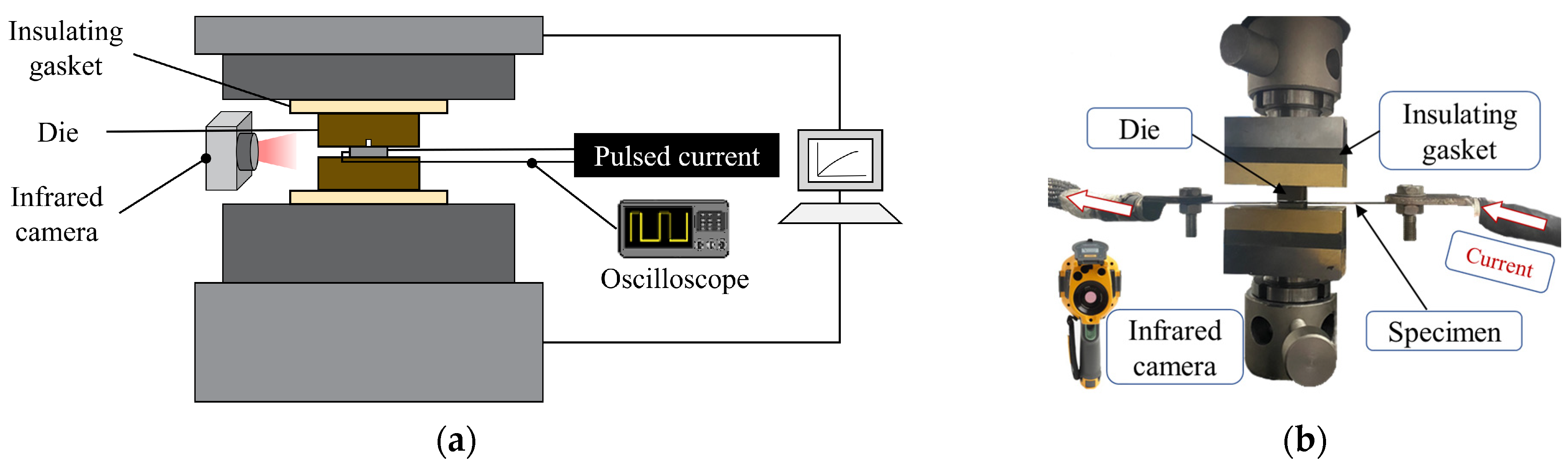
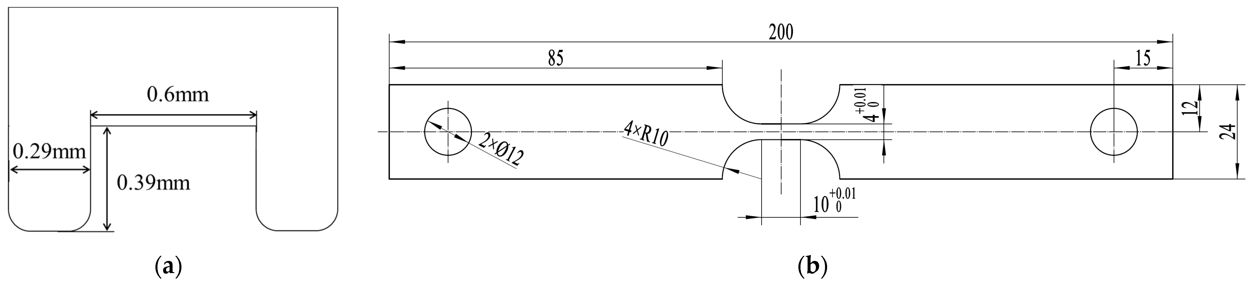
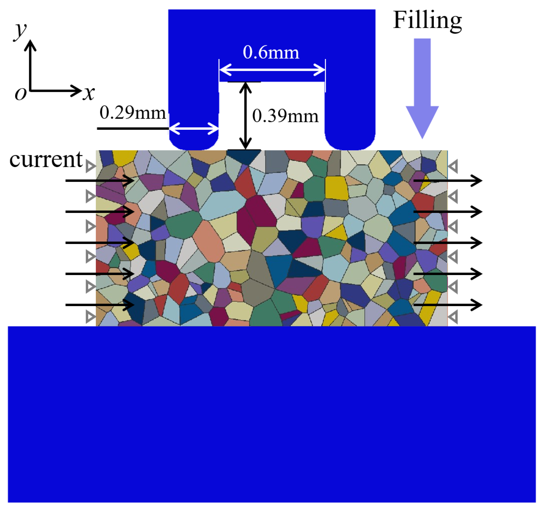
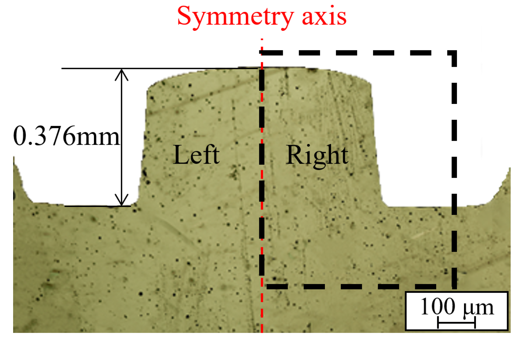
2.1. Electrically Assisted Micro-Filling Experiment

According to the electric field-assisted microforming experimental platform built by Meng et al. [21], the electrically assisted micro-filling experiments were conducted on SUS304 stainless steel, as shown in Figure 1. The die material is Cr12MoV, and the insulating material is the mica sheet. The real-time temperature of the specimen was monitored using the FLIR A615 infrared thermal imager during the filling process. The samples used for electrically assisted micro-filling were annealed at 1173 K in a vacuum furnace. First, the specimen was placed on the die and then energized. When the specimen temperature reached 700 °C due to the current, the punch started to move with the downward pressure of 6000 N. The filling process lasted about 1 min. After that, the shaped micro-channel morphology was observed and measured by electron microscope. Furthermore, the sample was cut by wire-cut electrical discharge machining, and the cross-section sample was prepared by electrolytic polishing. Then the electron backscatter diffraction (EBSD) was used to observe the microstructure of the filling specimen by Hikari XP EBSD probe, and the results were analyzed with OIM software. Forming quality is mainly measured by micro-channel morphology and structure size.
The main geometrical dimensions of the filling die in the electric field-assisted micro-filling experiment are shown in Figure 2a. The spacing of the micro-filling die is 0.6 mm, the tooth width is 0.29 mm, and the depth of the groove is 0.39 mm [21]. Figure 2b depicts the specimen of the micro-filling experiment. The left and right through-holes are convenient for connecting cables, and the current is directly input from one end of the workpiece and output from the other. In the experiment, the electricity was applied directly to the workpiece, making the specimen reach the required temperature faster and reducing heat loss. The narrow part in the middle is the area in contact with the punch, that is, the 4 mm machining area. The transition fillet of R10 on the specimen prevents stress concentration from causing a fracture at the root of the machining area.

2.2. Introduction of Electric Current in Constitutive Modeling

At present, researchers mainly focus on the thermal deformation of metal materials. However, the constitutive modeling of the electrically driven forming process is lacking [9,22]. Liu et al. [22] established the electro-assisted compression constitutive model of Ti6554 titanium alloy by modifying the Johnson-Cook model, whose parameters depend on current density. With the aid of Liu’s idea, it is noticed that the flow stress curves of samples under different current densities obey the empirical exponential function through the analysis of experimental data. The Voce equation [23] is used to characterize the flow stress:
σ ¯ = σ 0 + q ( 1 exp ( b ε ¯ p ) )
where σ ¯ is equivalent stress, ε ¯ p is the equivalent plastic strain, σ 0 is the initial yield stress, and q, b are material constants. Considering the influence of current density, σ 0 , q, and b in the Voce equation are represented as functions of current density:
σ 0 = m 0 + n 0 J q = m 1 + n 1 J + l 1 J 2 b = m 2 + n 2 J + l 2 J 2
where mi, ni, lj (i = 0,1,2; j = 1,2) are the material coefficients under the influence of current density J.
Focusing on the impact of grain size during pure copper micro-compression, Fu et al. [24] discovered that stress incompatibility vanishes at the grain boundary when plastic deformation occurs within grains. Thereby, it is possible to regard the grain interior and boundary as a separate portion, respectively. The flow stress can be obtained from the combined contribution of the grain core and boundary. Grain boundary has an adverse effect on dislocation slip within the grain, resulting in dislocation plugging. Only when the force of the dislocation source is greater than the critical stress of dislocation activation the dislocation slip occurs among grains. As a consequence, the flow stress of the grain boundary is believed to be greater than that of the grain interior. This research assumes that the plastic flow stress of the grain boundary is K times that of the grain core for convenience. For ease of description, grain interior is referred to as “GI”, and grain boundary is referred to as “GB”. Hence, the GI and GB stress can be represented as:
σ ( ε ) = F GI σ GI ( ε ) + F GB σ GB ( ε )
σ GB ( ε ) = K σ GI ( ε )
where FGI and FGB denote the GI and GB area fractions in two dimensions, respectively. σ GI ( ε ) and σ GB ( ε ) are the flow stress—strain relationship of GI and GB, respectively. K is constant, representing the stress relationship between the grain boundary and core.
The unequal distribution of grains with diverse sizes, constructions, and orientations in the material results in the dispersion effect of stress, which is regarded as the standard deviation of the mechanical flow curve [24]. The total GI flow stress consists of the contribution of each GI according to the ratio of area. Therefore, the grain area distribution is first obtained to calculate the probability density function (PDF), as shown in Figure 3a. Consequently, the statistical area distribution is normalized (Figure 3b) to generate the upper and lower limits as the range of GI properties. The flow stress-strain curves of each GI are obtained on the basis of the above PDF, as shown in Figure 3c.

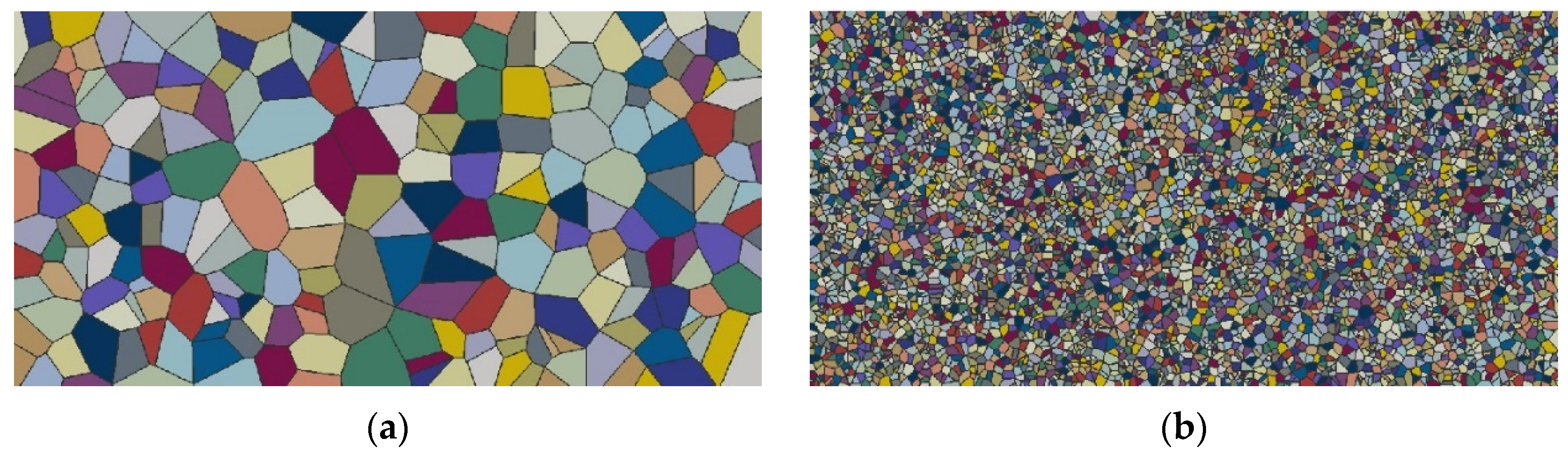
2.3. Finite Element Model of Electrically Assisted Micro-Filling

In the electrically assisted simulation process, the material properties are given in three aspects, including thermal, electrical, and mechanical. The mechanical characteristics of materials are mainly assigned through the above method in Section 2.2. For the setting of electrical parameters, the electrical conductivity of grain boundary with different grain sizes is the same but smaller than that of grain core [25]. The electrical conductivity of the grain boundary is set to be 0.8 times that of the grain interior, and the thermal parameters of GI and GB are identical, which are listed in Table 1. The die properties are shown in Table 2, where the electrical conductivity parameter is calculated by JMatPro [26].
Corresponding to the deformation region and the average grain size, two-dimensional crystal models of stainless steel with four μm quadrilateral mesh were established by NEPER [28]. The inp file output by NEPER was rewritten by MATLAB to generate the grain boundary combined with the common node method [29]. Next, it was loaded into ABAQUS to simulate the forming morphology and deformation behavior of samples with different grain sizes to analyze the influence of grain sizes on the forming performance in electrically assisted micro-filling forming.
According to the primary size of the micro-filling die as shown in Figure 2, the size of the crystal model is 2 mm × 1 mm considering the grain size and computational efficiency. The horizontal and vertical axis are the length and thickness direction of the stainless steel sheet, respectively, and the grain boundary thickness is approximately eight μm. As specified by the above description, different material properties are assigned to GI and GB, as shown in Figure 4. To probe the size effect of the electrically aided micro-filling process, the polycrystal models with the coarse grain (95 μm) and fine grain (18.81 μm) were established in Figure 5. Figure 6 shows the two-dimensional thermal–electrical–structural simulation model of micro-filling with an electric field. The current flows in from the left side of the model and discharges from the right side. Meanwhile, the symmetric constraint boundary conditions in the x direction are applied to the left and right sides of the crystal model. The micro-filling process is considered an isothermal forming process. Therefore, the thermoelectric coupling model was first established. After the specimen was powered up to 700 °C, the temperature field was transferred to the coupled thermo-mechanical model for the simulation of the filling process, where the displacement of the filling die was set to 0.4 mm.

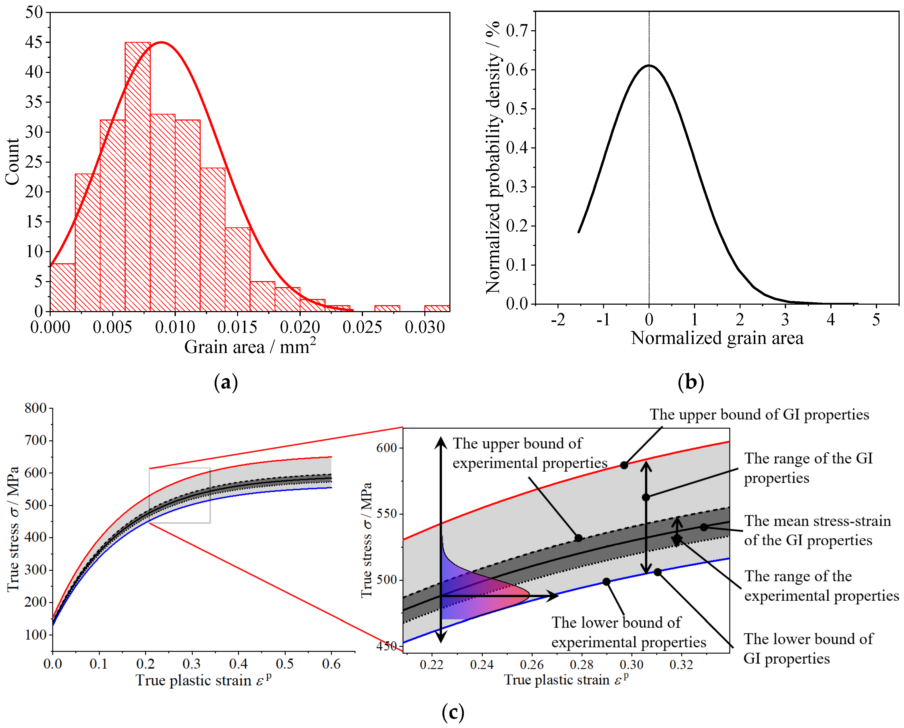
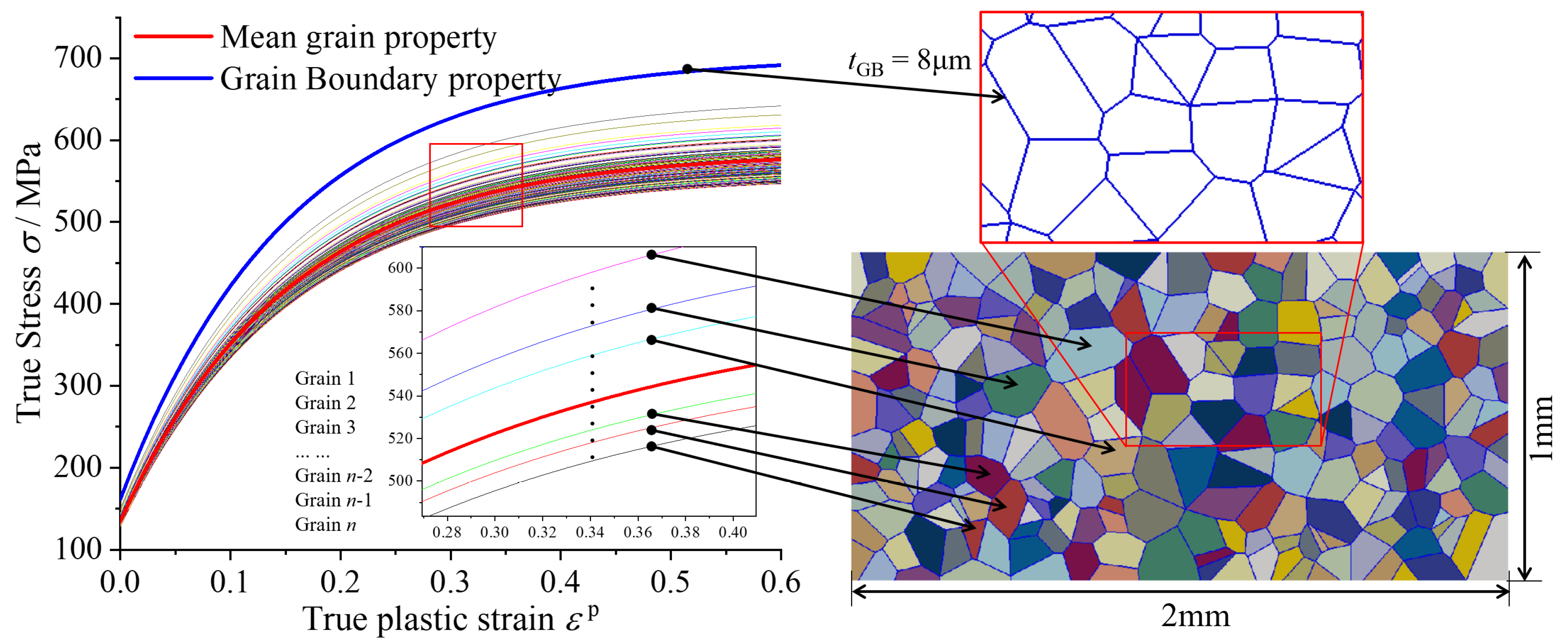
3. Results and Discussion

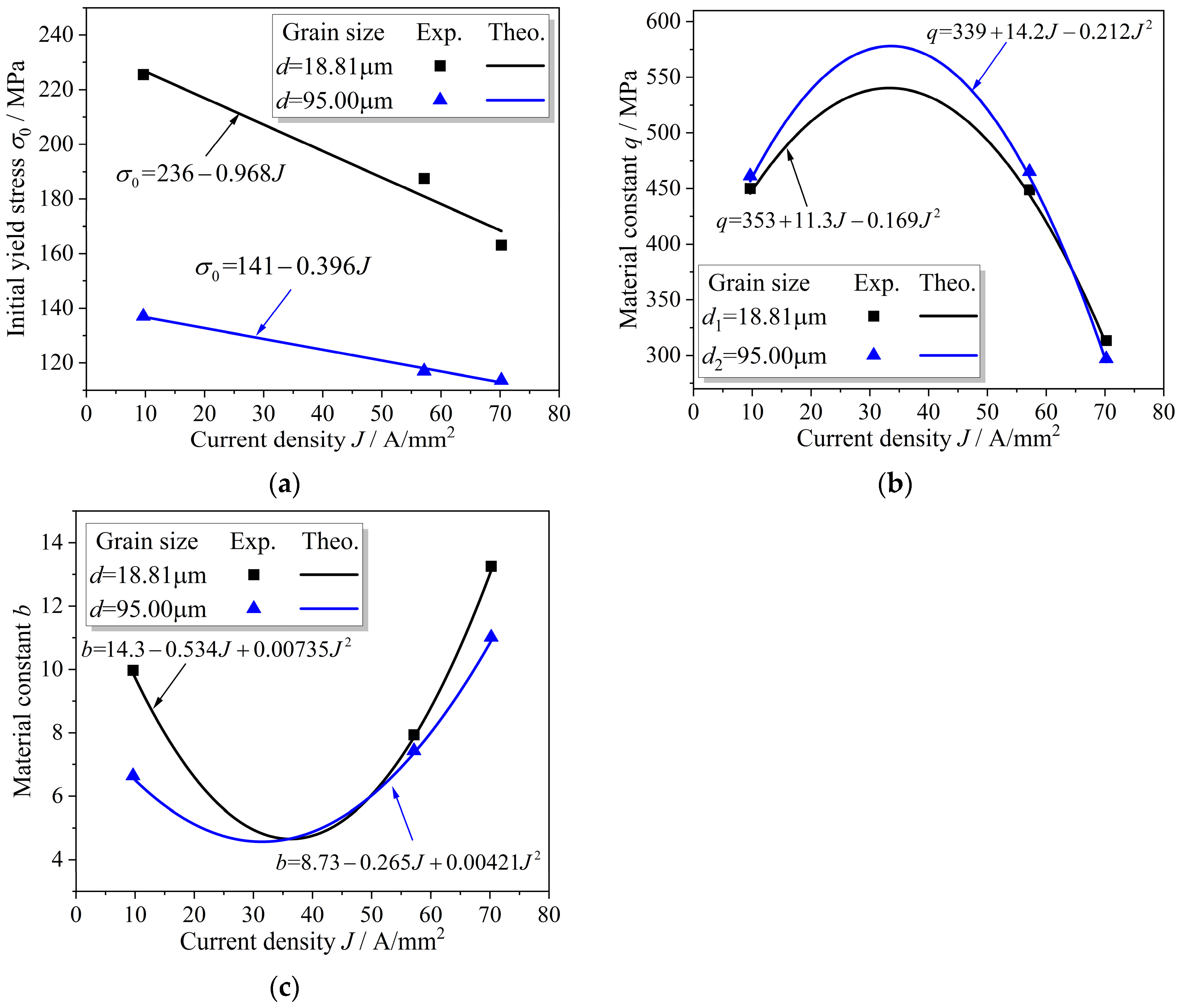
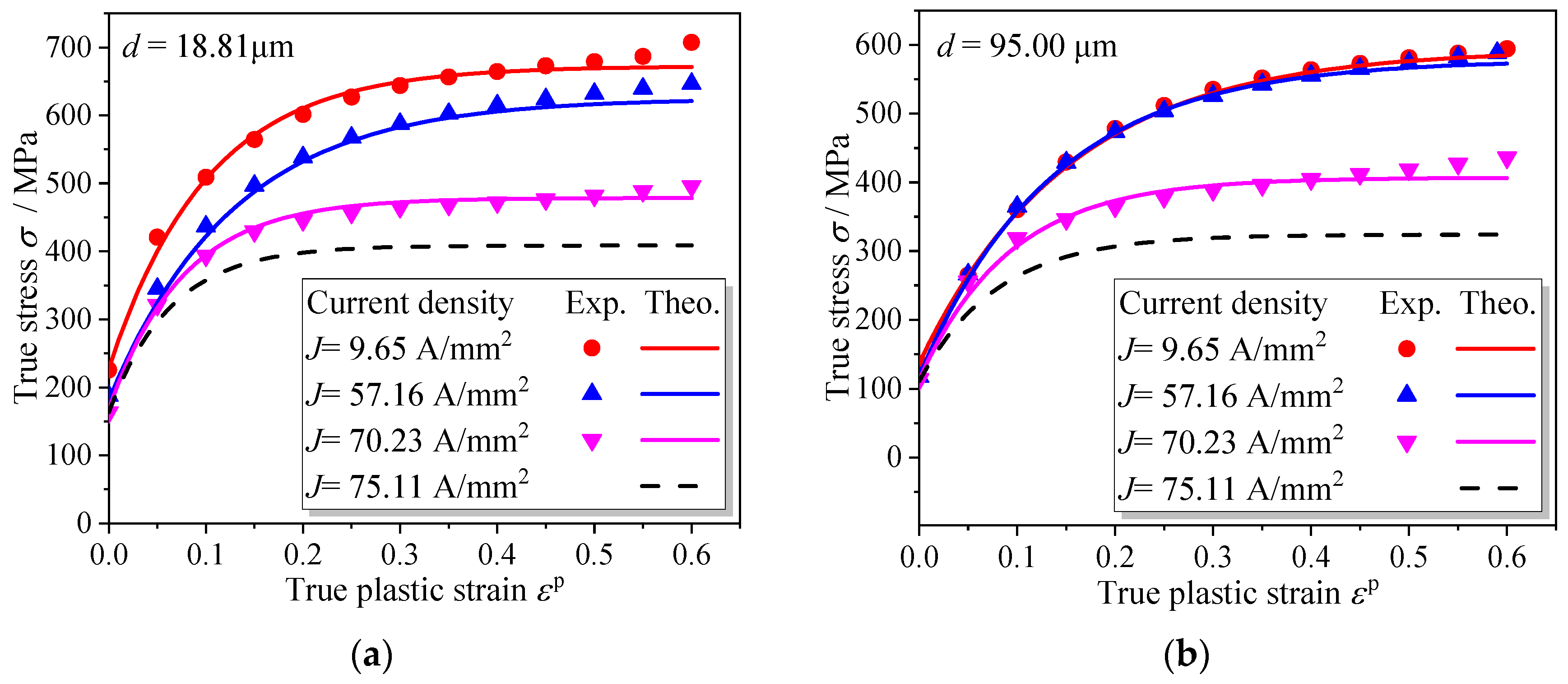
3.1. Constitutive Model Verification

The experimental data of electrically assisted micro-compression of SUS304 stainless steels are from Ref. [30]. The stainless steels with a grain size of 18.81 μm and 95 μm are chosen for model verification, and they are denoted as fine-grained (FG) and coarse-grained (CG) materials, respectively. The relationship between constitutive model parameters and current density is shown in Figure 7, where “Exp.” represents the experimental data and “Theo.” is the theoretical prediction value (the same below).
During the electrically assisted micro-compression experiment, the pulse power equipment could not make the temperature of the specimen reach 700 °C, even at a very high current density, and the temperature could not be kept stable at 700 °C. Therefore, the compression curves under 700 °C were not acquired by experiments but with the prediction method. After analyzing the experimental data, the relationship between current density and temperature can be expressed as an exponential function, as shown in Figure 8. As the electrical-assisted filling is performed at a temperature of 700 °C, it is predicted that the temperature can be up to 700 °C with a 75.11 A/mm2 current density through this relationship. In accordance with the above analysis and the established model, the compressive stress–strain curves with different current densities are predicted, as depicted in Figure 9. It is conspicuous that the established constitutive model can accurately describe the micro-compression curves with different grain sizes at the current density of 9.65, 57.16, and 70.23 A/mm2. Du et al. [30] pointed out that the micro-compression deformation of electric heating conforms to the law of the Hall–Petch equation. With the increase in current density, the flow stress exhibits a premature stable stage, and the stress–strain curves of CG and FG materials gradually converge. The predicted theoretical curve at 75.11 A/mm2 current density is consistent with the above rule. Therefore, the established constitutive model and prediction results are reasonable and practical.
It is challenging to determine the stress of grain boundary and grain interior through experiments. Their flow stresses are usually distributed by Equation (3) [31]. However, it is impossible to uniquely determine σ GI ε and σ GB ε with it. Fu et al. [32,33] assumed that the strength of the grain boundary is about 20% higher than that of the grain core. Although the material is copper, it still has a certain reference significance. Corresponding experiments are not carried out to determine the value of K in Equation (4) and verify it, so different K values are adopted for analysis.
As shown in Figure 10, multiple different relationships significantly affect the distribution of stress–strain curves. When K = 1.1, the maximum value of grain core flow stress is greater than that of grain boundary, which is not enough to distinguish between GB and GI, so it is considered unreasonable. When K = 1.3, although the stress of the grain boundary is higher than all grain interior curves, the diversity between GB and GI gradually increases with the increase in strain. Micro-filling is a large deformation process, and the significant difference between the two parts may lead to the non-convergence of finite element analysis. Figure 10c shows that the stress at the grain boundary is not only greater than the maximum value of the grain core when K = 1.2, but the difference is not as significant as when K = 1.3. Furthermore, the focus of this investigation is properties assignment, not the establishment of a constitutive model considering grain boundary. Based on the above analysis, it is reasonable to assign mechanical properties with K = 1.2, that is, σ GB ε = 1.2 σ GI ε .

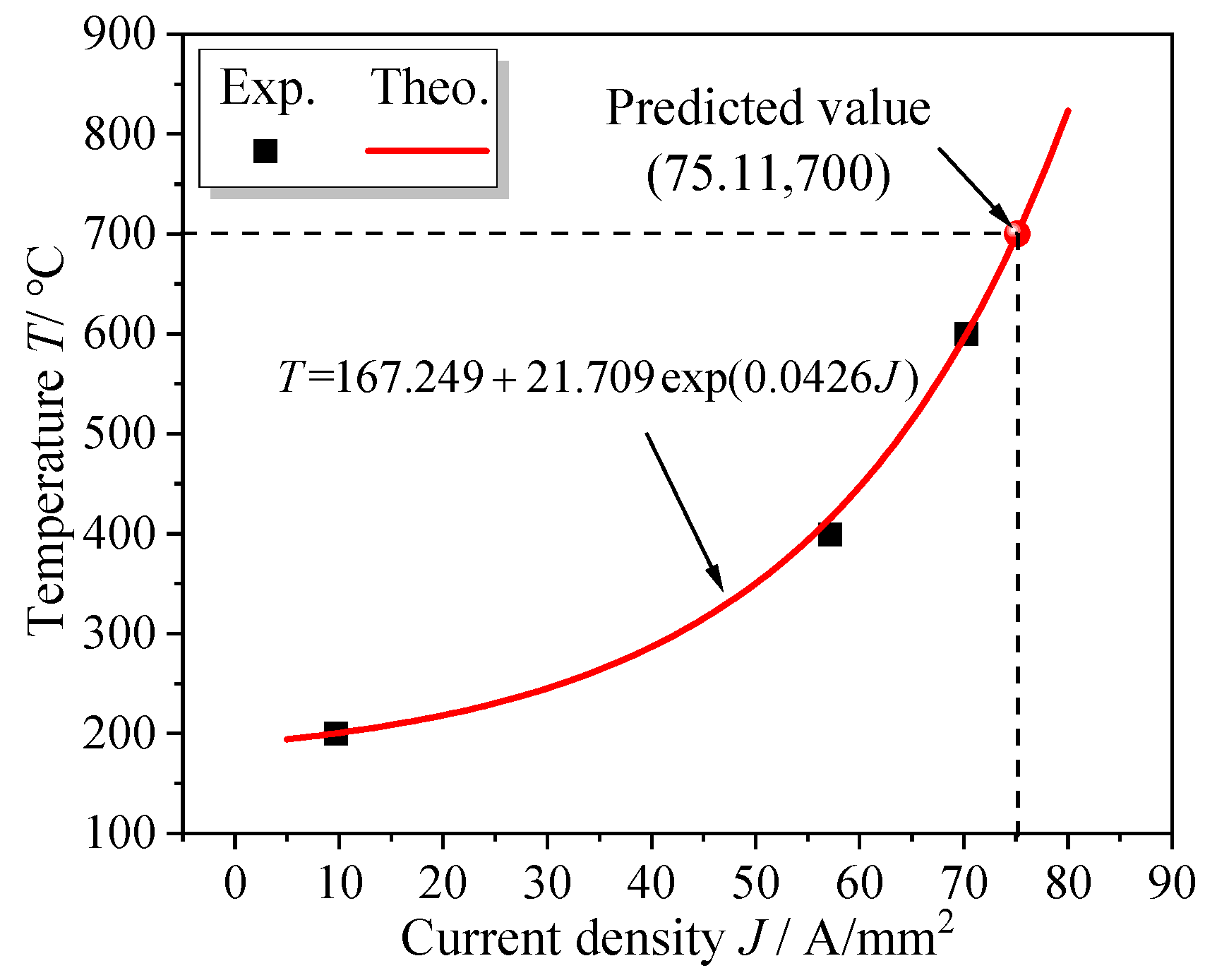
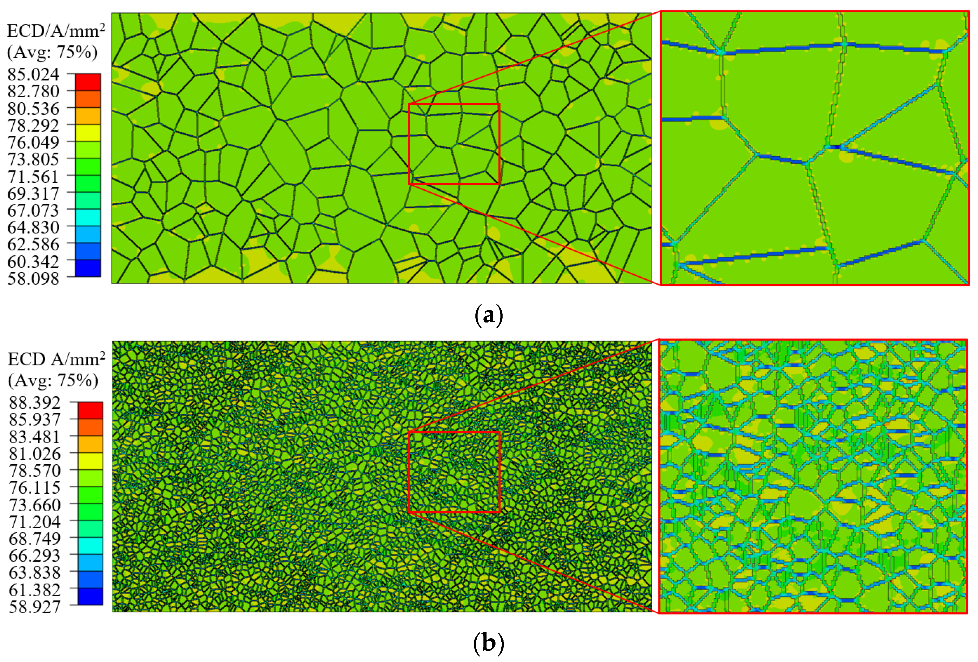
3.2. Effect of Grain Size on the Current Distribution

Figure 11 and Figure 12 show the temperature distribution of the die and specimens obtained by simulation, respectively. The experimental result indicates that the die temperature increases to about 80 °C due to heat exchange. Whereas the specimen surface temperature is about 700 °C during the filling process. The simulated temperature distribution of the die and the average temperature of the specimen surface is fairly coincident with the experimental counterparts.
As mentioned above, the micro-compression curves under 700 °C at a higher current density are not obtained, but the temperature of the specimen reaches 700 °C during the micro-filling, mainly because of the difference in the mode of electrification. As the compression samples are very small, it is difficult to directly energize the specimen. So the current is applied on the compression dies, which can be found in details from the work of Du et al. [30]. However, in the process of electrically assisted micro-filling, the current is directly applied to the deformed material. Therefore, the temperature of the filling specimen can reach 700 °C under a certain current density, but the micro-compression experiment cannot.
It is visible from Figure 12 that the deformation temperature increases with the decrease in grain size. The GB conductivity of materials with different grain sizes is the same but smaller than that of GI. In the same deformation area, the grain boundary density of the FG model is much higher than that of CG, resulting in a decrease in the overall conductivity of the FG material. In other words, the electrical resistivity of the FG sample is increased [34]. Consequently, the temperature of the FG model is 30~50 °C over that of the CG model at the same current density. It is consistent with the temperature difference between the CG and FG materials obtained by Du et al. [30] in the electrically assisted compression process. The rationality of the thermoelectric coupling model and the validity of the simulation results are further explained. In addition, both coarse and fine grains show a temperature gradient distribution from the center to the periphery.
There is no temperature gradient between the GI and GB under the action of current [25], but uneven electric current density (ECD) is observed at grain boundaries in the current density contour map, as shown in Figure 13, which is in accordance with the research results of Kim et al. [25]. However, for both CG and FG materials, the local heated areas are observed, and the temperature distribution is a gradient from the center to the periphery. In fact, the anisotropy of the materials is not considered in the finite element model but rather the difference in the physical properties at the grain boundary and core. The temperature distribution in Kim’s polycrystalline model [25] is relatively uniform after electrification, and there is no gradient difference, as shown in Figure 12. The electrical conductivity of the grain boundary is smaller than that of the grain interior, and there is heat exchange among the specimen, dies, and atmospheric environment. Therefore, the coupling effect of these factors leads to the ellipsoidal temperature distribution observed in Figure 12.

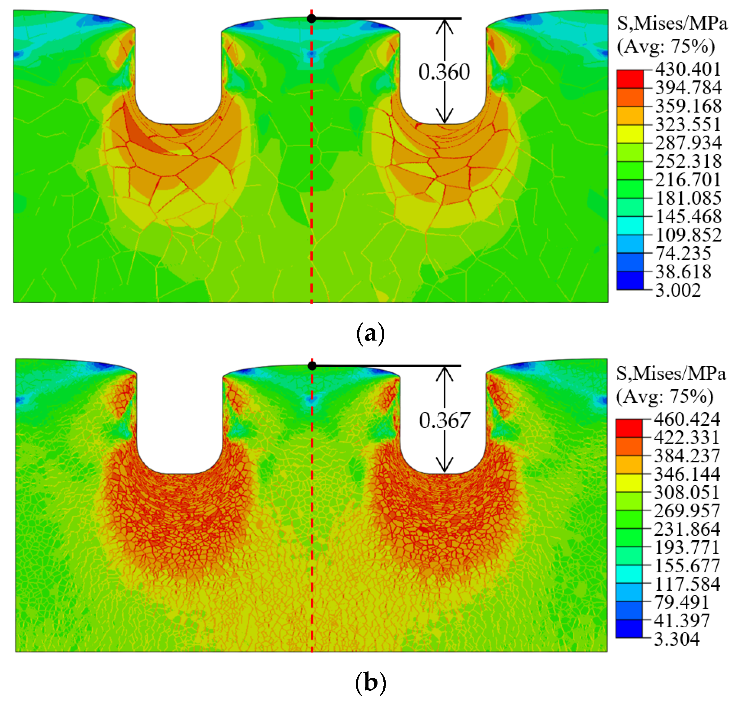
3.3. Effect of Grain Size on Micro-Filling Behavior

Figure 14 emerges the microfeature filling shape at the forming temperature of 700 °C. It is found that the left and right sides of the filling shape have good symmetry, and the slope of both sides of the microfeatures is slight. Although there is a radian at the top, the curvature is small, which is close to the designed shape. Moreover, the height of the highest point has reached 0.376 mm, indicating that the material has almost contacted the top of the cavity, while the punch displacement is 0.527 mm.
To explore the microstructure evolution of stainless steels sheet in the thickness direction with an electric field, the right region of the filling structure (the area in the black dotted box in Figure 14) was selected for EBSD tests, as shown in Figure 15a. Based on the grain morphology and orientation of different regions, three regions, A, B, and C, were extracted from the cross-section of the microfeature, as shown in Figure 15b–d.
It is noticeable from Figure 15 that the grain orientation in area A is dispersed because the grain is not directly affected by force, and the grain is large and massive, similar to the original grain. The grain in area B has the most severe deformation due to the large extrusion pressure, and the severe plastic deformation refines the grain size, showing a trend of flow into the die cavity. Although these grains are severely squeezed in area C, they are not refined into small grains except for a small part of the side wall. The material is softened, and the formability is improved under the action of the current. The grains are distributed in a strip shape along the deformation and filling direction.
It is illustrated in Figure 16 the comparison between the simulated microstructure and the experimental one after micro-filling. The left part shows the simulation result, and the experimental one is shown on the right. Similar to the experimental microstructure, the simulation result shows three regions labeled A’, B’, and C’. The variation of grain in the three regions reveals the same trend as the findings from experiments. In addition, the simulated micro-structure morphology has a good consistency with the experiment.
Figure 17 depicts the Mises stress distribution of fine- and coarse-grained samples after forming. When compared to the CG sample, the equivalent stress of the FG sample is shown to be roughly 30 MPa higher. In Figure 9, under the same temperature, the compressive stress in the FG material is 100 MPa greater than in the CG material. When the grain size decreases, the grain boundary density increases, and the grain boundary strengthening is boosted so that the deformation stress of the FG sample exceeds that of the CG one. In the simulation process of electric-assisted micro-filling, the FG sample’s temperature is comparatively higher, and the increase in the forming temperature reduces the deformation resistance of the micro-filling. In consequence, the flow stress of the FG sample is slightly larger.
Due to the difference in orientation of neighboring grains, it is difficult for the slip of dislocation to directly transition from one grain to another, and the deformation of each grain is inconsistent. To maintain the continuity of deformation, the deformation of neighboring grains must be coordinated. In Figure 17, it is evident that the filling height of the FG material is greater than that of the CG one, mainly because the grain size of the FG material is small. Under the same deformation amount, the FG sample has more grains to share the deformation resistance and participate in the slip deformation, leading to the strong ability of grain flow and coordination deformation. Additionally, the electroplastic effect induced by high-density current makes the material flow and fill into the die cavity more readily on account of the electroplastic effect brought on by high-density current [9]. In the CG sample, there are only about 5 grains along the horizontal direction of the die cavity, and fewer grains are involved in deformation. The deformation shared by each grain is considerable, which makes the single grain seriously distorted. Grain interior and grain boundary have extremely distinct deformation, and it is difficult to coordinate with each other in view of the deformation among grains, leading to increased deformation unevenness. The grain flow of CG material is tougher than that of FG material, which increases the difficulty of micro-filling forming. The nonuniformity of this coordination becomes more obvious with the increase in deformation. Hence, the radian is great at the top of the filling microfeature but not as flat as the top of the FG sample.

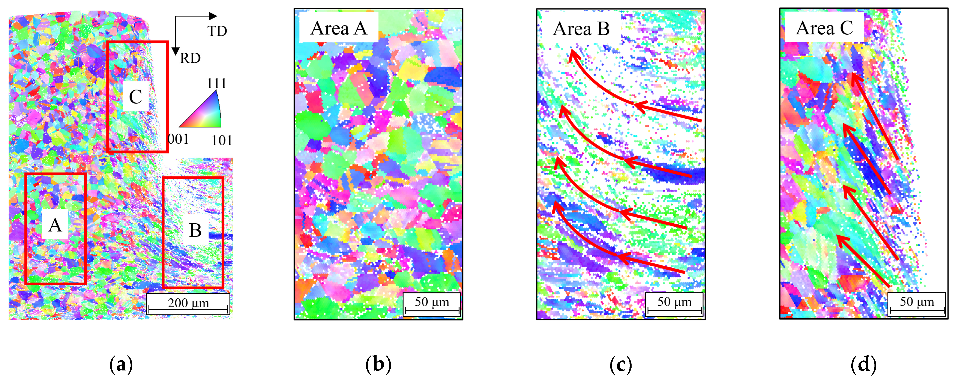
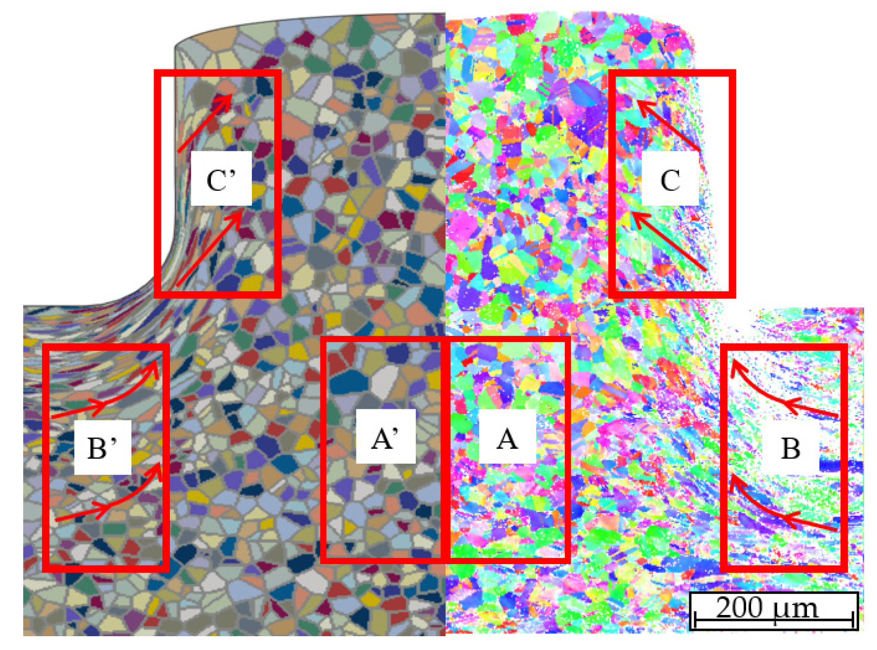
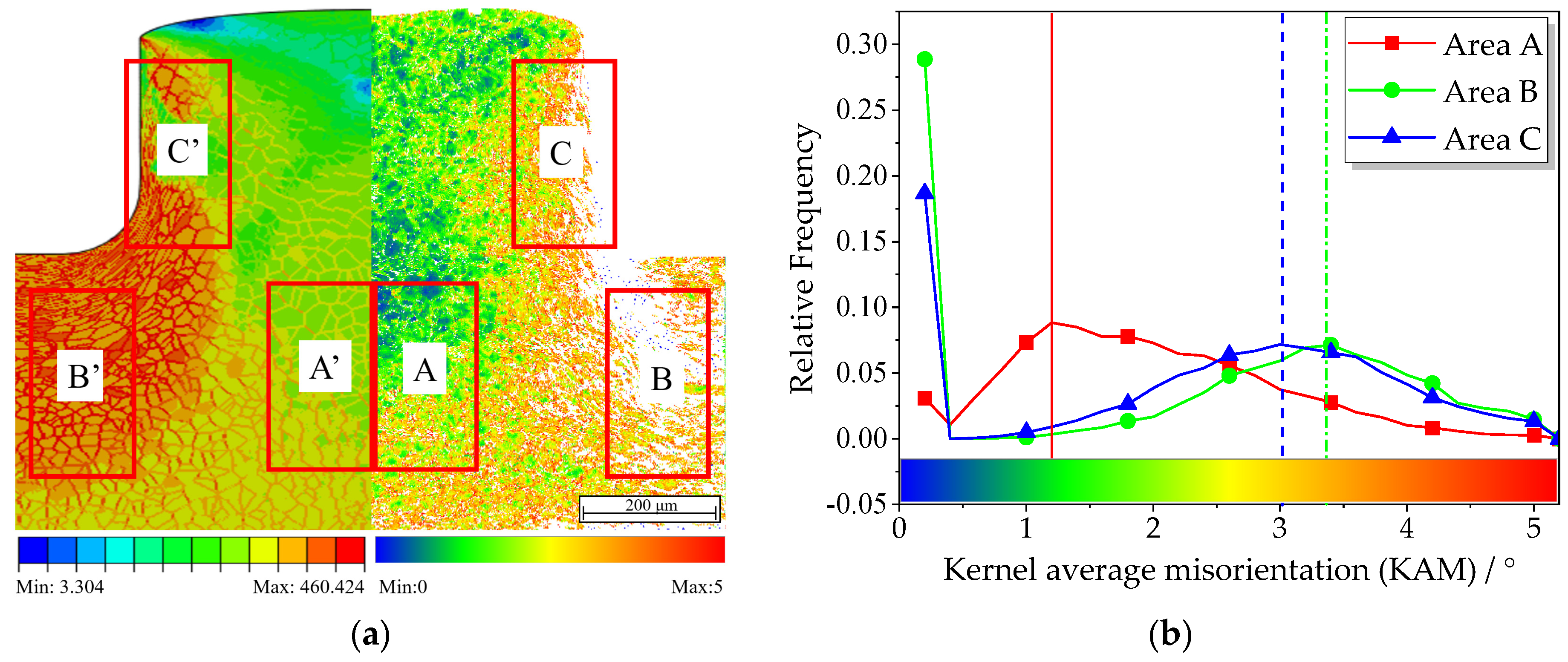
3.4. Microscopic Response under Electric Current

In tandem with the above outcomes, it is proved that the reduction of grain size and the electric field-assisted deformation are helpful to the filling forming of micro features. As can be seen from Figure 16, the trend of stress distribution is consistent in both coarse and fine grains, and a large stress concentration exists near the grain boundary. Especially at the bottom of the filling structure, namely, the protrusion part of the filling die, the stress concentration is apparent. Kernel average misorientation (KAM) is usually used to characterize the dislocation density of materials [35] to assess the state of stress distribution in the deformation process. KAM is proportional to the geometric dislocation density [36]. Therefore, to explore the dislocation evolution and stress distribution in different regions, the KAM distributions of the whole and areas A, B, and C are output, as shown in Figure 18. Here, areas A – C and A’ – C’ are different deformation regions which are the same as in Figure 16.
According to the corresponding relationship between the simulated stress distribution (Figure 17) and the KAM distribution (Figure 18), the stress concentration occurs where the KAM value is enormous. The higher grain boundary density of the FG sample resulting in more serious dislocation plugging, and the stress concentration phenomenon is more apparent. The extensive recrystallization nucleation position and powerful energy storage capacity at the grain boundary of FG material are the reason why the FG sample recrystallizes at a higher pace than the CG sample. More dislocation is consumed at the grain boundary of the FG sample by the recrystallization nucleation. The electric current can stimulate recrystallization nucleation and consume dislocations, thus alleviating strain hardening and reducing deformation resistance. Moreover, the current can shrink the difference in microstructure evolution between CG and FG samples and the size effect of the mechanical behavior of materials [30]. Therefore, the deformation resistance of CG and FG samples and the difference in filling microfeatures are reduced.
It is noteworthy from Figure 18 that the KAM value in region A is relatively low, and the dislocation density value is small. Based on Figure 16 and Figure 17, it can be found that there is almost no grain deformation in area A, which is well confirmed by the simulation results (area A in Figure 18a). The KAM value of area C is lower than that of area B. Although area C is also affected by deformation, the deformation degree is not as severe as that of region B. Figure 18a reveals that there is a certain stress concentration in the corresponding area C’, but the concentration level is not as high as that in area B’. The deformation in area B is the most severe, and the KAM value corresponding to the peak value in this region is the largest, indicating a high dislocation density. In the process of electric-assisted micro-filling, the extrusion of area B resulted in very great deformation and material strengthening, which is essential because the grain boundary impeded the dislocation movement. The dislocation moves to the grain boundary and accumulates gradually, causing stress concentration at the grain boundary. With the accumulation of the dislocation, the stress concentration at the grain boundary increases, as shown in Figure 17b. Although the current can reduce the dislocation density and alleviate the dislocation plugging at the grain boundary [30], the structure and energy of the grain boundary do not change substantially during the process. As a result, there is still a large stress concentration.

4. Conclusions

In this research, the constitutive model of electrically assisted deformation and electrical–thermal–structural coupling polycrystal model was established for the finite element simulation of electrical-assisted micro-filling of SUS304 stainless steel. The simulated results are compared with the experimental findings. The main conclusions are drawn as follows:
(1)
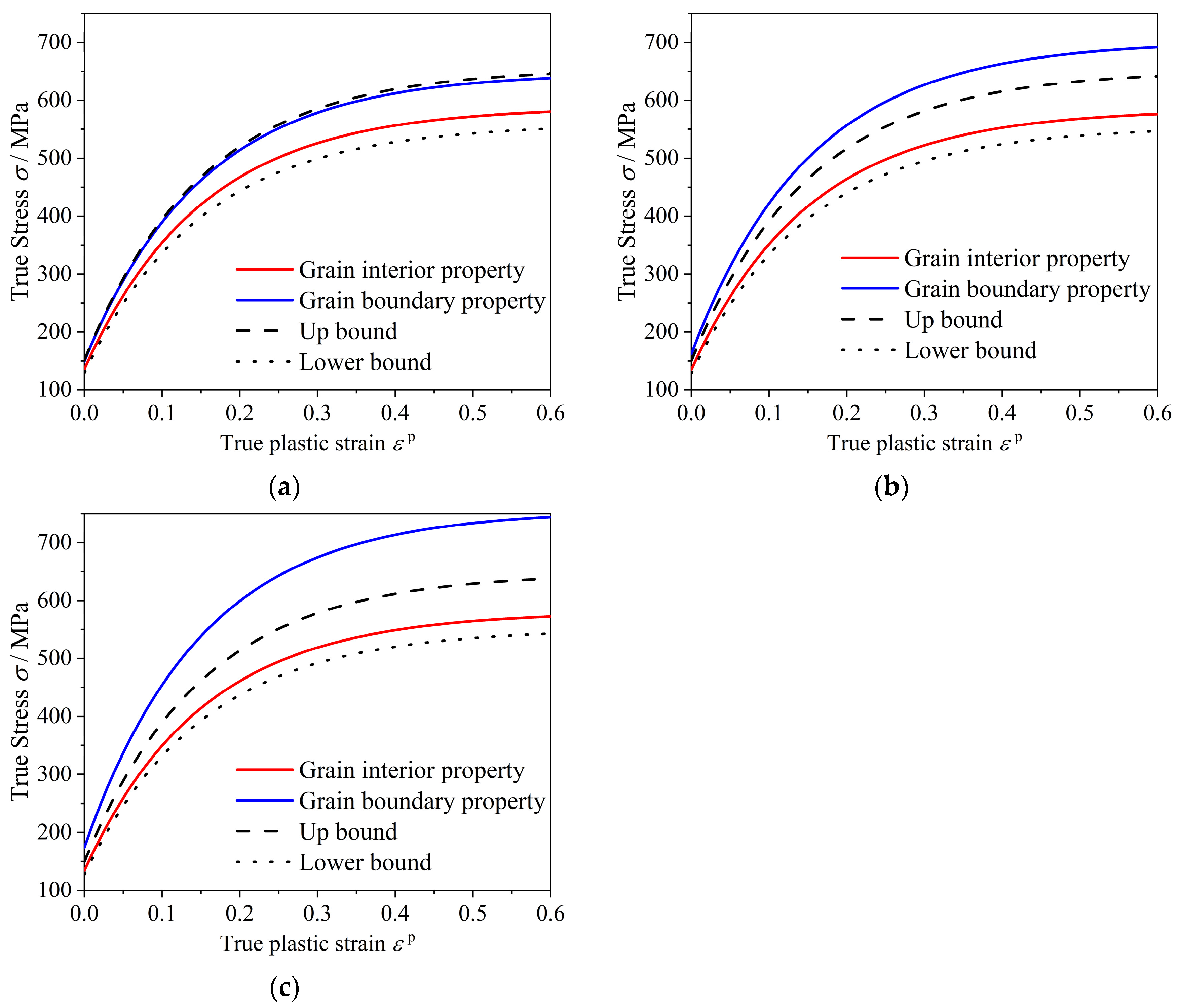
The established constitutive model considering electric current can better predict the compression flow behavior of SUS304 stainless steel under different current densities. The distribution of mechanical and physical properties of grain boundary and grain interior is reasonable.
(2)
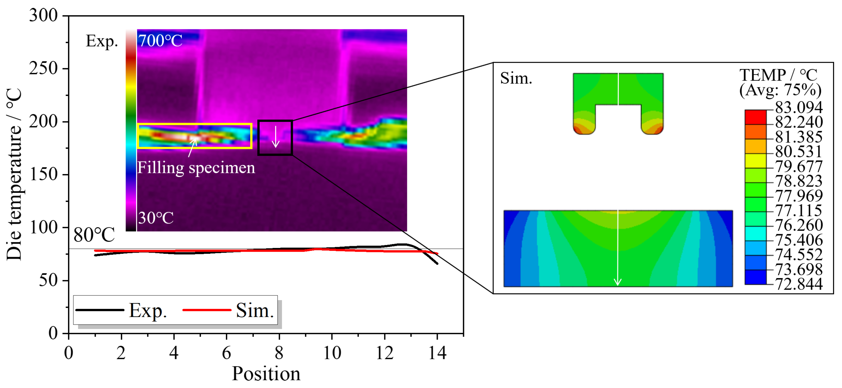
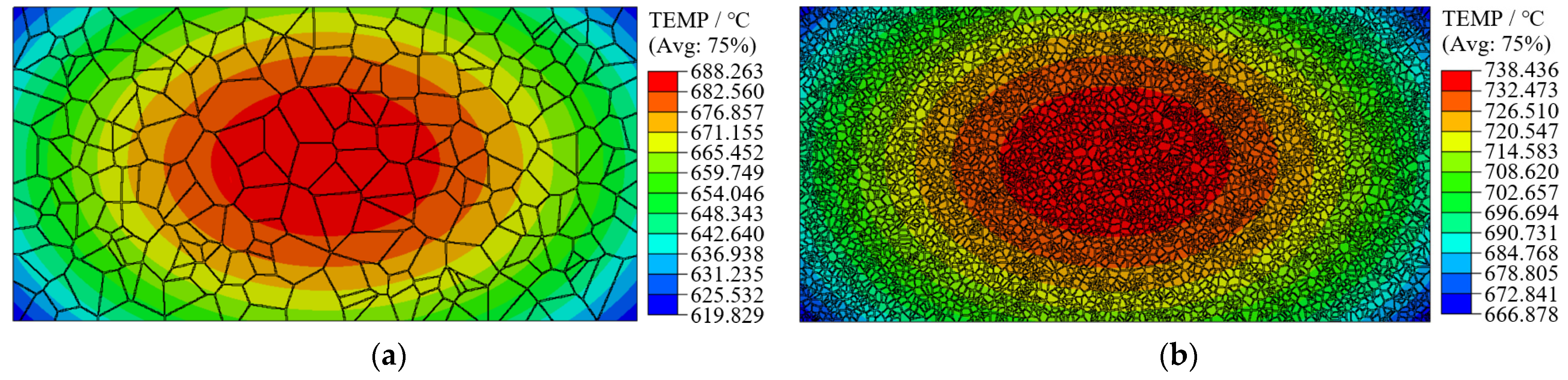
Under the action of the current, the non-uniform current density is observed between the grain interior and grain boundary, but there is no local joule heat. Under the same current density, the increase in grain boundary density makes the resistivity of the fine-grained material more considerable, and the temperature of the specimen increases with the decrease in grain size. In addition, the temperature of the specimen presents a gradient distribution from the center to the periphery.
(3)
The coordination among grains of fine-grained materials is stronger than that of coarse-grained counterparts. The reduction of grain size and the electrically assisted deformation are helpful to the micro-filling forming of microfeatures, resulting in better quality and higher feature height. The deformation and flow of grains in different regions and the surface temperature difference in specimens obtained from the finite element analysis are in good agreement with the experimental results, which proves the validity of the established electrical–thermal–structural coupling polycrystal model.
(4)
Due to the fact of higher grain boundary density of the fine-grained sample, the dislocation plugging is more serious, causing obvious and great stress concentration. The difference in microstructure evolution and mechanical behavior between coarse-grained and fine-grained samples is reduced by the introduction of electric current, and the difference in deformation resistance and filling microfeatures between coarse-grained and fine-grained samples is abated.

Author Contributions

Conceptualization, B.M.; methodology, M.M.; software, Y. L.; validation, R.Z.; formal analysis, M.W.; investigation, M.M. and Y.L.; resources, B.M. and R.Z.; data curation, B.M.; writing—original draft preparation, M.M.; writing—review and editing, B.M.; visualization, M.M.; supervision, M.W.; project administration, B.M.; funding acquisition, B.M. All authors have read and agreed to the published version of the manuscript.

Funding

This research was supported by the Foundation of Basic Research Strengthening Plan of China, grant number 2019JCJQ-JJ-257, and National Natural Science Foundation of China, grant number 52105316.

Data Availability Statement

Not applicable.

Acknowledgments

The authors would like to acknowledge the financial support by the Foundation of Basic Research Strengthening Plan of China with grant number 2019JCJQ-JJ-257, National Natural Science Foundation of China with grant number 52105316, and Jiangxi Research Institute of Beihang University.

Conflicts of Interest

On behalf of all authors, the corresponding author states that there is no conflict of interest.

References

  1. Meng, B.; Wan, M.; Zhao, R.; Zou, Z.; Liu, H. Micromanufacturing technologies of compact heat exchangers for hypersonic precooled airbreathing propulsion: A review. Chin. J. Aeronaut. 2021, 34, 79–103. [Google Scholar] [CrossRef]
  2. Shi, J.J.; Meng, B.; Cheng, C.; Wan, M. Size Effect on the Subsequent Yield and Hardening Behavior of Metal Foil. Int. J. Mech. Sci. 2020, 180, 105686. [Google Scholar] [CrossRef]
  3. Gao, Z.; Peng, L.; Yi, P.; Lai, X. Grain and geometry size effects on plastic deformation in roll-to-plate micro/meso-imprinting process. J. Mater. Process. Technol. 2015, 219, 28–41. [Google Scholar] [CrossRef]
  4. Xing, G. Research on Micro-Embossing Process in Ultrafine-Grained AZ31 Mg Alloy. Master’s Thesis, Harbin Institute of Technology, Harbin, China, 2017. (In Chinese). [Google Scholar]
  5. Li, J. Research on the Mechanism of the Micro-Forming and Filling Behavior of Ultrafine-Grained Pure Copper. Ph.D. Thesis, Harbin Institute of Technology, Harbin, China, 2018. (In Chinese). [Google Scholar]
  6. Qiao, X.G.; Gao, N.; Moktadir, Z.; Kraft, M.; Starink, M.J. Fabrication of MEMS components using ultrafine-grained aluminium alloys. J. Micromech. Microeng. 2010, 20, 045029. [Google Scholar] [CrossRef] [Green Version]
  7. Kim, G.-Y.; Koç, M.; Ni, J. Experimental and numerical investigations on microcoining of stainless steel 304. J. Manuf. Sci. Eng. 2008, 130, 041017. [Google Scholar] [CrossRef]
  8. Yao, Z.; Kim, G.-Y.; Faidley, L.; Zou, Q.; Mei, D.; Chen, Z. Effects of superimposed high-frequency vibration on deformation of aluminum in micro/meso-scale upsetting. J. Mater. Process. Technol. 2012, 212, 640–646. [Google Scholar] [CrossRef]
  9. Peng, L.; Mai, J.; Jiang, T.; Lai, X.; Lin, Z. Experimental investigation of tensile properties of SS316L and fabrication of micro/mesochannel features by electrical-assisted embossing process. J. Micro Nano-Manuf. 2014, 2, 021002. [Google Scholar] [CrossRef]
  10. Xu, J.; Xing, G.; Shan, D.; Guo, B.; Langdon, T.G. An evaluation of formability using micro-embossing on an ultrafine-grained magnesium AZ31 alloy processed by high-pressure torsion. In Proceedings of the 4th International Conference on New Forming Technology, Scotland, UK, 6–9 August 2015. [Google Scholar] [CrossRef] [Green Version]
  11. Xu, J.; Su, Q.; Wang, C.; Wang, X.; Shan, D.; Guo, B.; Langdon, T.G. Micro-embossing formability of a superlight dual-phase Mg–Li alloy processed by high-pressure torsion. Adv. Eng. Mater. 2019, 21, 1800961. [Google Scholar] [CrossRef] [Green Version]
  12. Su, Q.; Xu, J.; Wang, C.; Shan, D.; Guo, B. The fabrication of micro-array channels with the ultrafine-grained LZ91 Mg-Li alloy by micro-embossing. Micromachines 2018, 9, 55. [Google Scholar] [CrossRef]
  13. Xu, J.; Su, Q.; Shan, D.; Guo, B. Sustainable micro-manufacturing of superhydrophobic surface on ultrafine-grained pure aluminum substrate combining micro-embossing and surface modification. J. Clean. Prod. 2019, 232, 705–712. [Google Scholar] [CrossRef]
  14. Xu, J.; Shi, L.; Wang, C.; Shan, D.; Guo, B. Micro hot embossing of micro-array channels in ultrafine-grained pure aluminum using a silicon die. J. Mater. Process. Technol. 2015, 225, 375–384. [Google Scholar] [CrossRef]
  15. Su, Q.; Xu, J.; Yu, H.; Shi, L.; Shan, D.; Guo, B. Effect of grain size on formability and deformation mechanism of high-purity aluminum during micro-embossing process at elevated temperature. Adv. Eng. Mater. 2019, 21, 1900690. [Google Scholar] [CrossRef]
  16. Mai, J.; Peng, L.; Lai, X.; Lin, Z. Electrical-assisted embossing process for fabrication of micro-channels on 316L stainless steel plate. J. Mater. Process. Technol. 2013, 213, 314–321. [Google Scholar] [CrossRef]
  17. Mai, J. Simulation and Experiment Study on Electric Assisted Embossing Process of Stainless Steel 316L. Ph.D. Thesis, Shanghai Jiao Tong University, Shanghai, China, 2014. (In Chinese). [Google Scholar]
  18. Qiao, X.G.; Bah, M.T.; Zhang, J.; Gao, N.; Moktadir, Z.; Kraft, M.; Starink, M.J. Microembossing of ultrafine grained Al: Microstructural analysis and finite element modelling. J. Micromechanics Microengineering 2010, 20, 105002. [Google Scholar] [CrossRef] [Green Version]
  19. Wang, C. Research on Micro-Embossing Process in Ultrafine-Grained LZ91 Mg-Li Alloy. Master’s Thesis, Harbin Institute of Technology, Harbin, China, 2016. (In Chinese). [Google Scholar]
  20. Wang, C.; Wang, C.; Xu, J.; Zhang, P.; Shan, D.; Guo, B. Interactive effect of microstructure and cavity dimension on filling behavior in micro coining of pure nickel. Sci. Rep. 2016, 6, 23895. [Google Scholar] [CrossRef] [PubMed] [Green Version]
  21. Meng, B.; Pan, F.; Du, M.; Wan, M. Research on arrayed micro-channel electric field assisted roll forming technology. J. Mech. Eng. 2022, 58, 231–241. (In Chinese) [Google Scholar]
  22. Liu, B.; Wu, C.; Zhou, Y. Establishment and application of Ti6554 titanium alloy pulse current assisted compression constitutive model. J. Netshape Form. Eng. 2022, 14, 27–35. (In Chinese) [Google Scholar]
  23. Wang, H.; Men, M.; Yan, Y.; Wan, M.; Li, Q. Prediction of Eight Earings in Deep Drawing of 5754O Aluminum Alloy Sheet. Chin. J. Mech. Eng. 2019, 32, 146–154. [Google Scholar] [CrossRef] [Green Version]
  24. Chan, W.L.; Fu, M.W.; Lu, J.; Liu, J.G. Modeling of grain size effect on micro deformation behavior in micro-forming of pure copper. Mater. Sci. Eng. A 2010, 527, 6638–6648. [Google Scholar] [CrossRef]
  25. Kim, M.-J.; Yoon, S.; Park, S.; Jeong, H.-J.; Park, J.-W.; Kim, K.; Jo, J.; Heo, T.; Hong, S.-T.; Cho, S.H.; et al. Elucidating the origin of electroplasticity in metallic materials. Appl. Mater. Today 2020, 21, 100874. [Google Scholar] [CrossRef]
  26. Liu, Y.Z.; Wan, M.; Meng, B. Multiscale modeling of coupling mechanisms in electrically assisted deformation of ultrathin sheets: An example on a nickel-based superalloy. Int. J. Mach. Tools Manuf. 2021, 162, 103689. [Google Scholar] [CrossRef]
  27. Liu, Y. Morphology Prediction and Numerical Simulation of Laser Cladding Nickel-Based Alloy Coating on Cr12MoV Steel; Chongqing University of Technology: Chongqing, China, 2022. (In Chinese) [Google Scholar]
  28. Quey, R.; Dawson, P.R.; Barbe, F. Large-scale 3D random polycrystals for the finite element method: Generation, meshing and remeshing. Comput. Methods Appl. Mech. Eng. 2011, 200, 1729–1745. [Google Scholar] [CrossRef] [Green Version]
  29. Li, H.; Sun, X.; Zhan, M.; Huang, D. Microstructure based 3D finite element modeling methods of polycrystalline materials. J. Plast. Eng. 2020, 27, 6–12. (In Chinese) [Google Scholar]
  30. Du, M.; Meng, B.; Liu, Y.Z.; Pan, F.; Wan, M. Flow characteristics and microstructural evolution in pulsed current assisted micro-scaled compression of stainless steel sheet. J. Mater. Res. Technol. 2021, 15, 4397–4414. [Google Scholar] [CrossRef]
  31. Jiang, Z.; Zhao, J.; Xie, H. Chapter 6—Simulation Models in Microforming. In Microforming Technology; Jiang, Z., Zhao, J., Xie, H., Eds.; Academic Press: Cambridge, MA, USA, 2017; pp. 111–130. [Google Scholar]
  32. Li, W.T.; Fu, M.W.; Shi, S.Q. Study of deformation and ductile fracture behaviors in micro-scale deformation using a combined surface layer and grain boundary strengthening model. Int. J. Mech. Sci. 2017, 131–132, 924–937. [Google Scholar] [CrossRef]
  33. Chan, W.L.; Fu, M.W. Experimental studies and numerical modeling of the specimen and grain size effects on the flow stress of sheet metal in microforming. Mater. Sci. Eng. A 2011, 528, 7674–7683. [Google Scholar] [CrossRef]
  34. Salandro, W.A.; Jones, J.J.; Bunget, C.; Mears, L.; Roth, J.T. Electrically Assisted Forming: Modeling and Control; Springer: Cham, Switzerland, 2014; pp. 37–54. [Google Scholar]
  35. Wright, S.I.; Nowell, M.M.; Field, D.P. A review of strain analysis using electron backscatter diffraction. Microsc. Microanal. 2011, 17, 316–329. [Google Scholar] [CrossRef]
  36. Calcagnotto, M.; Ponge, D.; Demir, E.; Raabe, D. Orientation gradients and geometrically necessary dislocations in ultrafine grained dual-phase steels studied by 2D and 3D EBSD. Mater. Sci. Eng. A 2010, 527, 2738–2746. [Google Scholar] [CrossRef]
Figure 1. Electrically assisted micro-filling experiment platform: (a) Schematic diagram; (b) Physical installation.
Crystals 13 00134 g001
Figure 2. Die and specimen design of micro-filling experiment (Unit: mm): (a) Filling die; (b) Specimen.
Crystals 13 00134 g002
Figure 3. The process of generating GI stress-strain curves: (a) GI area distribution; (b) Normalized distribution; (c) Upper and lower limits of GI.
Crystals 13 00134 g003
Figure 4. Macroscopic size and properties assignment of polycrystal model.
Crystals 13 00134 g004
Figure 5. Polycrystal models of SUS304 stainless steel with different grain sizes: (a) 95 μm; (b) 18.81 μm.
Crystals 13 00134 g005
Figure 6. Two-dimensional simulation finite element model of electrically assisted micro-filling.
Crystals 13 00134 g006
Figure 7. Relation between material parameters and current density: (a) The initial yield stress σ 0 ; (b) Material constant q; (c) Material constant b.
Crystals 13 00134 g007
Figure 8. Relationship between temperature and current density.
Crystals 13 00134 g008
Figure 9. Experimental and theoretical prediction of true stress–true plastic strain curves of electro-assisted micro-compression under different grain sizes and current densities: (a) 18.81 μm; (b) 95 μm.
Crystals 13 00134 g009
Figure 10. Distribution of mechanical properties about grain boundary and grain interior at 9.65 A/mm2 with 95 μm: (a) K = 1.1; (b) K = 1.2; (c) K = 1.3.
Crystals 13 00134 g010
Figure 11. Comparison between simulated temperature distribution and experimental results.
Crystals 13 00134 g011
Figure 12. Distribution of temperature in polycrystalline under application of electric current in finite element analysis: (a) CG model; (b) FG model.
Crystals 13 00134 g012
Figure 13. Distribution of ECD in polycrystalline under the electric current application in finite element analysis: (a) CG model; (b) FG model.
Crystals 13 00134 g013
Figure 14. A cross-section view of a filling microfeature.
Crystals 13 00134 g014
Figure 15. Microstructures of different regions: (a) Right region; (b) Area A; (c) Area B; (d) Area C.
Crystals 13 00134 g015
Figure 16. Comparison of microstructure between simulation (left) and experiment (right).
Crystals 13 00134 g016
Figure 17. Mises stress distribution and filling height after micro-filling simulation: (a) CG model; (b) FG model.
Crystals 13 00134 g017
Figure 18. KAM distributions (2nd nearest-neighbor): (a) Global; (Here, blue and red color indicate the minimum value and maximum value, respectively); (b) Three areas.
Crystals 13 00134 g018
Table 1. Electrical and thermal properties of SUS304 [26].
Temperature (°C)Thermal Conductivity (W/m·°C)Specific Heat Capacity (J/Kg·°C)Density (kg/m3)Coefficient of Thermal
Expansion (×10−5)
Electrical Conductivity (S/m)
GIGB
014.646278101.701,436,7811,149,425.8
10015.14961.741,287,0011,029,601.8
20016.15121.801,177,856942,284.8
30017.95251.861,092,896874,316.8
40018.05401.911,024,590819,672.0
60020.85771.96931,099744,879.2
80023.96042.02870,322696,257.6
Table 2. Electrical and thermal properties of Cr12MoV [27].
Temperature (°C)Thermal Conductivity (W/m·°C)Specific Heat Capacity (J/Kg·°C)Density (kg/m3)Coefficient of Thermal
Expansion (×10−5)
Electrical Conductivity (S/m)
2034.0346078501.61946,800,000
27,900,000
17,300,000
7,600,000
20035.745301.693
40034.876202.323
80027.218202.389
Disclaimer/Publisher’s Note: The statements, opinions and data contained in all publications are solely those of the individual author(s) and contributor(s) and not of MDPI and/or the editor(s). MDPI and/or the editor(s) disclaim responsibility for any injury to people or property resulting from any ideas, methods, instructions or products referred to in the content.

