Article

Enhancement Mode Ga2O3 Field Effect Transistor with Local Thinning Channel Layer

1
The Institute of Novel Semiconductors, Shandong University, Jinan 250100, China
2
The Shandong Technology Center of Nanodevices and Integration, School of Microelectronics, Shandong University, Jinan 250100, China
3
The State Key Laboratory of Crystal Materials, Shandong University, Jinan 250100, China
4
The School of Electrical and Electronic Engineering, The University of Manchester, Manchester M13 9PL, UK
*
Authors to whom correspondence should be addressed.
Crystals 2022, 12(7), 897; https://doi.org/10.3390/cryst12070897
Submission received: 9 April 2022 / Revised: 16 May 2022 / Accepted: 23 May 2022 / Published: 24 June 2022
(This article belongs to the Special Issue Wide-Bandgap Semiconductors)

Abstract

:
β−Ga2O3 field−effect transistors (FETs) were fabricated with and without local thinning to change the threshold voltage. A 220 nm Ga2O3 layer was mechanically exfoliated from a Cr−doped gallium oxide single crystal. Approximately 45 nm Ga2O3 was etched by inductively coupled plasma to form the local thinning. The threshold voltage of the device with etched local thinning increased from −3 V to +7 V compared to the unetched device. The effect of the local thinning was analyzed by device simulation, confirming that the local thinning structure is an effective method to enable enhancement−mode Ga2O3 FETs.

1. Introduction

β−Ga2O3 has attracted significant attention attributing to its ultra−wide bandgap, high breakdown electric field (~8 MV cm−1), and excellent chemical stability [1,2,3,4,5]. In addition, the Baliga’s figure of merit of Ga2O3 is approximately 3200, which is three times higher than that of GaN and eight times higher than that of SiC [1,6]. This shows that Ga2O3 has great potential as a future power electronics material. Epitaxial β−Ga2O3 layers have been grown by many techniques including metal−organic chemical vapor deposition, molecular beam epitaxy, and pulsed laser deposition [7,8]. Ga2O3−based field−effect transistors [9,10,11], metal−semiconductor field−effect transistors [6,12], and Schottky barrier diodes [13,14,15,16] have demonstrated potential as next−generation high−power electronic devices. In particular, Ga2O3−based FETs have shown high current densities [17,18], high voltage breakdown [19], low ohmic contact resistance [20], and early prospects for modulation doping [21] and integration [22].
Since β−Ga2O3 bulk crystal monoclinic structures have large lattice constant differences between the a, b, and c axes, they can be used to prepare single−crystalline nanolayer flakes by the mechanical exfoliation method [23]. Mechanically exfoliated β−Ga2O3 nanolayer flakes are strain−free and have flat surfaces with high crystallinity. Gallium oxide doped with Si [24], Sn [25] and Ge [26] can achieve n−type films. However, an n−type Ga2O3 FET is a depletion−mode device with a negative threshold voltage (Vth); with the lack of effective p−type doping, enhancement−mode (e−mode) operation has been limited. Enhancement−mode devices are preferred to mitigate the off−state power dissipation and for safe high−voltage operations in practical power applications [27].
Even so, there have been many reports on e−mode β−Ga2O3 FETs in recent years. Chabak et al. [28] fabricated Sn−doped Ga2O3 wrap−gate fin−array field−effect transistors (finFETs) with a threshold voltage between 0 and +1 V. Zongyang Hu et al. [29] fabricated an enhancement−mode Ga2O3 vertical power metal–insulator field−effect transistors with fin−shaped channels. Yuanjie Lv et al. [27] fabricated Ga2O3 metal−oxide−semiconductor field−effect transistors with gate recess depths of 110 nm and 220 nm, respectively. Additionally, upon increasing the recess depth, the threshold voltage increased to +3 V. Kamimura et al. [30] fabricated enhancement−mode devices using N−Si co−doping technology. Zhaoqing Feng et al. [31] achieved an enhancement−mode Ga2O3 metal−oxide semiconductor field−effect transistor by incorporating a laminated ferroelectric charge storage gate structure. Janghyuk Kim et al. [6] demonstrated the realization of an E−mode quasi−two−dimensional Ga2O3 FET with a novel graphene gate architecture via a van der Waals heterojunction. Xunxun Wang et al. [32] fabricated SnO/Ga2O3 p−n heterojunctions in the back channel, achieving enhancement−mode operation.
Herein, bottom−gate (BG) Ga2O3 FETs can be easily fabricated with a local thinning channel layer based on high−quality Ga2O3 layers with a thickness of 220 nm, exfoliated from Cr−doped Ga2O3 single crystals [33]. Before the experiment, the effects of local thinning on the device were thoroughly analyzed based on Technical Computer−Aided Design (TCAD) simulation. The simulation results show that the local thinning can achieve larger output current compared to the overall thinning. Moreover, the threshold voltage shifted in the positive direction by about 4 V for every 50 nm increase in the locally thinned thickness. It can be known from the simulation results that the threshold voltage of the device can be adjusted by changing the thickness of Ga2O3. Therefore, by preparing a bottom gate structure transistor, we etch on the top of the gallium oxide, and change the thickness of the Ga2O3 layer to achieve the purpose of enhancement mode. The transistor realized by the bottom gate device does not need the preparation process of preparing the trench gate, which greatly simplifies the preparation process. An enhancement−mode Ga2O3 FET was made with local thinning depth of 45 nm, exhibiting a high threshold voltage of +7 V and a saturation current of 0.34 μA.

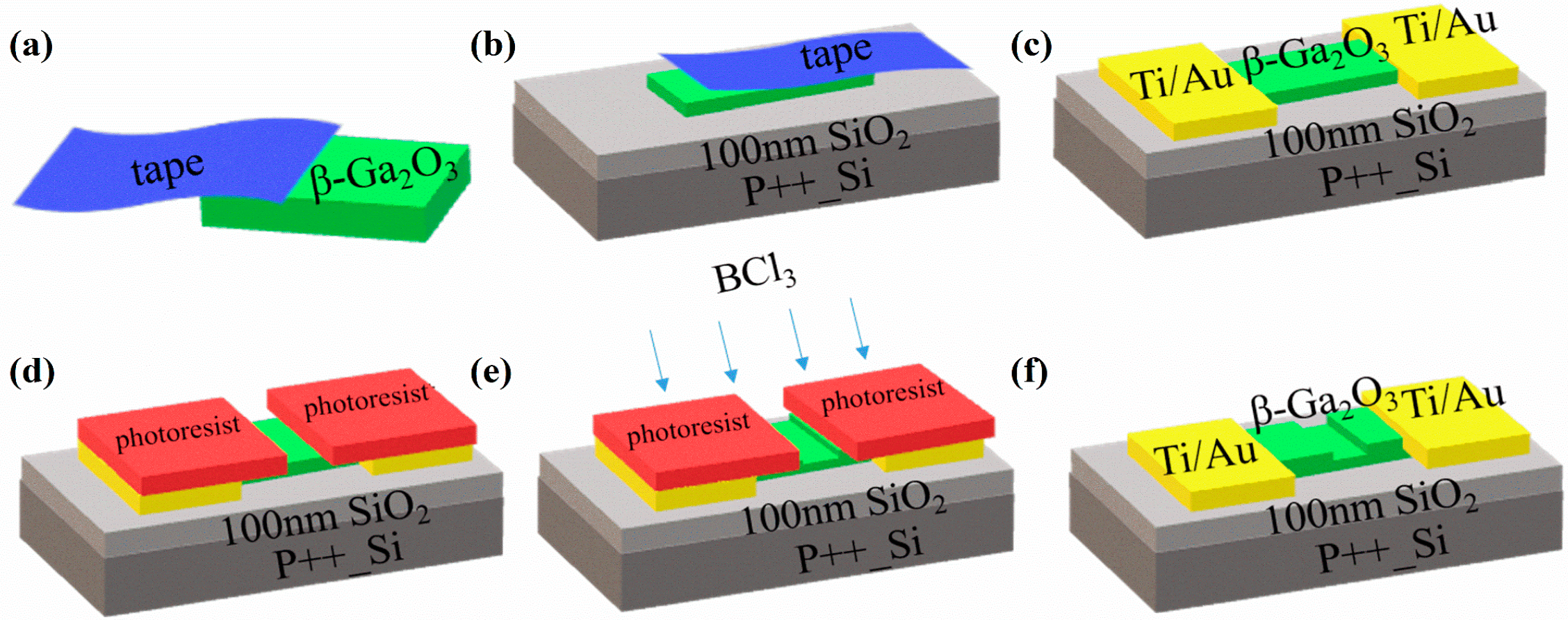
2. Materials and Methods
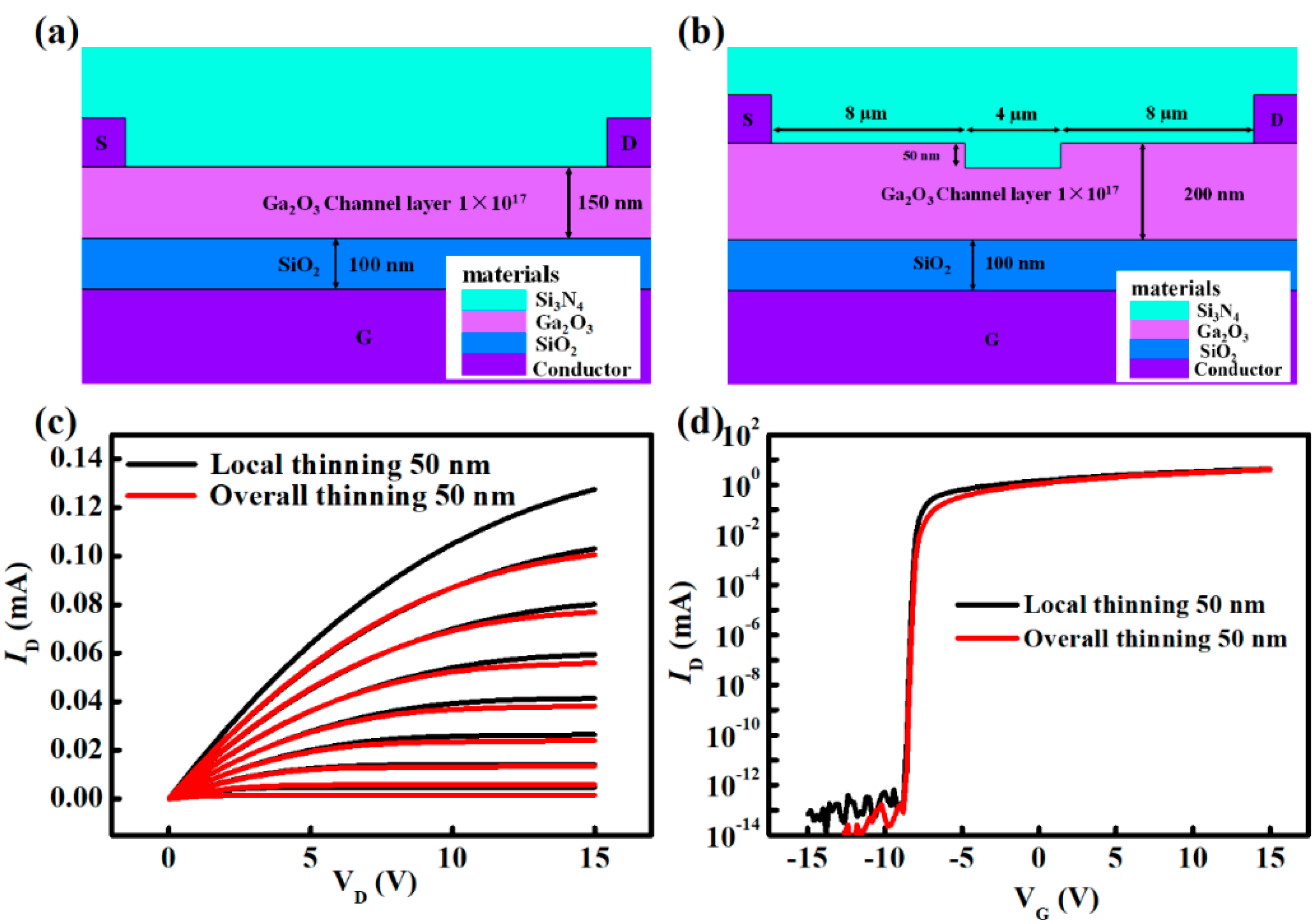
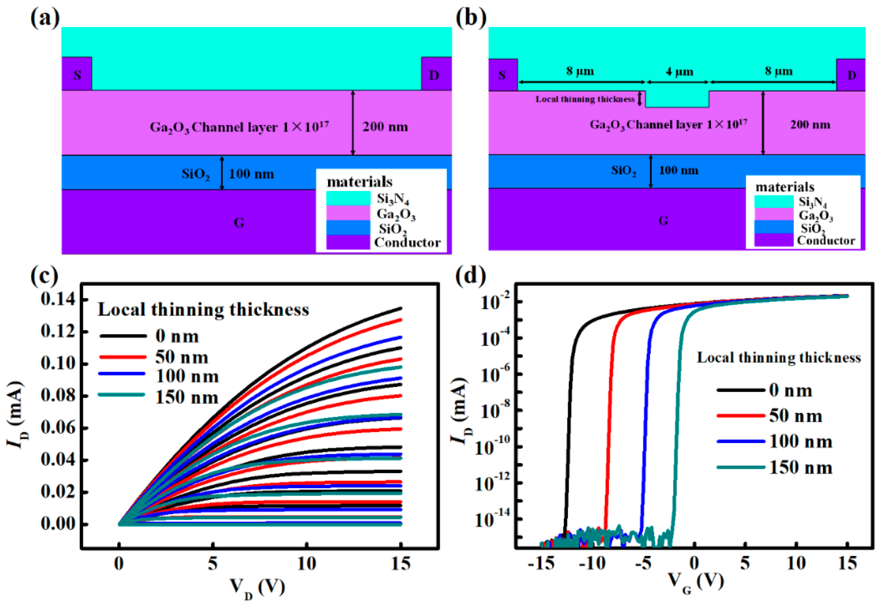
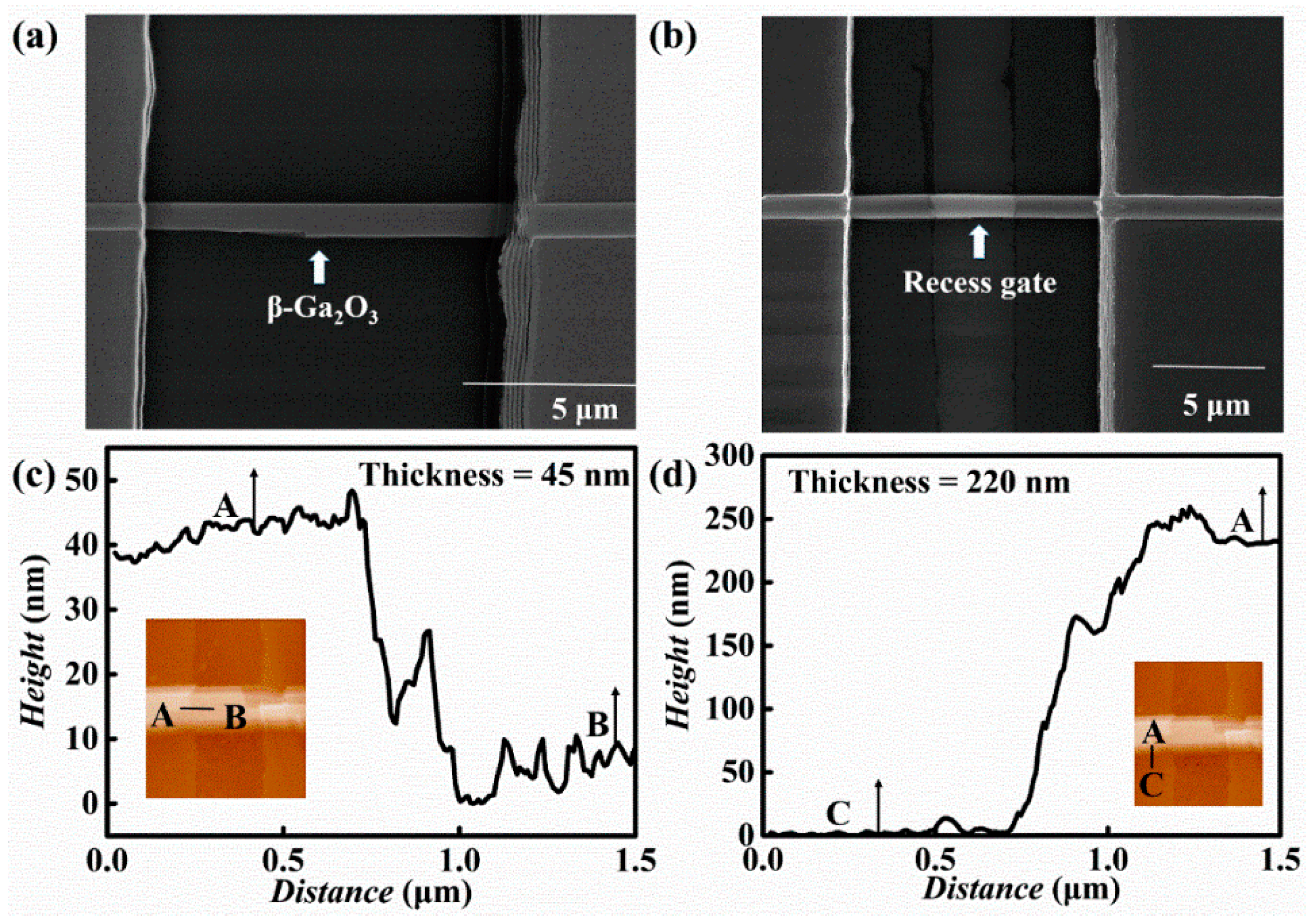
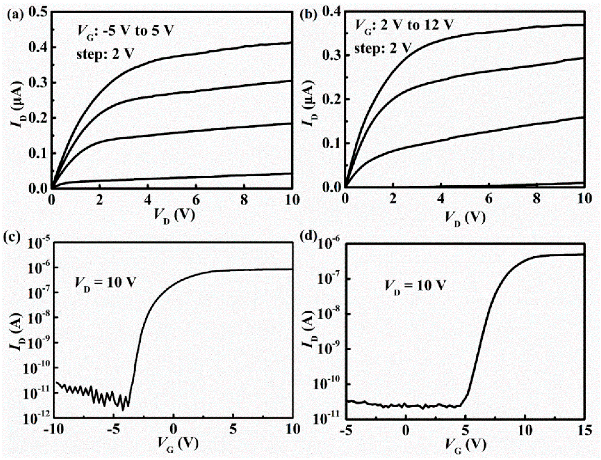
In this study, unintentionally doped bulk β−Ga2O3 crystals were used. The carrier concentration of the crystal is approximately 1 × 1017 cm−3. The arrangement of atoms in the monoclinic system β−Ga2O3 allows a facile exfoliate into thin flakes in the (100) direction, which has a larger lattice constant than other directions [9,34]. The device process flow is shown in Figure 1. First, nano−scale thickness Ga2O3 flakes were prepared by repeated mechanical exfoliation from the bulk Ga2O3 crystals. Then, Ga2O3 flakes were transferred to a p−type silicon wafer, with a 100 nm thickness thermally grown SiO2. For the Ga2O3 flakes to have better contact with the Si substrate and reduced amount of contaminants, the substrate was pretreated by oxygen plasma (ProCleanerTM, Harrick Plasma, Ithaca, NY, USA) for 3 min prior to the transfer. The source and drain electrodes were defined by Ti/Au (20 nm/80 nm) using an electron−beam evaporation technique on both ends of the Ga2O3 flakes. The source and drain contacts improved by inductively coupled plasma etching before electrode deposition with the power, chamber pressure, gas flow, and etching time of 150 W, 20 mTorr, BCl3/Ar (15 sccm/5 sccm) and 2 min, respectively. Finally, dry etching was performed using a BCl3/Ar plasma with a photolithography mask used to form the recess. The power, chamber pressure, gas flow, and etching time was 350 W, 20 mTorr, BCl3/Ar (15 sccm/5 sccm) and 3.5 min, respectively [35]. After etching, a Ga2O3 local thinning structure device was formed as shown in Figure 1f. The channel length and width are 12 μm and 1.1 μm, respectively.
The fabricated devices were characterized by scanning electron microscopy (SEM, FEI Nano 450, Hillsboro, OR, USA), atomic force microscopy (AFM, Benyuan CSPM5500, Guangzhou, China), and their electrical characteristics were measured using a source/measurement unit semiconductor parameter analyzer (Keysight B2902A, Santa Rosa, CA, USA) at room temperature.

3. Results

TCAD provides an efficient way to understand the properties of the device. Up to now, many related works have been reported on the TCAD simulation of Ga2O3 transistors [36,37,38]. Due to the non−convergence of the bottom gate model, we used a similar structure for the top gate to analyze the effect of the local thinning on the threshold voltage. Here, the effect of gate recess on the Ga2O3 FET with a doping concentration of 1017 cm−3 was investigated by modeling prior to device fabrication. In the model, the channel layer had a 200 nm thick Ga2O3 film and a gate dielectric layer of 100 nm SiO2. Figure 2 shows the simulation schematics with overall thinning of 50 nm (a) and local thinning of 50 nm (b), respectively. As shown in Figure 2c, comparing the output characteristic curves of the overall thinning and the local thinning, the current of the overall thinning is significantly smaller than that of the local thinning, but the transfer curves show that the threshold voltage of the overall thinning and the local thinning hardly changes, as shown in Figure 2d. This result indicates that local thinning can effectively prevent the current reduction caused by thinning Ga2O3 film.
Figure 3a,b shows the simulated structure of Ga2O3 FET without and with local thinning, respectively. To directly compare the Vth shift by increasing the locally thinned thickness, we set the thinning thickness to increase from 0 to 150 nm. Figure 3c shows the variation of the output current of Ga2O3 FETs with different thinning thicknesses. Obviously, with the increase in the local thinning depth, the output current gradually decreases. In addition, the thickness of the local thinning increases by 50 nm, and the threshold voltage is shifted in the positive direction by about 4 V, as shown in Figure 3d.
Based on the simulation results, β−Ga2O3 thin−film FET devices were prepared. Figure 4a and b show the SEM images of the β−Ga2O3 flake fabricated into a FET structure with a Ti/Au electrode and a FET device with local thinning, respectively. Figure 4c shows the local thinning depth is 45 nm and the bulk β−Ga2O3 crystal peeled off into a sheet with a thickness of approximately 220 nm, as revealed by the atomic force microscopy image, as shown in Figure 4d.
The output characteristics of the β−Ga2O3 FET with and without the local thinning structure were measured using a semiconductor characterization system at room temperature. In the measurements, the drain−source voltage ranges from 0 V to 10 V. The fabricated Ga2O3 FETs exhibited good saturation and pinch−off characteristics. As shown in Figure 5a and b, a linear increase in ID at low VD, and saturation at high VD, represent effective gate modulation in an n−type channel. A maximum drain current (IDmax) of 0.4 μA was obtained at the VG of +5 V in the device before etching, while the IDmax was just 0.34 μA at the VG of +12 V after etching, mainly because the etched oxide channel forms the local thinning. The local thinning structure also results in a low drain current. The transfer characteristics of the Ga2O3 FETs before and after etching were also measured. During the measurement, the device drain bias was set to +10 V. As shown in Figure 5c, the device before etching has a threshold voltage of −3 V, and after etching, the threshold voltage reaches +7 V, as shown in Figure 5d. This change is from a depletion mode to an enhanced field−effect transistor, mainly because the formation of a 45 nm local thinning structure after etching decreases the thickness of the channel layer, resulting in an earlier depletion pinch−off of the device during operation. Overall, the result is that Vth shifts from negative values in D−mode to positive values in E−mode by reducing the thickness of Ga2O3 [39]. The forward threshold voltage forms a normally on FET device. Comparing the off−state drain current before and after etching, the leakage current after etching is approximately 6 × 10⁻¹¹, which is larger than that of 8 × 10⁻¹² before etching, showing that dry etching damages the n−type Ga2O3 layer to some extent. Before the etching, the on/off current ratio of the device reaches 1 × 10⁵, because of the relatively low off−state current. After the etching, the on/off current ratio reduced to 2.2 × 10⁴, because of the rising leakage current.

4. Conclusions

In summary, Ga2O3 FETs were fabricated with and without the local thinning based on high−quality quasi−two−dimensional single−crystalline β−Ga2O3 flakes exfoliated from a bulk single crystal. The effect of the local thinning structure was investigated by device simulations. The simulation results show that the local thinning can achieve larger output current compared to the overall thinning. In addition, the threshold voltage shifted in the positive direction by about 4 V for every 50 nm increase in the locally thinned thickness. The fabricated Ga2O3 FETs have good saturation and pinch−off characteristics. In the device with a doping concentration of 1017 cm−3, the device before etching has a threshold voltage of −3 V, and after etching, the threshold voltage reaches +7 V. By optimizing the device processing, the performance of Ga2O3 FET may be further improved.

Author Contributions

M.X. and Q.X. conceived and designed the experiments; L.G., Q.C. and S.W. performed the experimental work and analyzed the data under the supervision of A.S., X.T., Z.J. and W.M.; writing—original draft preparation, L.G. All authors have read and agreed to the published version of the manuscript.

Funding

This work was supported by the Major Science and Technology Innovation Project of Shandong Province (Nos. 2019JZZY010210 and 2022CXGC010103).

Institutional Review Board Statement

Not applicable.

Informed Consent Statement

Informed consent was obtained from all subjects involved in the study.

Data Availability Statement

Not applicable.

Conflicts of Interest

The authors declare no conflict of interest.

References

  1. Mastro, M.A.; Kuramata, A.; Calkins, J.; Kim, J.; Ren, F.; Pearton, S. Perspective—opportunities and future directions for Ga2O3. ECS J. Solid State Sci. Technol. 2017, 6, P356. [Google Scholar] [CrossRef]
  2. Pearton, S.J.; Yang, J.; Cary, P.H.; Ren, F.; Kim, J.; Tadjer, M.J.; Mastro, M.A. A review of Ga2O3 materials, processing, and devices. Appl. Phys. Rev. 2018, 5, 011301. [Google Scholar] [CrossRef] [Green Version]
  3. Chen, J.X.; Li, X.X.; Ma, H.P.; Huang, W.; Ji, Z.G.; Xia, C.; Lu, H.L.; Zhang, D.W. Investigation of the Mechanism for Ohmic Contact Formation in Ti/Al/Ni/Au Contacts to beta−Ga2O3 Nanobelt Field−Effect Transistors. ACS Appl. Mater. Interfaces 2019, 11, 32127–32134. [Google Scholar] [CrossRef]
  4. Lv, Y.; Zhou, X.; Long, S.; Song, X.; Wang, Y.; Liang, S.; He, Z.; Han, T.; Tan, X.; Feng, Z.; et al. Source−Field−Plated β−Ga2O3 MOSFET with Record Power Figure of Merit of 50.4 MW/cm2. IEEE Electron Device Lett. 2018, 40, 83–86. [Google Scholar] [CrossRef]
  5. Chen, J.X.; Li, X.X.; Huang, W.; Ji, Z.G.; Wu, S.Z.; Xiao, Z.Q.; Ou, X.; Zhang, D.W.; Lu, H.L. High−energy X−ray radiation effects on the exfoliated quasi−two−dimensional beta−Ga2O3 nanoflake field−effect transistors. Nanotechnology 2020, 31, 345206. [Google Scholar] [CrossRef]
  6. Kim, J.; Kim, J. Monolithically Integrated Enhancement−Mode and Depletion−Mode beta−Ga2O3 MESFETs with Graphene−Gate Architectures and Their Logic Applications. ACS Appl. Mater. Interfaces 2020, 12, 7310–7316. [Google Scholar] [CrossRef]
  7. Kuramata, A.; Koshi, K.; Watanabe, S.; Yamaoka, Y.; Masui, T.; Yamakoshi, S. High−quality β−Ga2O3 single crystals grown by edge−defined film−fed growth. Jpn. J. Appl. Phys. 2016, 55, 1202A2. [Google Scholar] [CrossRef]
  8. Rafique, S.; Han, L.; Tadjer, M.J.; Freitas, J.A.; Mahadik, N.A.; Zhao, H. Homoepitaxial growth of β−Ga2O3 thin films by low pressure chemical vapor deposition. Appl. Phys. Lett. 2016, 108, 182105. [Google Scholar] [CrossRef]
  9. Kim, J.; Oh, S.; Mastro, M.A.; Kim, J. Exfoliated beta−Ga2O3 nano−belt field−effect transistors for air−stable high power and high temperature electronics. Phys. Chem. Chem. Phys. 2016, 18, 15760–15764. [Google Scholar] [CrossRef]
  10. Lv, Y.; Liu, H.; Wang, Y.; Fu, X.; Ma, C.; Song, X.; Zhou, X.; Zhang, Y.; Dong, P.; Du, H.; et al. Oxygen annealing impact on β−Ga2O3 MOSFETs: Improved pinch−off characteristic and output power density. Appl. Phys. Lett. 2020, 117, 133503. [Google Scholar] [CrossRef]
  11. Feng, Z.; Tian, X.; Li, Z.; Hu, Z.; Zhang, Y.; Kang, X.; Ning, J.; Zhang, Y.; Zhang, C.; Feng, Q.; et al. Normally−Off−β−Ga2O3 Power MOSFET With Ferroelectric Charge Storage Gate Stack Structure. IEEE Electron Device Lett. 2020, 41, 333–336. [Google Scholar] [CrossRef]
  12. Higashiwaki, M.; Sasaki, K.; Kuramata, A.; Masui, T.; Yamakoshi, S. Gallium oxide (Ga2O3) metal−semiconductor field−effect transistors on single−crystal β−Ga2O3 (010) substrates. Appl. Phys. Lett. 2012, 100, 013504. [Google Scholar] [CrossRef]
  13. Lu, X.; Zhang, X.; Jiang, H.; Zou, X.; Lau, K.M.; Wang, G. Vertical β−Ga2O3 Schottky Barrier Diodes with Enhanced Breakdown Voltage and High Switching Performance. Phys. Status Solidi (A) 2019, 217, 1900497. [Google Scholar] [CrossRef]
  14. Sdoeung, S.; Sasaki, K.; Kawasaki, K.; Hirabayashi, J.; Kuramata, A.; Oishi, T.; Kasu, M. Origin of reverse leakage current path in edge−defined film−fed growth (001) β−Ga2O3 Schottky barrier diodes observed by high−sensitive emission microscopy. Appl. Phys. Lett. 2020, 117, 022106. [Google Scholar] [CrossRef]
  15. Du, L.; Xin, Q.; Xu, M.; Liu, Y.; Liang, G.; Mu, W.; Jia, Z.; Wang, X.; Xin, G.; Tao, X.−T.; et al. Achieving high performance Ga2O3 diodes by adjusting chemical composition of tin oxide Schottky electrode. Semicond. Sci. Technol. 2019, 34, 075001. [Google Scholar] [CrossRef]
  16. Du, L.; Xin, Q.; Xu, M.; Liu, Y.; Mu, W.; Yan, S.; Wang, X.; Xin, G.; Jia, Z.; Tao, X.−T.; et al. High−Performance Ga2O3 Diode Based on Tin Oxide Schottky Contact. IEEE Electron Device Lett. 2019, 40, 451–454. [Google Scholar] [CrossRef] [Green Version]
  17. Moser, N.A.; McCandless, J.P.; Crespo, A.; Leedy, K.D.; Green, A.J.; Heller, E.R.; Chabak, K.D.; Peixoto, N.; Jessen, G.H. High pulsed current density β−Ga2O3 MOSFETs verified by an analytical model corrected for interface charge. Appl. Phys. Lett. 2017, 110, 143505. [Google Scholar] [CrossRef] [Green Version]
  18. Zhou, H.; Maize, K.; Qiu, G.; Shakouri, A.; Ye, P.D. β−Ga2O3 on insulator field−effect transistors with drain currents exceeding 1.5 A/mm and their self−heating effect. Appl. Phys. Lett. 2017, 111, 092102. [Google Scholar] [CrossRef] [Green Version]
  19. Wong, M.H.; Sasaki, K.; Kuramata, A.; Yamakoshi, S.; Higashiwaki, M. Field−Plated Ga2O3 MOSFETs With a Breakdown Voltage of Over 750 V. IEEE Electron Device Lett. 2016, 37, 212–215. [Google Scholar] [CrossRef]
  20. Green, A.J.; Chabak, K.D.; Baldini, M.; Moser, N.; Gilbert, R.; Fitch, R.C.; Wagner, G.; Galazka, Z.; McCandless, J.; Crespo, A.; et al. β−Ga2O3 MOSFETs for Radio Frequency Operation. IEEE Electron Device Lett. 2017, 38, 790–793. [Google Scholar] [CrossRef]
  21. Ahmadi, E.; Koksaldi, O.S.; Zheng, X.; Mates, T.; Oshima, Y.; Mishra, U.K.; Speck, J.S. Demonstration of β−(AlxGa1−x)2O3/β−Ga2O3 modulation doped field−effect transistors with Ge as dopant grown via plasma−assisted molecular beam epitaxy. Appl. Phys. Express 2017, 10, 071101. [Google Scholar] [CrossRef]
  22. Ahn, S.; Ren, F.; Kim, J.; Oh, S.; Kim, J.; Mastro, M.A.; Pearton, S.J. Effect of front and back gates on β−Ga2O3 nano−belt field effect transistors. Appl. Phys. Lett. 2016, 109, 062102. [Google Scholar] [CrossRef]
  23. Mohamed, M.; Janowitz, C.; Unger, I.; Manzke, R.; Galazka, Z.; Uecker, R.; Fornari, R.; Weber, J.R.; Varley, J.B.; Van de Walle, C.G. The electronic structure of β−Ga2O3. Appl. Phys. Lett. 2010, 97, 211903. [Google Scholar] [CrossRef]
  24. Leedy, K.D.; Chabak, K.D.; Vasilyev, V.; Look, D.C.; Boeckl, J.J.; Brown, J.L.; Tetlak, S.E.; Green, A.J.; Moser, N.A.; Crespo, A.; et al. Highly conductive homoepitaxial Si−doped Ga2O3 films on (010) β−Ga2O3 by pulsed laser deposition. Appl. Phys. Lett. 2017, 111, 012103. [Google Scholar] [CrossRef]
  25. Baldini, M.; Albrecht, M.; Fiedler, A.; Irmscher, K.; Klimm, D.; Schewski, R.; Wagner, G. Semiconducting Sn−doped β−Ga2O3 homoepitaxial layers grown by metal organic vapour−phase epitaxy. J. Mater. Sci. 2015, 51, 3650–3656. [Google Scholar] [CrossRef]
  26. Ahmadi, E.; Koksaldi, O.S.; Kaun, S.W.; Oshima, Y.; Short, D.B.; Mishra, U.K.; Speck, J.S. Ge doping of β−Ga2O3 films grown by plasma−assisted molecular beam epitaxy. Appl. Phys. Express 2017, 10, 041102. [Google Scholar] [CrossRef]
  27. Lv, Y.; Mo, J.; Song, X.; He, Z.; Wang, Y.; Tan, X.; Zhou, X.; Gu, G.; Guo, H.; Feng, Z. Influence of gate recess on the electronic characteristics of β−Ga2O3 MOSFETs. Superlattices Microstruct. 2018, 117, 132–136. [Google Scholar] [CrossRef]
  28. Chabak, K.D.; Moser, N.; Green, A.J.; Walker, D.E.; Tetlak, S.E.; Heller, E.; Crespo, A.; Fitch, R.; McCandless, J.P.; Leedy, K.; et al. Enhancement−mode Ga2O3 wrap−gate fin field−effect transistors on native (100) β−Ga2O3 substrate with high breakdown voltage. Appl. Phys. Lett. 2016, 109, 213501. [Google Scholar] [CrossRef] [Green Version]
  29. Hu, Z.; Nomoto, K.; Li, W.; Zhang, Z.; Tanen, N.; Thieu, Q.T.; Sasaki, K.; Kuramata, A.; Nakamura, T.; Jena, D.; et al. Breakdown mechanism in 1 kA/cm2 and 960 V E−mode β−Ga2O3 vertical transistors. Appl. Phys. Lett. 2018, 113, 122103. [Google Scholar] [CrossRef]
  30. Kamimura, T.; Nakata, Y.; Wong, M.H.; Higashiwaki, M. Normally−Off Ga2O3 MOSFETs With Unintentionally Nitrogen−Doped Channel Layer Grown by Plasma−Assisted Molecular Beam Epitaxy. IEEE Electron Device Lett. 2019, 40, 1064–1067. [Google Scholar] [CrossRef]
  31. Feng, Z.; Cai, Y.; Li, Z.; Hu, Z.; Zhang, Y.; Lu, X.; Kang, X.; Ning, J.; Zhang, C.; Feng, Q.; et al. Design and fabrication of field−plated normally off β−Ga2O3 MOSFET with laminated−ferroelectric charge storage gate for high power application. Appl. Phys. Lett. 2020, 116, 243503. [Google Scholar] [CrossRef]
  32. Wang, X.; Yan, S.; Mu, W.; Jia, Z.; Zhang, J.; Xin, Q.; Tao, X.; Song, A. Enhancement−Mode Ga2O3 FET With High Mobility Using p−Type SnO Heterojunction. IEEE Electron Device Lett. 2022, 43, 44–47. [Google Scholar] [CrossRef]
  33. Mu, W.; Yin, Y.; Jia, Z.; Wang, L.; Sun, J.; Wang, M.; Tang, C.; Hu, Q.; Gao, Z.; Zhang, J.; et al. An extended application of β−Ga2O3 single crystals to the laser field: Cr4+: β−Ga2O3 utilized as a new promising saturable absorber. RSC Adv. 2017, 7, 21815–21819. [Google Scholar] [CrossRef] [Green Version]
  34. Luo, H.; Jiang, H.; Chen, Z.; Pei, Y.; Feng, Q.; Zhou, H.; Lu, X.; Lau, K.M.; Wang, G. Leakage Current Reduction in β−Ga2O3 Schottky Barrier Diodes by CF4 Plasma Treatment. IEEE Electron Device Lett. 2020, 41, 1312–1315. [Google Scholar] [CrossRef]
  35. Liu, Y.; Du, L.; Liang, G.; Mu, W.; Jia, Z.; Xu, M.; Xin, Q.; Tao, X.; Song, A. Ga2O3 Field−Effect−Transistor−Based Solar−Blind Photodetector With Fast Response and High Photo−to−Dark Current Ratio. IEEE Electron Device Lett. 2018, 39, 1696–1699. [Google Scholar] [CrossRef] [Green Version]
  36. Kotecha, R.; Metzger, W.; Mather, B.; Narumanchi, S.; Zakutayev, A. Modeling and analysis of gallium oxide vertical transistors. ECS J. Solid State Sci. Technol. 2019, 8, Q3202. [Google Scholar] [CrossRef]
  37. Park, J.; Hong, S. −M. Simulation study of enhancement mode multi−gate vertical gallium oxide MOSFETs. ECS J. Solid State Sci. Technol. 2019, 8, Q3116. [Google Scholar] [CrossRef]
  38. Wong, H.Y.; Tenkeu, A.C.F. Advanced TCAD simulation and calibration of gallium oxide vertical transistor. ECS J. Solid State Sci. Technol. 2020, 9, 035003. [Google Scholar] [CrossRef]
  39. Zhou, H.; Si, M.; Alghamdi, S.; Qiu, G.; Yang, L.; Peide, D.Y. High−Performance Depletion/Enhancement−ode β−Ga2O3 on Insulator (GOOI) Field−Effect Transistors With Record Drain Currents of 600/450 mA/mm. IEEE Electron Device Lett. 2016, 38, 103–106. [Google Scholar] [CrossRef] [Green Version]
Figure 1. Schematic of the exfoliated β−Ga2O3−flake−based enhancement−mode FET fabrication process: (a) Nano−scale thickness β−Ga2O3 flakes were prepared by repeated mechanical exfoliation from the bulk Ga2O3 crystals, (b) β−Ga2O3 flakes were transferred to a p−type silicon wafer, (c) the schematic structure of the fabricated β−Ga2O3 flake FET, (d) the etched position of the local thinning after the FET device was subjected to a photolithography process, (e) etching to form the local thinning and (f) the schematic structure of the β−Ga2O3 flake FET with the local thinning.
Crystals 12 00897 g001
Figure 2. Schematic diagram of the simulation of the overall thinning of 50 nm (a) and the local thinning of 50 nm (b), output characteristic curves (c) and transfer characteristic curves (d) of overall thinning 50 nm and local thinning 50 nm.
Crystals 12 00897 g002
Figure 3. Schematic diagram of the simulation structure of bottom−gate Ga2O3 FET without (a) and with (b) local thinning, output characteristic curves (c) and transfer characteristic curves (d) of diiferent local thinning thickness.
Crystals 12 00897 g003
Figure 4. (a) SEM image of a β−Ga2O3 thin film made of a FET structure using a Ti/Au electrode, (b) SEM image of the local thinning of a Ga2O3 FET, (c) AFM height distribution of the local thinning and the Ga2O3 (d).
Crystals 12 00897 g004
Figure 5. (a) Output characteristic curve with various VG before and after (b) etching of β−Ga2O3 FET, the transfer curve in log scale before (c) and after (d) etching.
Crystals 12 00897 g005
Publisher’s Note: MDPI stays neutral with regard to jurisdictional claims in published maps and institutional affiliations.

