Article

Wafer−Scale Growth of Fe−Doped Hexagonal Boron Nitride (hBN) Films via Co−Sputtering

1
Key Laboratory for Physical Electronics and Devices of Ministry of Education and Shaanxi Provincial Key Laboratory of Photonics & Information Technology, Xi’an Jiaotong University, Xi’an 710049, China
2
School of Electronic Science and Engineering, Xi’an Jiaotong University, Xi’an 710049, China
3
Institute of Semiconductors, Chinese Academy of Sciences, Beijing 100083, China
4
National Centre for International Joint Research of Electronic Materials and Systems, School of Information Engineering, Zhengzhou University, Zhengzhou 450001, China
5
Institute of Materials and Systems for Sustainability, Nagoya University, Nagoya 464-8601, Japan
*
Author to whom correspondence should be addressed.
Crystals 2022, 12(6), 777; https://doi.org/10.3390/cryst12060777
Submission received: 24 April 2022 / Revised: 24 May 2022 / Accepted: 24 May 2022 / Published: 27 May 2022
(This article belongs to the Special Issue Wide-Bandgap Semiconductors)

Abstract

:
Fe−doped hBN film has great potential for use in spintronic applications. The wafer scale preparation of Fe−doped hBN films and their material properties are crucial for application in devices. In this work, Fe−doped films with 2−inch wafer scale were fabricated by magnetron co−sputtering, and the properties of the films were characterized. The crystal quality decreased, but the electrical performance was greatly improved. The average square resistance of Fe−doped film was 0.34 KΩ/sqr. Meanwhile, the Fe−doped films kept the characteristics of hBN well. The wavelength of absorption edge was 216 nm, and the corresponding optical band gap of 5.76 eV.

1. Introduction

Hexagonal boron nitride (hBN), a graphite−like layered compound, has gained a significant amount of attention due to its unique properties such as electrical insulation with a wide band gap of ~5.9 eV, high thermal conductivity, inherent flexibility, and high temperature stability [1,2,3]. The hBN film has been widely employed in deep ultraviolet (UV) light emitters [4,5], 2D−material based high−speed electronics [6,7], and resistance switching [8,9]. Furthermore, it has large potential applications for permanent magnetism and magnetic recording in the future [10]. However, the almost insulating property of the hBN material has limited its applications in electronic devices, which can be overcome by the doping method. Iron (Fe) atoms are easily reachable, and they can affect the optical, electronic, and magnetic properties of hBN. Based on density functional theory (DFT), the characteristics of Fe−doped hBN materials have been analyzed, especially the magnetism of thin films [11]. From the DFT calculation, the incorporation of iron could turn the semiconducting hBN sheet into a half−metal with a magnetic behavior, and the Fe−doped sheet could be useful for spintronic applications, such as tunneling magnetoresistance [12,13]. Few papers pay attention to the photoelectric properties of Fe−doped hBN films experimentally because it is difficult to prepare these films in a large area.
In this paper, Fe−doped hBN films with 2−inch wafer scale were fabricated by magnetron co−sputtering, and the material properties of the films were characterized. The morphology of the Fe−doped hBN film was observed by scanning electron microscope (SEM) and atomic force microscopy (AFM). Its properties were characterized by X−ray photoelectron spectroscopy (XPS), X−ray diffraction (XRD), Raman spectra, absorption spectra, and cathodoluminescence (CL).

2. Experiment Procedure

Fe−doped hBN film was prepared by the radio frequency (RF) magnetron co−sputtering method, using pure Fe and hBN of 99.99% as the co−target. The Ar ion bombards the target surface to provide the B, N, and Fe atoms for the film growth. In the process of preparation, a clean sapphire substrate was firstly put into the sputtering chamber and the substrate was heated when the chamber vacuum was pumped to 5 × 10⁻⁴ Pa. When the substrate temperature reached 600 °C, this temperature was maintained for 40 min. Next, the argon gas with 45 sccm was injected into the chamber and the chamber pressure was changed to 5 Pa. Meanwhile, the power supply of the co−target was set to be 175 W. In order to remove impurities and the oxide layer on the surface of the co−target, the pre−sputtering process was performed for 15 min when the baffle was closed. Then, the N2 of 15 sccm was injected into the chamber to replenish N vacancy in film formation and the chamber pressure was adjusted to 0.6 Pa. The baffle was opened and the Fe−doped hBN film began to be prepared. At last, target power and the central heater were turned off and the sample was taken out when the temperature of the chamber cooled to room temperature.

3. Results and Discussion

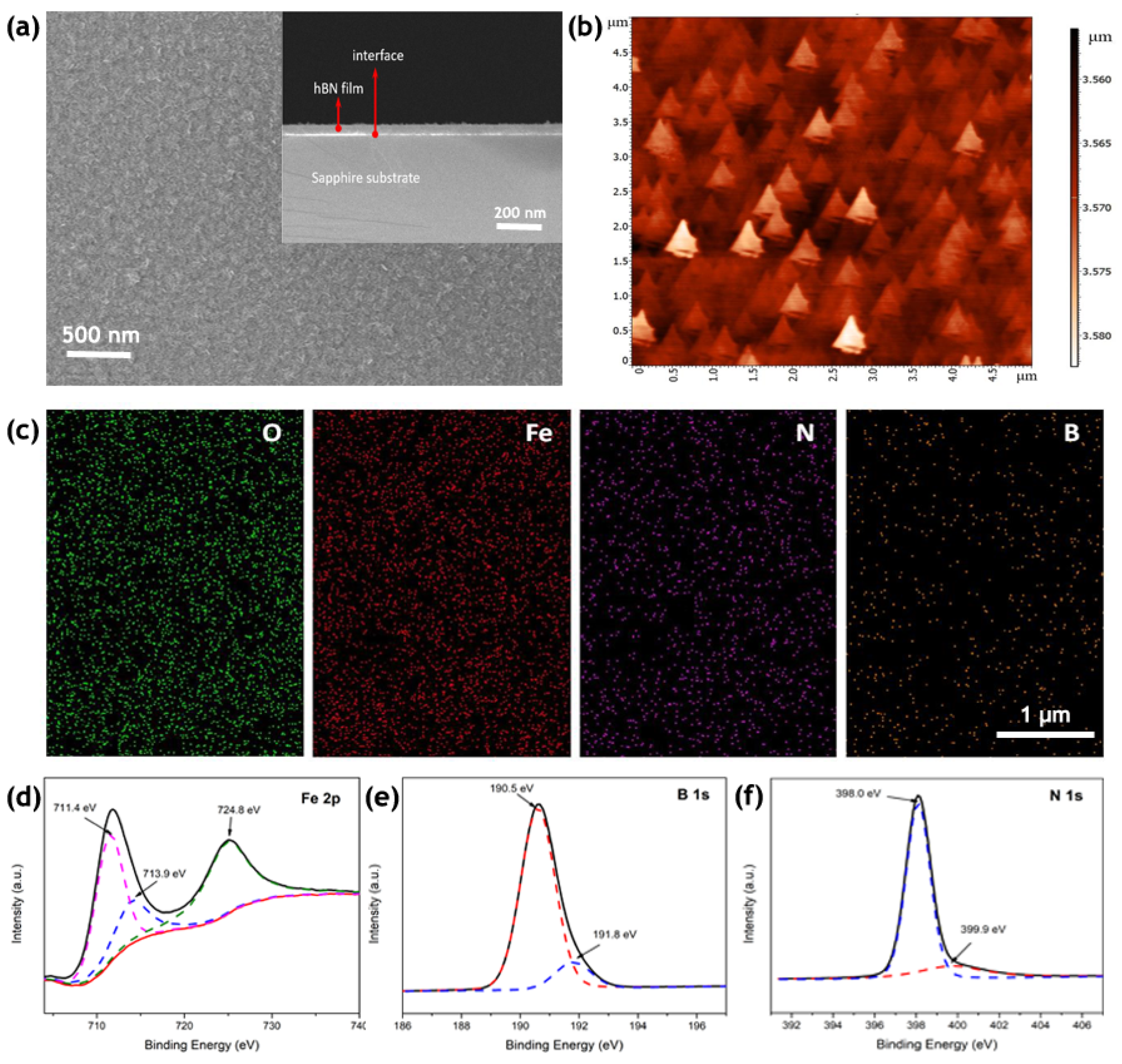
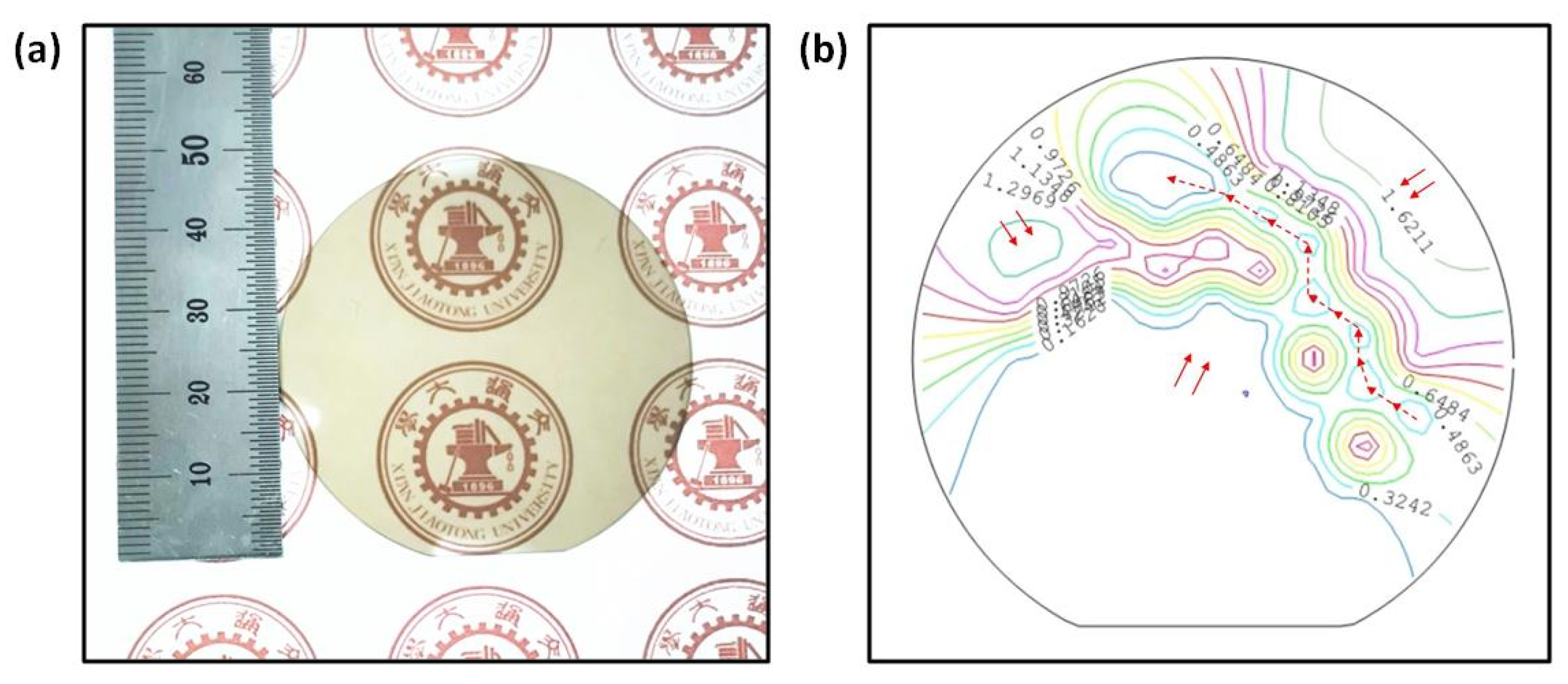
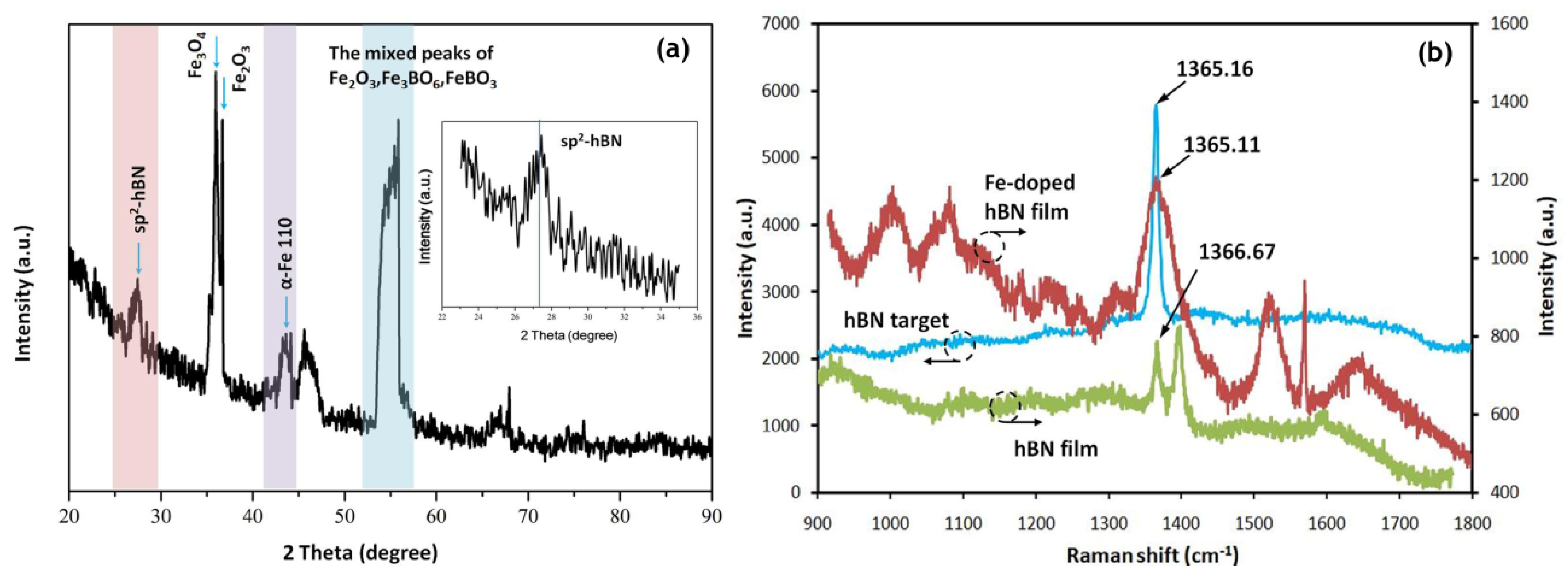
3.1. Morphology and Composition Analysis

Figure 1a shows the typical SEM images of the Fe−doped hBN film on a sapphire substrate prepared by magnetron sputtering technology. With 60 min deposition, a film with a thickness of 96 nm was obtained. A continuous and complete film was formed, the surface of which was relatively flat. Figure 1b shows the AFM image obtained by scanning an area of 5 μm × 5 μm with a root−mean−square (RMS) surface roughness of ~2.9 nm. At the beginning of film growth, the mono−oriented hBN triangular flakes (nanometer or micro size) were generally presented [14,15], and then they overlapped each other to form a large−scale continuous film [16]. As shown in Figure 1b, the whole surfaces showed unique triangle flakes, and these flakes were spliced together. This illustrated that the prepared Fe−doped hBN film could achieve good smoothness in a large area. Figure 1c shows the content distribution of each element (O, Fe, N, B) in the film from the energy dispersive spectrometer (EDS) results. The contents of O and Fe were much higher than those of N and B, indicating that the element of Fe exists in the form of oxide or simple substance. In parallel, the ratio of B and N showed the content of N element was higher than that of B element, which suggests that some Fe atoms replaced B atoms and bound to N atoms. Another reason for the weak signal of B element is that the signal of DES is inherently weak when characterizing light elements.
The XPS spectra of the fabricated Fe−doped hBN film are presented in Figure 1d–f. The XPS core level spectra can provide valuable information on the bonding mechanism in the film. In order to find out how boron atoms bond with nitrogen atoms inside the film in the case of Fe doping, the Fe 2p, B 1s and N 1s peaks from the XPS survey were deconvoluted. In the spectra of Fe 2p, the peaks of 711.4 eV and 724.8 eV represent the Fe–O bonds, corresponding to Fe2O3 and FeO respectively. The peak of 713.9 eV corresponds to the Fe–N bond. The core level spectrum of B 1s includes two peaks at 190.5 eV and 191.8 eV, which correspond to B–N bond and B–O bond, respectively. The peak of the B–O bond demonstrates that the films include a small amount of B2O3 or H3BO3 from the target [17,18,19]. For the spectrum of N 1s, the peak of 398.0 eV corresponds to N–B bonds. Additionally, there was a weak peak at 399.9 eV which was caused by the N–Fe bond. From the XPS spectra of Fe−doped hBN film, the main binding energies of the B 1s and N 1s orbital were at 190.78 eV and 398.30 eV, which mainly present the characteristics of hBN [16].

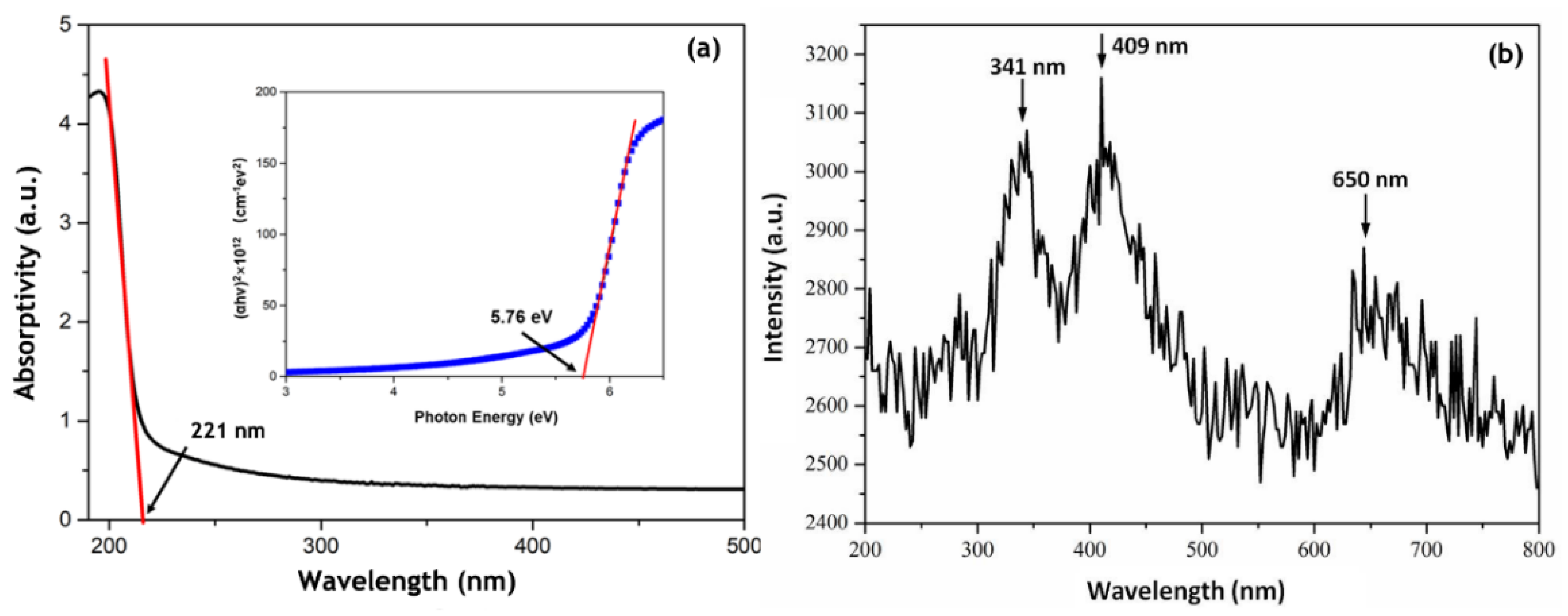
3.2. Film Properties

Figure 2a is a prepared Fe−doped hBN film on 2−inch sapphire with the thickness of 150 nm. The square resistance mapping test of the whole film during the growth was carried out, and the formation process was analyzed based on the change trend of square resistance. Figure 2b is the square resistance mapping in the film growth process. At the clamping position of the fixed substrate, the value of square resistance fluctuated due to the uneven stress, which has a great impact on the film formation. The area with uniform square resistance started from the area with uniform stress (arrow direction, solid line). In the middle area, an island chain (arrow direction, dotted line) was formed, and the continuous film formed based on the extended growth of these islands. It is well known that undoped hBN film is almost insulated. After Fe doping, the square resistance changed to 0.34 KΩ/sqr, which is the average value of 2−inch continuous film with 50 points.
Figure 3a shows the XRD patterns of the prepared sample. The characteristic peak of sp2−hBN is obvious at position of 26.8°, indicating that the Fe−doped hBN film retained the crystal structure of hBN, which is consistent with the XPS results of Figure 1d. The element of Fe is mainly composed of Fe3O4 and Fe2O3, corresponding to the peaks of 35.1° and 36°, respectively. Meanwhile, there was a wide peak from 53° to 57°, which was due to the superposition of the Fe–O–B bonds. The α−Fe also exists in the film, corresponding to the position of 43° in the spectrum. These results show that Fe atoms combined with the residual oxygen in the chamber to form iron oxides. From the Raman spectra in Figure 3b, the characteristic peaks of the prepared Fe−doped hBN film, undoped hBN film, and hBN target were highly consistent, which were 1365.11 cm−1, 1366.67 cm−1, and 1365.16 cm−1, respectively. The full−width at half−maximum (FWHM) of undoped hBN film was 14.33 cm−1, while that of Fe−doped hBN film was 49.18 cm−1. The FWHM of Fe−doped film significantly widened, indicating that the crystal quality decreased. Comparing the spectra of Fe−doped and undoped films, there were many secondary peaks caused by the compounds of Fe. There was a sapphire substrate peak at 1397.98 cm−1 in the spectrum of undoped hBN film, but a wave packet formed and covered this peak due to the broadening of the hBN peak in the spectrum of Fe−doped film. Meanwhile, it is noteworthy that a peak was generated at 1553 cm−1, which is a typical peak of γ−Fe2O3.
Figure 4a shows the UV−Vis absorption spectrum of the Fe−doped hBN film fabricated on a transparent sapphire substrate. A strong peak was observed at 202 nm in the absorption spectrum and the corresponding wavelength of absorption edge was 221 nm. This result is very close to the band edge absorption peak of hBN material, indicating that the spectral absorption of Fe−doped hBN film keeps the characteristics of hBN. By using the Tauc relationship [20], the optical band gap was determined to be 5.76 eV, as shown in the inset of Figure 4a, which is very close to theoretical calculations (5.9 eV) and the previous experimental data (5.84 eV) of hBN film [21,22].
Cathodoluminescence (CL) was used to further investigate the optical properties of Fe−doped hBN film. Figure 4b shows the CL spectrum of Fe−doped hBN film. The main peaks were located at 341 nm, 409 nm, and 650 nm, corresponding the band gaps of 3.65 eV, 3.02 eV, and 1.91 eV, respectively. There are two reasons to be considered. The first one is that the film mainly emits light at the impurity level. The Fe−doped hBN film presented an indirect band gap film based on DFT [11], so the electrons excited to the conduction band jump to the deep level (impurity level) firstly, and then recombination luminescence occurred. The second one is that film prepared by magnetron sputtering inevitably has many defects, and so the luminescence was caused by defects emission.

4. Conclusions

In summary, the 2−inch wafer scale Fe−doped hBN films were fabricated by magnetron co−sputtering, and the material properties of the films were characterized. In the prepared films, the main binding energies of the B 1s and N 1s orbital were at 190.78 eV and 398.30 eV, which mainly present the characteristics of hBN. Some Fe atoms combined with the residual oxygen to form iron oxides, and the Raman characteristic peak was located at 1365.11 cm−1. However, the FWHM significantly widened, indicating that the crystal quality decreased. The electrical performance was greatly improved, and the average square resistance of Fe−doped hBN film was 0.34 KΩ/sqr. Meanwhile, the Fe−doped hBN film kept the characteristics of hBN well. The wavelength of absorption edge was 216 nm, with a corresponding optical band gap of 5.76 eV. From the analysis of CL spectrum, the luminescence was caused by deep level recombination and defects emission. Looking forward, the wafer scale preparation of Fe−doped hBN films and the study of their photoelectric properties will greatly promote their application in devices.

Author Contributions

Q.L.: investigation, data curation and writing—original draft. Q.Z.: formal analysis—original draft. R.C.: investigation—review and editing. H.Z.: investigation. M.W.: investigation and formal analysis. J.Z.: conceptualization and methodology. X.W. and Y.L.: methodology. F.Y.: supervision. All authors have read and agreed to the published version of the manuscript.

Funding

The authors wish to thank the National Natural Science Foundation of China (No.61890961, No.61774121) and the National Key R&D Program of China (No.2021YFB3602000).

Institutional Review Board Statement

Not applicable.

Informed Consent Statement

Not applicable.

Data Availability Statement

Not applicable.

Acknowledgments

The EDS and XPS works were done at International Center for Dielectric Research (ICDR), Xi’an Jiaotong University.

Conflicts of Interest

The authors declare no conflict of interest and declare that they have no known competing financial interests or personal relationships that could have appeared to influence the work reported in this paper.

References

  1. Li, J.; Fan, Z.Y.; Dahal, R.; Nakarmi, M.L.; Lin, J.Y.; Jiang, H.X. 200 nm deep ultraviolet photodetectors based on AlN. Appl. Phys. Lett. 2006, 89, 213510. [Google Scholar] [CrossRef] [Green Version]
  2. Kobayashi, Y.; Akasaka, T.; Makimoto, T. Hexagonal boron nitride grown by MOVPE. J. Cryst. Growth 2008, 310, 5048–5052. [Google Scholar] [CrossRef]
  3. Kubota, Y.; Watanabe, K.; Tsuda, O.; Taniguchi, T. Deep ultraviolet light−emitting hexagonal boron nitride synthesized at atmospheric pressure. Science 2007, 317, 932–934. [Google Scholar] [CrossRef] [Green Version]
  4. Watanabe, K.; Taniguchi, T.; Kanda, H. Direct−bandgap properties and evidence for ultraviolet lasing of hexagonal boron nitride single crystal. Nat. Mater. 2004, 3, 404–409. [Google Scholar] [CrossRef]
  5. Watanabe, K.; Taniguchi, T.; Niiyama, T.; Miya, K.; Taniguchi, M. Far−ultraviolet plane−emission handheld device based on hexagonal boron nitride. Nat. Photonics 2009, 3, 591–594. [Google Scholar] [CrossRef]
  6. Dean, C.R.; Young, A.F.; Meric, I.; Lee, C.; Wang, L.; Sorgenfrei, S.; Watanabe, K.; Taniguchi, T.; Kim, P.; Shepard, K.L.; et al. Boron nitride substrates for high−quality graphene electronics. Nat. Nanotechnol. 2010, 5, 722–726. [Google Scholar] [CrossRef]
  7. Gannett, W.; Regan, W.; Watanabe, K.; Taniguchi, T.; Crommie, M.F.; Zettl, A. Boron nitride substrates for high mobility chemical vapor deposited graphene. Appl. Phys. Lett. 2011, 98, 242105. [Google Scholar] [CrossRef]
  8. Pan, C.; Ji, Y.; Xiao, N.; Hui, F.; Tang, K.; Guo, Y.; Xie, X.; Puglisi, F.M.; Larcher, L.; Miranda, E.; et al. Coexistence of grain−boundaries−assisted bipolar and threshold resistive switching in multilayer hexagonal boron nitride. Adv. Funct. Mater. 2017, 27, 1604811. [Google Scholar] [CrossRef]
  9. Li, Q.; Qin, X.; Zhang, Q.; Bai, Y.; Tang, H.; Hu, C.; Shen, S.; Li, Y.; Yun, F. Resistance switching behaviors of continuous−thick hBN films fabricated by radio−frequency−sputtering. J. Mater. Res. 2020, 35, 3247–3256. [Google Scholar] [CrossRef]
  10. Tizroespeli, F.; Parhizgar, S.S.; Beheshtian, J.; Boochani, A. Electronic, magnetic and optical properties of Fe−doped nano−BN sheet: DFT study. Indian J. Phys. 2020, 95, 823–831. [Google Scholar]
  11. Wang, M.; Meng, F.; Hou, D.; Han, Y.; Ren, J.; Bai, C.; Wang, B.; Zhou, T. Electronic structure and spin properties study on 2D h−BN nanosheet with Ti or Fe doping. Solid State Commun. 2020, 307, 113803. [Google Scholar] [CrossRef]
  12. Zhou, Y.G.; Xiao−Dong, J.; Wang, Z.G.; Xiao, H.Y.; Gao, F.; Zu, X.T. Electronic and magnetic properties of metal−doped BN sheet: A first−principles study. Phys. Chem. Chem. Phys. 2010, 12, 7588–7592. [Google Scholar] [CrossRef] [PubMed]
  13. Wu, R.Q.; Liu, L.; Peng, G.W.; Feng, Y.P. Magnetism in BN nanotubes induced by carbon doping. Appl. Phys. Lett. 2005, 86, 122510. [Google Scholar] [CrossRef] [Green Version]
  14. Wang, H.; Meng, F.; Zhu, B.; Leow, W.R.; Liu, Y.; Chen, X. Resistive Switching Memory Devices Based on Proteins. Adv. Mater. 2015, 27, 7670–7676. [Google Scholar] [CrossRef] [PubMed]
  15. Lee, K.H.; Shin, H.J.; Lee, J.; Lee, I.Y.; Kim, G.H.; Choi, J.Y.; Kim, S.W. Large−scale synthesis of high−quality hexagonal boron nitride nanosheets for large−area graphene electronics. Nano Lett. 2012, 12, 714–718. [Google Scholar] [CrossRef] [PubMed]
  16. Chen, T.A.; Chuu, C.P.; Tseng, C.C.; Wen, C.K.; Wong, H.P.; Pan, S.; Li, R.; Chao, T.A.; Chueh, W.C.; Zhang, Y.; et al. Wafer−scale single−crystal hexagonal boron nitride monolayers on Cu (111). Nature 2020, 579, 219–223. [Google Scholar] [CrossRef]
  17. Quan, H.; Wang, X.; Zhang, L.; Liu, N.; Feng, S.; Chen, Z.; Hou, L.; Wang, Q.; Liu, X.; Zhao, J.; et al. Stability to moisture of hexagonal boron nitride films deposited on silicon by RF magnetron sputtering. Thin Solid Films 2017, 642, 90–95. [Google Scholar] [CrossRef]
  18. Chen, L.; Zhou, M.; Luo, Z.; Wakeel, M.; Asiri, A.M.; Wang, X. Template−free synthesis of carbon−doped boron nitride nanosheets for enhanced photocatalytic hydrogen evolution. Appl. Catal. B Environ. 2019, 241, 246–255. [Google Scholar] [CrossRef]
  19. He, Z.; Kim, C.; Lin, L.; Jeon, T.H.; Lin, S.; Wang, X.; Choi, W. Formation of heterostructures via direct growth CN on h−BN porous nanosheets for metal−free photocatalysis. Nano Energy 2017, 42, 58–68. [Google Scholar] [CrossRef]
  20. Yuzuriha, T.H.; Hess, D.W. Structural and optical properties of plasmadeposited boron nitride films. Thin Solid Films 1986, 140, 199–207. [Google Scholar] [CrossRef]
  21. Ismach, A.; Chou, H.; Ferrer, D.A.; Wu, Y.; McDonnell, S.; Floresca, H.C.; Covacevich, A.; Pope, C.; Piner, R.; Kim, M.J.; et al. Toward the controlled synthesis of hexagonal boron nitride films. ACS Nano 2012, 6, 6378–6385. [Google Scholar] [CrossRef] [PubMed]
  22. Zhang, C.; Fu, L.; Zhao, S.; Zhou, Y.; Peng, H.; Liu, Z. Controllable co−segregation synthesis of wafer−scale hexagonal boron nitride thin films. Adv. Mater. 2014, 26, 1776–1781. [Google Scholar] [CrossRef] [PubMed]
Figure 1. (a) The top view and the cross−sectional SEM images of Fe−doped hBN film. (b) The AFM image of Fe−doped hBN film (5 μm × 5 μm). (c) The distribution of element content from EDS. (d) The XPS spectra of Fe 2p, (e) B 1s, and (f) N 1s.
Crystals 12 00777 g001
Figure 2. (a) Two inch wafer−scale film on sapphire with the thickness of 150 nm. (b) The square resistance mapping during the growth of thin film.
Crystals 12 00777 g002
Figure 3. The (a) XRD patterns and (b) Raman spectra of Fe−doped hBN film.
Crystals 12 00777 g003
Figure 4. (a) The UV−Vis absorption spectrum (b) the CL spectrum of Fe−doped hBN film. The insert shows optical band gap (5.76 eV) analysis of Fe−doped hBN from the absorption spectrum.
Crystals 12 00777 g004
Publisher’s Note: MDPI stays neutral with regard to jurisdictional claims in published maps and institutional affiliations.

