Article

Luminescence and Structural Characterization of Gd2O2S Scintillators Doped with Tb3+, Ce3+, Pr3+ and F for Imaging Applications

1
Dipartimento di Ingegneria Industriale e Scienze Matematiche, Università Politecnica delle Marche, 60131 Ancona, Italy
2
Dipartimento SIMAU, Università Politecnica delle Marche, 60131 Ancona, Italy
3
ICRYS Centro di Ricerca e Servizi di Analisi Globale dei Cristalli, Università Politecnica delle Marche, 60131 Ancona, Italy
4
Radiation Physics, Materials Technology and Biomedical Imaging Laboratory, Department of Biomedical Engineering, University of West Attica, 60131 Athens, Greece
5
Department of Biomedical Engineering, University of West Attica, 12210 Athens, Greece
6
Department of Biomedical Sciences, University of West Attica, 12210 Athens, Greece
*
Author to whom correspondence should be addressed.
Crystals 2022, 12(6), 854; https://doi.org/10.3390/cryst12060854
Submission received: 19 May 2022 / Revised: 10 June 2022 / Accepted: 14 June 2022 / Published: 17 June 2022
(This article belongs to the Section Inorganic Crystalline Materials)

Abstract

:
Radiodiagnostic technologies are powerful tools for preventing diseases and monitoring the condition of patients. Medicine and sectors such as industry and research all use this inspection methodology. This field demands innovative and more sophisticated systems and materials for improving resolution and sensitivity, leading to a faster, reliable, and safe diagnosis. In this study, a large characterization of gadolinium oxysulfide (Gd2O2S) scintillator screens for imaging applications has been carried out. Seven scintillator samples were doped with praseodymium (Pr3+), terbium (Tb3+) activators and co-doped with praseodymium, cerium, and fluorine (Gd2O2S:Pr,Ce,F). The sample screens were prepared in the laboratory in the form of high packing density screens, following the methodology used in screen sample preparation in infrared spectroscopy and luminescence. Parameters such as quantum detection efficiency (QDE), energy absorption efficiency (EAE), and absolute luminescence efficiency (ALE) were evaluated. In parallel, a structural characterization was performed, via XRD and SEM analysis, for quality control purposes as well as for correlation with optical properties. Spatial resolution properties were experimentally evaluated via the Modulation Transfer Function. Results were compared with published data about Gd2O2S:Pr,Ce,F screens produced with a standard method of a sedimentation technique. In particular, the ALE rose with the X-ray tube voltage up to 100 kVp, while among the different dopants, Gd2O2S:Pr exhibited the highest ALE value. When comparing screens with different thicknesses, a linear trend for the ALE value was not observed; the highest ALE value was measured for the 0.57 mm thick Gd2O2S:Pr,Ce,F sample, while the best MTF values were found in the thinner Gd2O2S:Pr,Ce,F screen with 0.38 mm thickness.

1. Introduction

X-ray radiation detection is fundamental in a number of fields spanning from research activities to industry, from health and security to environment monitoring and aerospace applications [1,2]. For instance, planar radiographic systems, as well as CT scanners and dosimetry systems, are largely used in medicine for diagnostic imaging and radiotherapies, in industry for quality assessment, and in scientific research as powerful tools for materials and systems investigations [3,4]. Those complex devices are based on a detection chain generally composed of a scintillating substance, which converts X-ray radiation into visible photons coupled to a photosensor, which finally converts the visible light into electrical signal-carrying information about the detected radiation [5,6]. The features of the signal depend on the characteristics of the scintillator. Its luminescence properties, as well as structural and morphological conditions, determine the performance of the detection device [7]. Sensitivity and spatial resolution are key parameters for achieving a fast and reliable analysis of the radiation environment. In diagnostic imaging, enhancing those parameters leads to an accurate and quick response of the imaging systems, allowing a lower dose and a shorter exposure of patients combined with a better-detailed depiction [2,4,5,6]. Scintillating single crystals or structured crystals are largely used due to their high-quality characteristics and performance [5]. However, in recent years, a great effort has been made to develop scintillating ceramics, aiming to substitute single crystals in some applications [8]. Although single crystals offer extraordinary performance, their production is a complex, multistage process making them costly and reducing ductility in terms of possible feasible geometries. On the other hand, ceramics are easily formable via powder sintering, molding, additive techniques, and other high-density packing processes [1,8]. In some applications, they offer suitable characteristics comparable to single crystals, providing cost reduction and formability of complex geometries [9,10].
This recent class of materials has been developed for use as phosphor screens in X-ray imaging applications. Gadolinium oxysulfide (Gd2O2S) based scintillators are some of the most promising due to their X-ray absorption efficiency [1,2,3]. In fact, those materials present high light yield (LY), density (7.32 g/cm3), and atomic number [1,2]. Small quantities of impurities (activators) are added to the phosphor substance to enhance the efficiency, speed of response, and optical matching optimization. Terbium-activated scintillators present an improved X-ray to visible light conversion, suitable with certain photosensors due to their emission spectra. Praseodymium doped Gadolinium oxysulfide shows a short decay time in good combination with the absorption efficiency of the host substance; therefore, it is suitable for reducing the blurring effect and for real-time imaging. Among the ultra-fast ceramics (UFC), the Gd2O2S co-doped by Praseodymium, Cerium, and Florine is a promising substance due to the low afterglow and an acceptable decay time [1]. In this study, activated Gd2O2S powders, in the form of test screens of different thicknesses, were subjected to luminescence, optical, and structural characterization in order to analyze the scintillating behavior with respect to dopant type and total sample thickness in parallel with the structural quality control of the compounds. The evaluation of imaging properties was carried out to quantify the final image reproduction potentialities. Trivalent ions such as terbium (Tb3+), praseodymium (Pr3+), and cerium (Ce3+), in addition to fluorine (F), were used as single activators or properly combined in the same powder sample. In fact, the incorporation of F ions decreased thermoluminescence intensity, as described in [11]. This result suggests that F ions substituting for O2− or S2− ions of the host lattice can compensate for intrinsic defects resulting in increased efficiency. Furthermore, co-doping with Ce3+ or F was found to have significant impacts on the scintillation properties, such as light output and afterglow [11,12,13].
Absolute Luminescence Efficiency (ALE), Quantum Detection Efficiency (QDE), and Energy Absorption Efficiency (EAE) were measured and calculated for luminescence and X-ray absorption efficiency quantification [14,15]. Those parameters are crucial for dose and exposure management and reduction during acquisitions. An evaluation of the Modulation Transfer Function (MTF) was carried out for imaging properties characterization [16]. This characterization of the GOS function properties was conducted in parallel with a structural evaluation of the composites. X-ray diffraction (XRD), scanning electron microscopy (SEM), and energy-dispersive X-ray spectroscopy microanalysis (EDS) were used to investigate the samples’ microstructure quality [17,18]. Structural characteristics such as crystallinity, size, and morphology of the powder particles are at the base of the absorption and light performance of the substances; X-ray interaction, light production, reabsorption, and scattering are strongly determined by the matter’s micro and macro structure quality. Quality control is, therefore, mandatory for the production of proper samples.
The results of this characterization confirm the suitability of the samples for use in imaging applications. The measured data were analyzed and discussed as a function of the structural condition (microstructure characteristics) and the geometry, providing an idea of the optimal X-ray energy versus sample thickness combination, validated in a radiation regime similar to the medical environment.

2. Materials and Methods

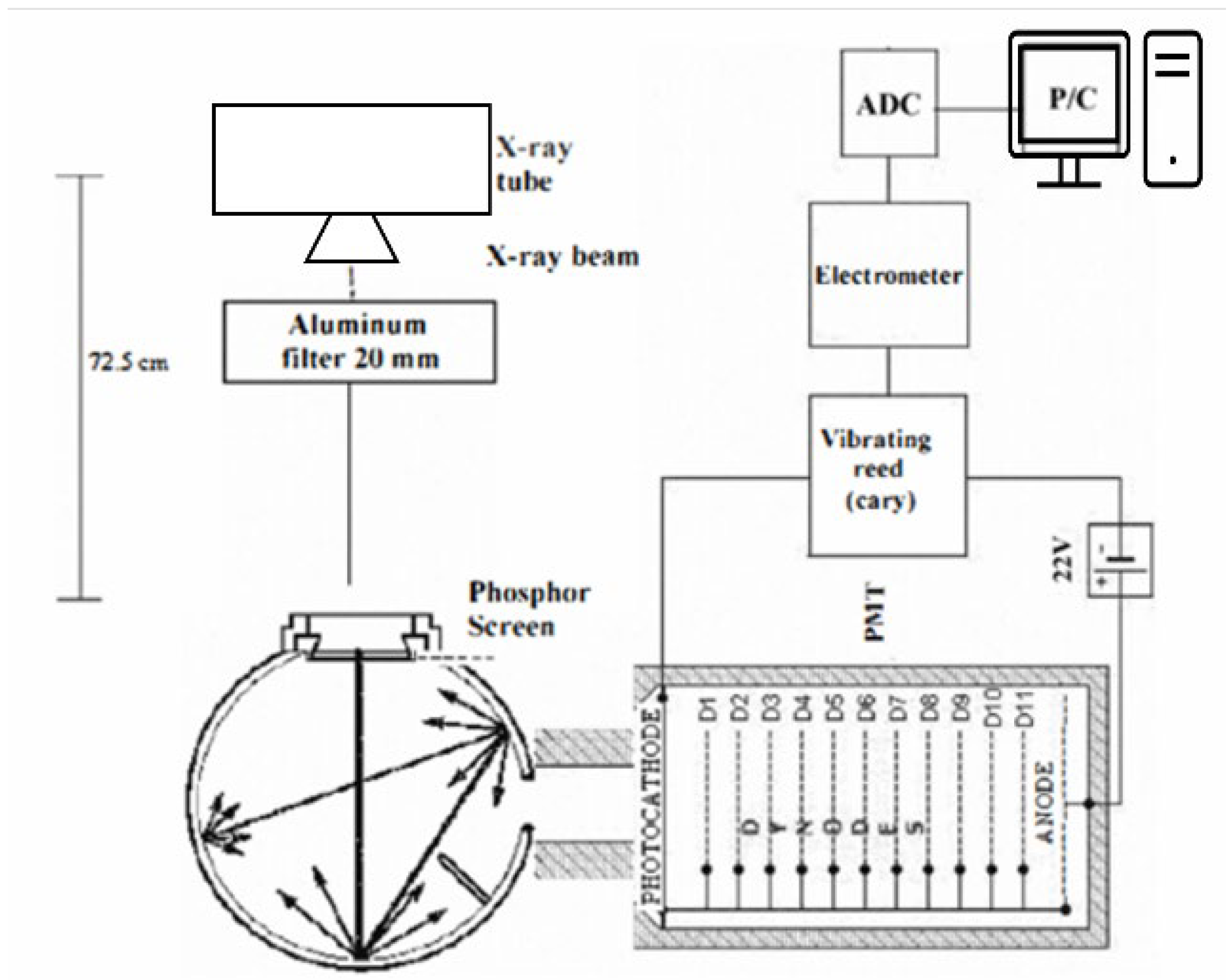
2.1. Sample Preparation and Irradiation Conditions

In the present study, seven powder scintillators based on Gd2O2S in the form of high packing density screens were prepared in a vacuum using a hydraulic press. Each screen was produced by mixing Gd2O2S and potassium bromide (KBr) powders in the same percentage (50%) in the form of a disk with a 1.3 cm2 surface area [15], following the methodology of pellet preparation in infrared spectroscopy [19]. Potassium bromide is commonly used as a binding material in applications such as infrared spectroscopy to obtain homogeneous powders that can be compacted into diaphanous KBr solid pellets [20]. The potassium bromide melts under pressure and seals the compound into a matrix. Phosphor and KBr powders were ground together with an agate pestle until the compounds were well dispersed. Each sample was put under vacuum for approximately 2 min in order to remove the air, and then pressed under 10 kN for one minute, using a hydraulic press. The result was translucent screens that were used for experimental evaluation. Gd2O2S was purchased in powder form with a mean grain size of approximately 16.0 µm (as stated by the vendor, Phosphor Technology Ltd., datasheet). The Gd2O2S scintillator material has an effective atomic number equal to Zeff = 61.1 with a density of 7.34 g/cm3 [8,21].
Table 1 lists the samples produced by the described technique. In single doped samples #S1 and #S2, with the same thickness (0.38 mm), Pr and Tb were used as activators, respectively (Table 1). The multi-doped samples (#M1–#M5) have the same composition, consisting of Gd2O2S mixed with the same combination of 3 different activators (Pr, Ce, and F), produced in different thickness values (0.38, 0.57, 0.68, 0.88, and 1.1 mm) in order to investigate the influence of thickness on the luminescence efficiency behavior (Table 1). Additionally, the amount of the dopants in each composition is nominally about 1%.
Each scintillator sample screen was exposed to X-rays on a BMI General Medical Merate tube with rotating tungsten anode and inherent filtration equivalent to 2 mm Al, with energies ranging from 50 to 130 kVp (typical range used in general radiography and fluoroscopy). The 3 energy fluence spectra for the selected X-ray tube voltages of 70, 100, and 130 kVp are presented in Figure 1. An additional filtration was introduced in the beam to simulate beam quality alteration by a human body by inserting a 20 mm aluminum plate [22,23].

2.2. Structural Characterization

Structural characterization was carried out by X-ray diffraction (XRD) and scanning electron microscopy (SEM). A Bruker D8 Advance diffractometer (provided by Bruker, Billerica, MA, USA) operating with Cu-Kα radiation in the angular range 2θ = 5°–80° at V = 40 kV and I = 40 mA was used for XRD investigation. Peak shape analysis was carried out with the Origin software package to obtain an exact angular position and width that allowed for estimating the samples’ lattice parameters. Phase analysis of XRD patterns was performed by the DIFFRAC.EVA (Version 7, provided by Bruker, Billerica, MA, USA) search/match software package (Bruker AXS) using the powder diffraction database (PDF) of the International Centre for Diffraction Data (ICDD).
Scanning electron microscopy observations were carried out with a field emission SEM (FESEM) ZEISS SUPRA 40 equipped with a Bruker Z200 microanalysis (EDS) (provided by ZEISS, Carl-Zeiss-Strasse 22, 73447 Oberkochen, Germany).

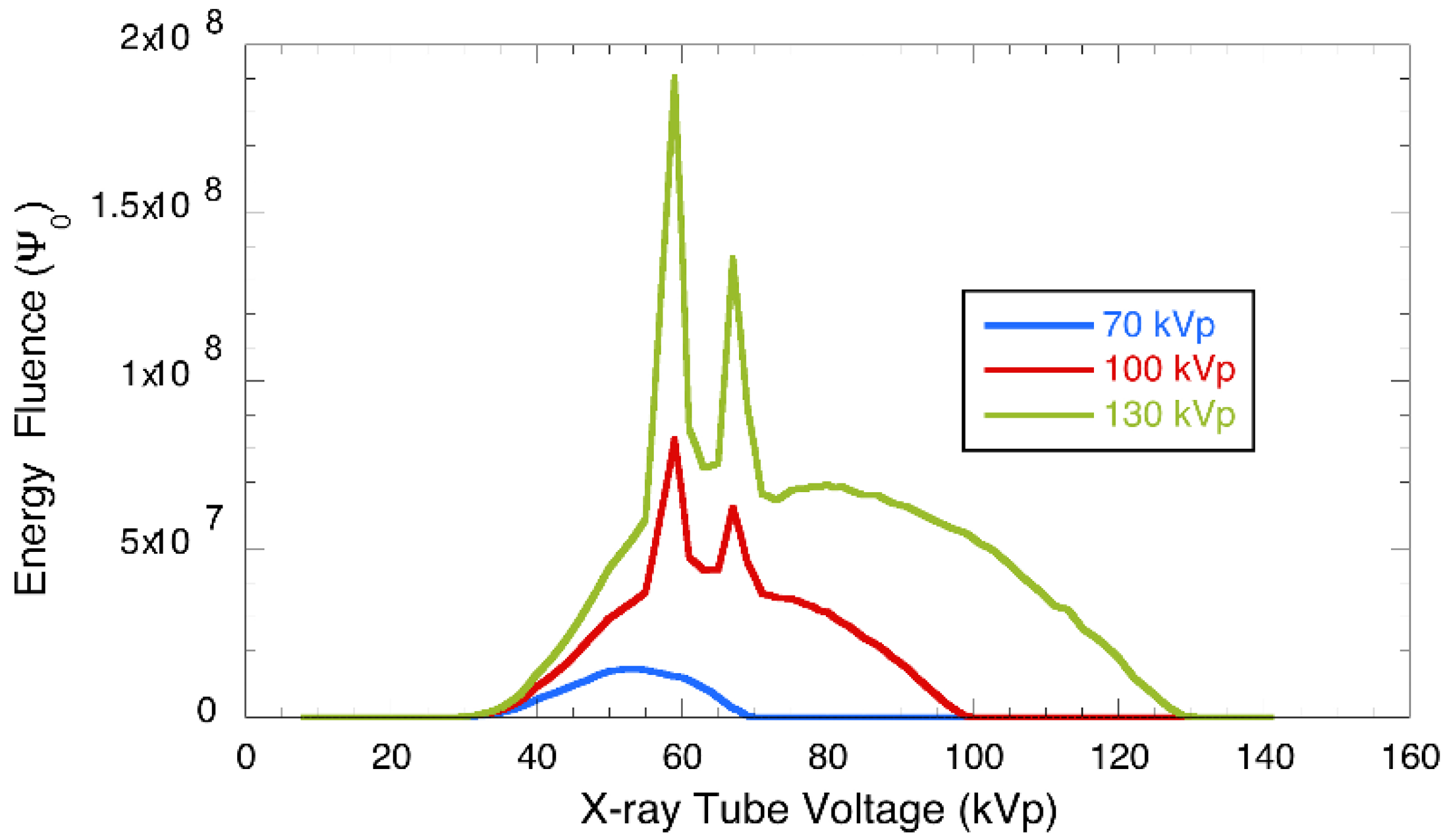
2.3. Radiation Detection Parameters and Emission Spectra

The efficiency of a phosphor screen in detecting X-ray photons is estimated with the quantum detection efficiency (QDE) [24,25,26]. This parameter is related to the attenuation coefficient and the thickness of the scintillating material. QDE is the fraction of incident photons interacting within the scintillator mass. For polyenergetic X-ray beams, QDE is averaged over the X-ray spectrum as follows:
QDE ( E ) = [ 0 E 0 Φ 0   ( E ) ( 1 e ( μ tot , t ( E ) ρ ) W ) dE ]   ( 0 E 0 Φ 0 ( E ) dE ) 1
where E indicates the X-ray photon energy, Ε 0 is the maximum energy of the X-ray spectrum, Φ 0   (E) is the X-ray spectrum (photon fluence) measured as X-rays/mm2 and μ tot , t ( E ) ρ is the X-ray total mass attenuation coefficient of the scintillator, computed using XMudat software [24]. W is the density of the phosphor screen related to its coating thickness (in units of mg/cm2). The denominator in (1) expresses the total X-ray photon flux incident on the detector.
Since X-ray imaging detectors are integrating systems, their output signal is proportional to the amount of X-ray energy absorbed within the scintillator. For this reason, when evaluating X-ray imaging systems, there is another important parameter to consider, the energy absorption efficiency (EAE) [27].
EAE describes the fraction of the incident energy locally absorbed at the point of X-ray interaction within the scintillator [14,28]. It is related to the amount of energy deposited in the phosphor mass, which, in turn, is directly related to the amount of light generated and detected by the optical sensor and contributes to image formation. EAE can be estimated for polyenergetic X-ray beams as follows:
EAE ( E ) = [ 0 E 0 Φ 0   ( E ) E ( μ tot , en ( E ) μ tot , t ( E ) ) ( 1 e ( μ tot , t   ( E ) ρ ) w ) dE ] ( 0 E 0 Φ 0   ( E ) dE ) 1  
where Φ 0 ( E ) E = Ψ 0 ( Ε ) is the incident X-ray energy fluence. μtot,en is the total mass energy absorption coefficient of the scintillator, in which all the mechanisms of local energy deposition at the first point of X-ray interaction within the mass of the scintillator are considered.
Both the QDE and EAE can be increased by making the scintillator/phosphor screen thicker or by using materials with higher values of atomic number and density. The radiation detection will usually be highest at low energies, and it decreases with increasing energy [28], however, showing an increase in the K-edge energy.
The emitted light spectra of the powder phosphor samples were measured using an Oriel grating optical spectrometer (Ocean Optics Inc., Dunedin, FL, USA, HR2000) under X-ray excitation conditions. The emitted light spectrum was transferred by an FCB-UV400-2 Avantes optical fiber (Avantes company, Avantes B.V., Oude Apeldoornseweg 28, 7333 NS Apeldoorn, The Netherlands).

2.4. Absolute Luminescence Efficiency (ALE)

The luminescence of the screens was evaluated by measuring the absolute luminescence efficiency (ALE). ALE is the parameter used to describe the radiation detection sensitivity of energy integrating detectors. Each phosphor sample was positioned inside an integration sphere (Oriel 70451, MKS Newport corporation, Deere Avenue Irvine, CA, USA), used to decrease errors related to the angular distribution of the emitted light beam. The light emitted by the irradiated phosphor was measured with a calibrated photomultiplier (EMI 9798B, ET Enterprises, Ltd., 45 Riverside Way, Uxbridge, UK) equipped with a photocathode (extended S20 EMI). The photocathode was directly connected to a Cary 401 (Cary instruments, distributed by Agilent, Headquarters, 5301 Stevens Creek Blvd., Santa Clara, CA, USA) vibrating reed electrometer. Each sample screen was exposed to X-rays generated by a radiographic unit. X-ray tube voltage ranged from 50 to 130 kVp. An additional plate (filter) with a 20 mm thickness of aluminum was added in order to simulate the passage of the beam through the patient’s body [22,23]. A scheme of a typical experimental setup [29] is illustrated in Figure 2.
ALE is calculated according to the following relation [22,23,30]:
ALE =   Ψ ˙ λ ( X ˙ ) 1 =   Ψ ˙ λ X ˙
where Ψ ˙ λ is the light energy flux emitted by a scintillator or a phosphor when irradiated by X-rays and X ˙ is the exposure rate incident on the phosphor. Conversions of the electrometer’s output current and dosimeter data can be found at [31]. The absolute luminescence efficiency is measured in efficiency units—E.U [1 E.U = 1 μW m−2/mR s−1] [22,23].
In radiology applications, having a scintillator material with high ALE reduces the amount of the radiation dose to the patient and the time of acquisition.

2.5. Parameters of Image Quality: Modulation Transfer Function (MTF)

The capability of reproducing object details in a 2D or 3D image is a fundamental parameter of an imaging system. This quality is crucial in diagnostic images, allowing reliable monitoring, inspection, and, consequently, effective decisions, all critical for medical applications. The reproduction capability of an imaging system can be described by the modulation transfer function (MTF) parameter, which combines contrast and resolution in one standard measure and is expressed in line pairs or cycles per millimeter (lp mm−1 or Cycles mm−1). The MTF defines contrast reduction as a function of spatial frequencies that compose a test target. MTF can be mathematically calculated as the ratio of the output modulation Mout to the input modulation Min to a sinusoidal signal at spatial frequency f. The modulation M is the ratio of the amplitude of the signal to the average of the signal. MTF has a maximum value at zero spatial frequency, and it then drops in a systemic-specific manner down to zero with increasing frequency defining how close two features can be to be properly distinguished by the imaging system. The limiting spatial resolution of the system is often considered as the spatial frequency at which the MTF crosses the 10% level. This means that the human observer is not able to detect details that have less than 10% contrast with respect to large area objects.
MTF can be calculated through different methods. In this study, the slanted-edge technique was chosen [16]. This technique is based on the calculation of the edge spread function (ESF), which describes the response of the detector to a radiopaque sharp-edge test object (usually tungsten metal). The purpose of the edge is to obtain an X-ray image with transmitted radiation on one part and almost perfect attenuation on the other. The width of ESF is calculated as the distance required rising from 10% to 90%. Once the ESF has been estimated, the Fast Fourier Transform (FFT) is applied to obtain the corresponding MTF curves.
All powder screens examined in this study were enclosed in a light-tight radiographic cassette (24 × 30) in contact with radiographic film (Kodak T-Mat). The screen–film combination was irradiated with a constant energy of 70 kVp and a current of 63 mA (according to the RQA-5 protocol, International Electrotechnical Commission (IEC 62220-1-1:2015) [32]. The modulation transfer function of sample screens was determined through the Slanted-Edge method technique. The MTF was measured using a PTW Freiburg tungsten edge test device, following the procedures described in the IEC standard and analytically explained in [16]. Films were developed in an Agfa Scopix LR 5200 film processor. Edge images obtained on the films were digitized in an Agfa Duoscan scanner. The MTF data obtained in this way were not corrected by dividing the MTF of the film and the MTF of the scanner, assuming that they have MTF = 1 in spatial frequencies (up to 30 cycles/cm) examined in this study.

3. Results and Discussion

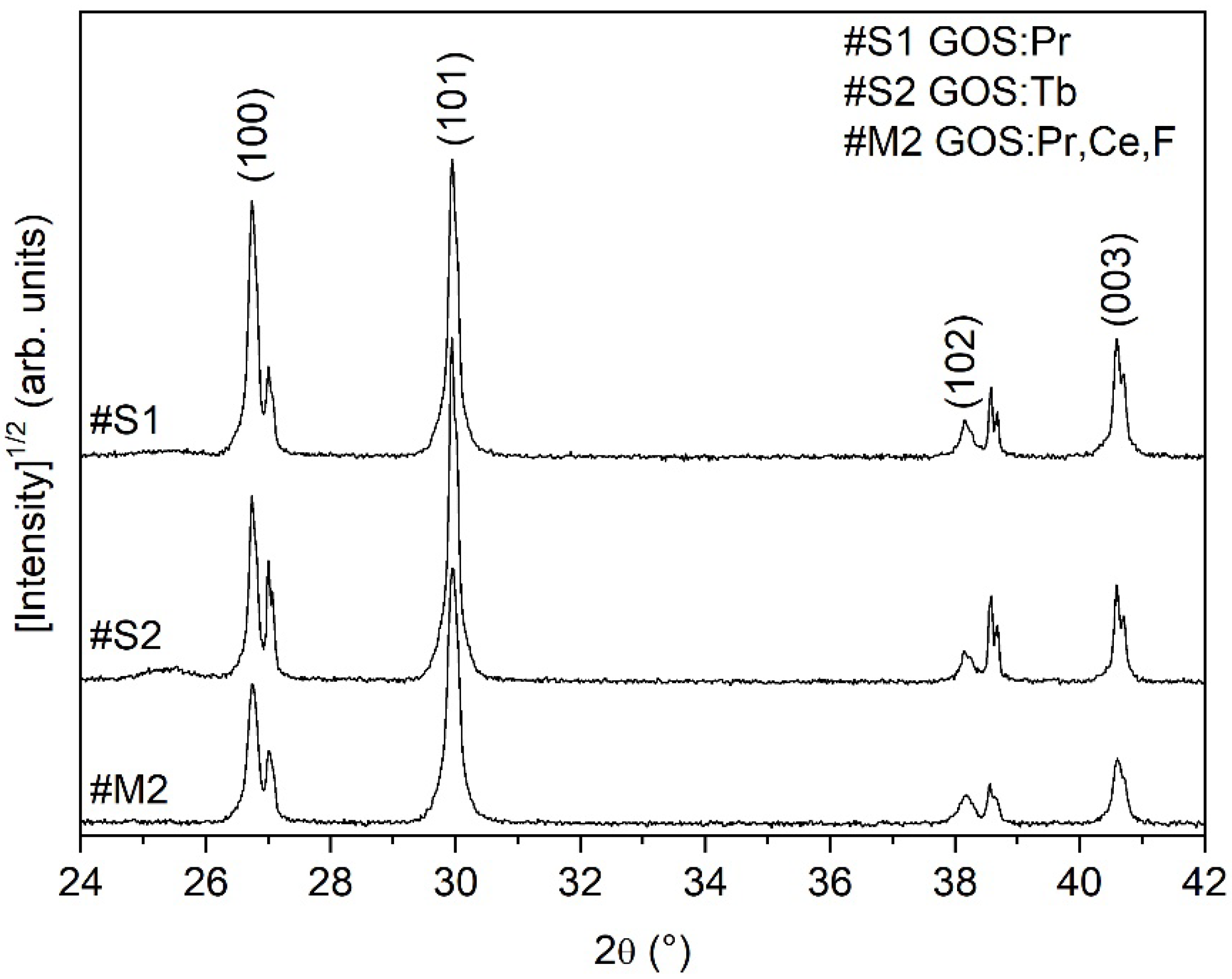
3.1. X-ray Diffraction (XRD)

XRD patterns of all samples, analyzed in the same condition, evidenced the simultaneous presence of Gd2O2S (ICDD file n. 26-1422) and KBr (ICDD file n. 36-1471). Gd2O2S (GOS) is a hexagonal (hcp) compound with nominal lattice parameters a = 0.3852 nm and c = 0.6667 nm, while KBr is cubic (fcc) with a = 0.66005 nm.
Figure 3 shows the XRD patterns of GOS:Pr (#S1), GOS:Tb (#S2), and GOS:Pr,Ce,F (#M2) in the angular range 2θ = 24°–42°, where the most intense peaks of the Gd2O2S compound are located. XRD patterns in Figure 3 are shown in square root scale ([Intensity]1/2) to enhance low-intensity peaks. Peak shape analysis and quantitative measurements were carried out on original patterns in the angular range 2θ = 5°–80°. In Figure 3, peaks of the Gd2O2S compound are indexed by the corresponding Miller indices, while the unindexed peaks are due to KBr, which was used for screen preparation.
Peak shape analysis of the XRD patterns allowed obtaining the exact angular position of peaks, from which the experimental lattice parameters of the Gd2O2S compound in each sample were estimated. Experimental values of lattice parameters for Gd2O2S are listed in Table 2, with the reference values from the ICDD database (file n. 26-1422) reported for comparison.
Within experimental uncertainties, measured samples have equal lattice parameter values. The experimental crystallographic cell volume calculated from lattice parameters values in Table 2 is Ve = 0.0855 ± 0.0001 nm3 for all samples, which must be compared to the reference cell volume Vr = 0.08567 nm3. Therefore, from the crystallographic point of view, the experimental values in Table 2 show that the material used for screen production is the hexagonal Gd2O2S compound, which results in being substantially unmodified by the addition of different activators.
Peak shape analysis also allowed calculating the relative intensity of Gd2O2S peaks visible in Figure 3, and results are reported in Table 3, with the reference values from the ICDD database (file n. 26-1422) reported for comparison.
Deviations of the experimental values from the reference are clearly evident in Table 3, suggesting the different influence of the activator type on the hosting material’s microstructure. In particular, single (#S1 and #S2) or multi (#M2) doping strongly influences the intensity of the GOS (102) peak, whose relative intensity in all samples collapses to about 10% of the reference value. On the other hand, in sample #S1-GOS:Pr, the peak intensity of the prismatic (100) planes of the hexagonal Gd2O2S compound is doubled, while the basal (003) planes’ relative intensity increased three times against the reference (Table 3). Samples #S2-GOS:Tb and #M2-GOS:Pr,Ce,F show almost the same behavior, with the peak intensity of the prismatic (100) planes reduced to about 86% of the reference value and the basal (003) planes’ relative intensity increased about 1.5 times.
Therefore, results in Table 3 show a strong effect of Pr doping in increasing the relative intensity of prismatic and basal planes of the hexagonal Gd2O2S compound, while Tb doping and multi-doping by Pr, Ce, F atoms result in similar variation of compound microstructure.
Because the relative peak intensity in the XRD pattern is closely linked to the compound structure factor, which depends on element atomic positions in the elementary crystallographic cell, the results in Table 3 suggest positioning of doping atoms in the elementary cell is dependent on the type of activator element. Different positioning of actuator elements in the crystallographic cell leads to different emission and optical behavior of differently doped screens.

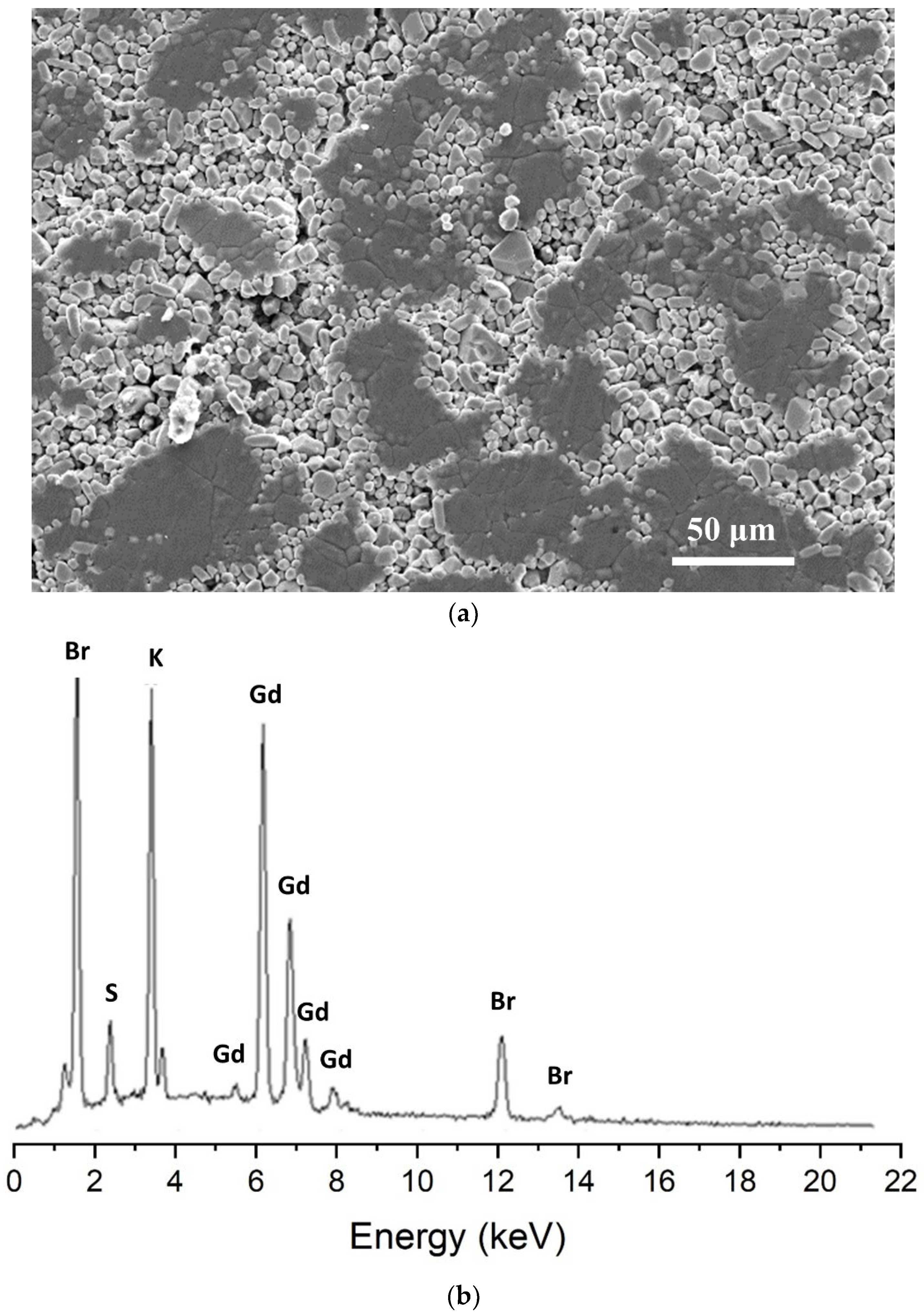
3.2. Scanning Electron Microscopy (SEM) and Microanalysis (EDS)

SEM observations of samples show substantially the same appearance of different pills. In Figure 4a, the morphological structure of the Gd2O2S screens is shown. Thanks to backscattered electrons used for acquisition, and local EDS analysis, brighter zones were identified as Gd2O2S and darker regions as KBr. Average grain size and non-optimized distribution of materials are noticeable in the image (Figure 4a). This inhomogeneity influences optical behavior, generating possible scattering, multiple reflections, and reabsorption of photons along complex optical paths.
EDS analysis, presented in Figure 4b, evidences the presence of Gd, S, Br, and K in all samples, while activator peaks are lost in the ground noise of the spectrum, probably due to low content with respect to the EDS sensitivity limit of 1%. Therefore, the EDS results show that dopant content is lower than 1% in all analyzed samples.

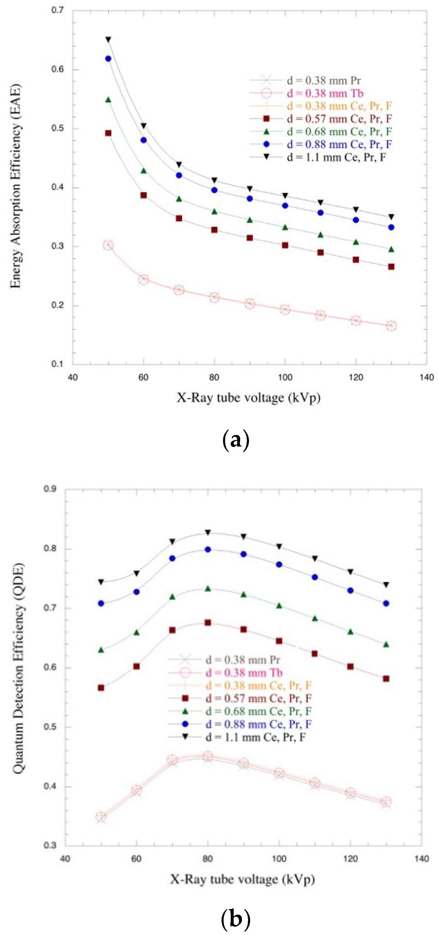
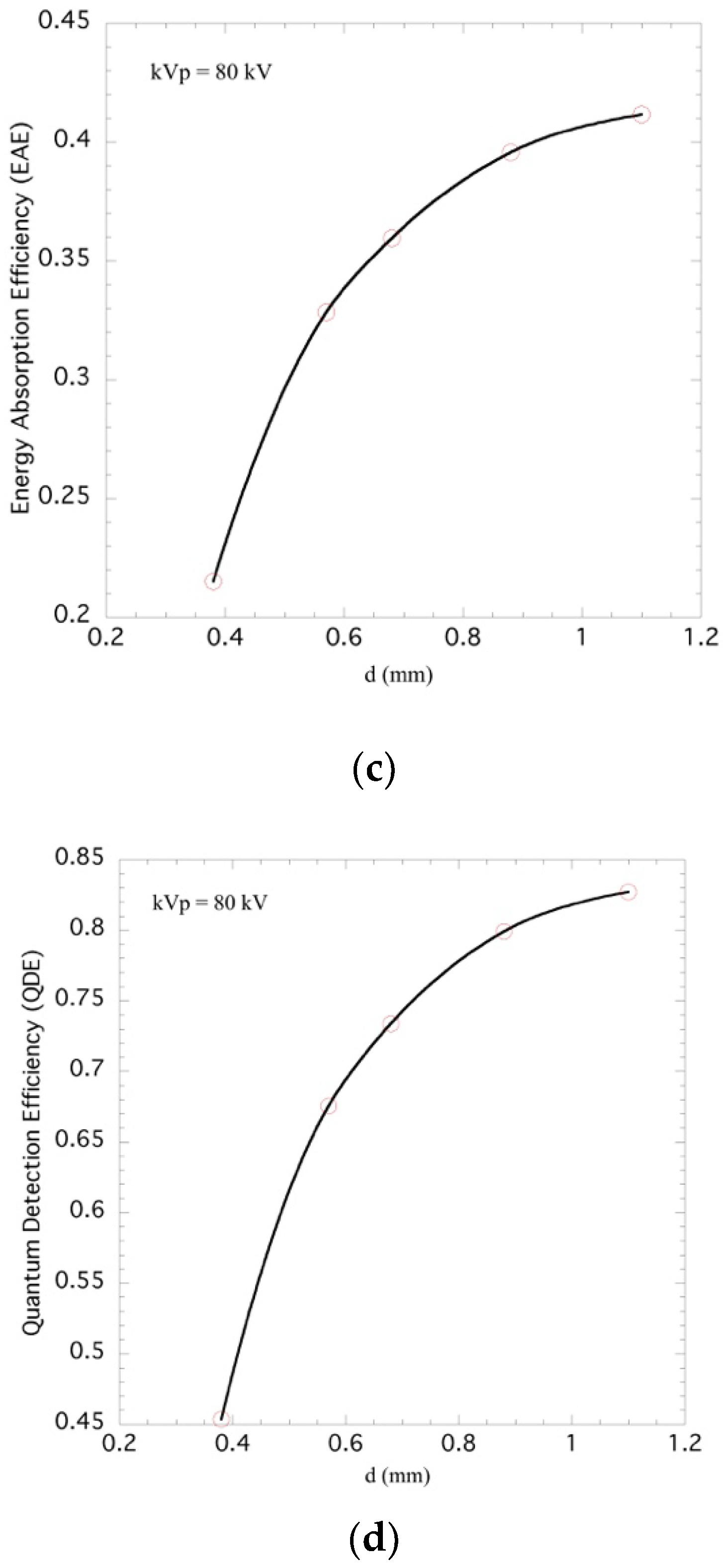
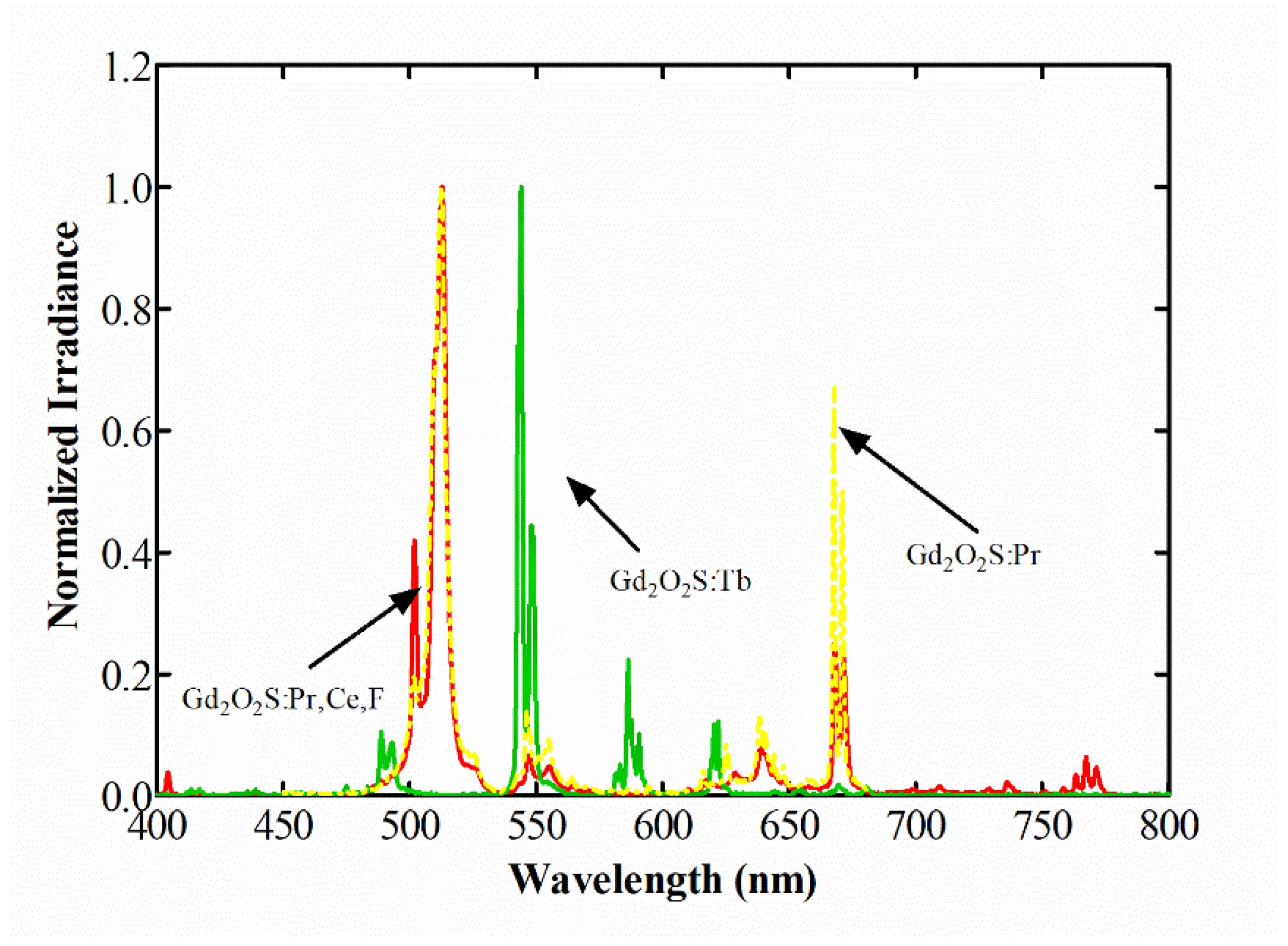
3.3. X-ray Detection Efficiency Parameters and Emission Properties of GOS Screens

In Figure 5a,b, variations of EAE and QDE with increasing X-ray tube voltages (from 50 to 130 kVp) are reported. All the curves follow the same trend, EAE decreases with X-ray tube voltage, as expected, and this behavior is not influenced by the dopant agent but only by the thickness of the screens. In Figure 5c, it is observable that the EAE increases with the increasing thickness of the screens. In fact, a lower value of EAE is obtained for the thinner Gd2O2S:Pr,Ce,F screen (0.38 mm). Higher values were obtained for the thicker one (1.1 mm). In all the Gd2O2S screens, the dominant effect is due to the mass and energy of the source, so the EAE seems to saturate as a function of thickness to higher values and as a function of energy toward lower values.
QDE increases until 80 kVp, and then it decreases for higher X-ray tube voltages (Figure 5b). This is due to the K-absorption energy edge of the gadolinium (Gd) element at 50.2 keV, which suddenly increases the X-ray absorption probability, allowing the generation of a relatively large number of K-fluorescence photons. The QDE values are higher than the EAE ones. This is due to the emerging K-fluorescence photons or scattered X-rays (Rayleigh or Compton scattering) that do not lead to local energy deposition and thus, are not included in the EAE calculations. The highest QDE value is presented for the 1.1 mm thick screen since its increased thickness enhances X-ray photon absorption (Figure 5d).
Figure 6 shows the optical photon emission spectra of Gd2O2S:Tb, Gd2O2S:Pr, and Gd2O2S:Pr,Ce,F scintillator samples under X-ray excitation. Analyzing the emission spectrum of the Gd2O2S:Tb screen, peaks are found between 475 nm and 550 nm (where the maximum is), as expected from the literature. The measured spectrum of Gd2O2S:Pr presents 2 distinct peaks at 512 nm and 668 nm, respectively. These peaks correspond to an average photon energy of 2.16 eV. From Figure 6, it can be seen that the Gd2O2S:Pr,Ce,F spectrum consists of a dominant line at 513 nm, lying in the green region of the optical spectrum, and 4 weaker peaks at 547, 640, 665, and 767 nm [33]. According to Rodnyĭ, the 5d→4f luminescence of Ce3+ ions cannot be the case in the Gd2O2S matrix since the corresponding 5d levels are within the conduction band. When any excited levels of a luminescence center fall in the conduction band, the emission is absent because of mixing with the conduction band states [34,35]. Thus, all the emission peaks are associated with 4f2–4f2 lines of Pr3+, since Ce3+ cannot be used as a luminescence center in the Gd2O2S matrix [33]. Having a maximum at 513 nm, the mean light photon energy (Eλ = hc/λ) results in 2.42 eV. Similar emission spectra were recorded from previously studied phosphor screens produced by a sedimentation technique [11,17,30].

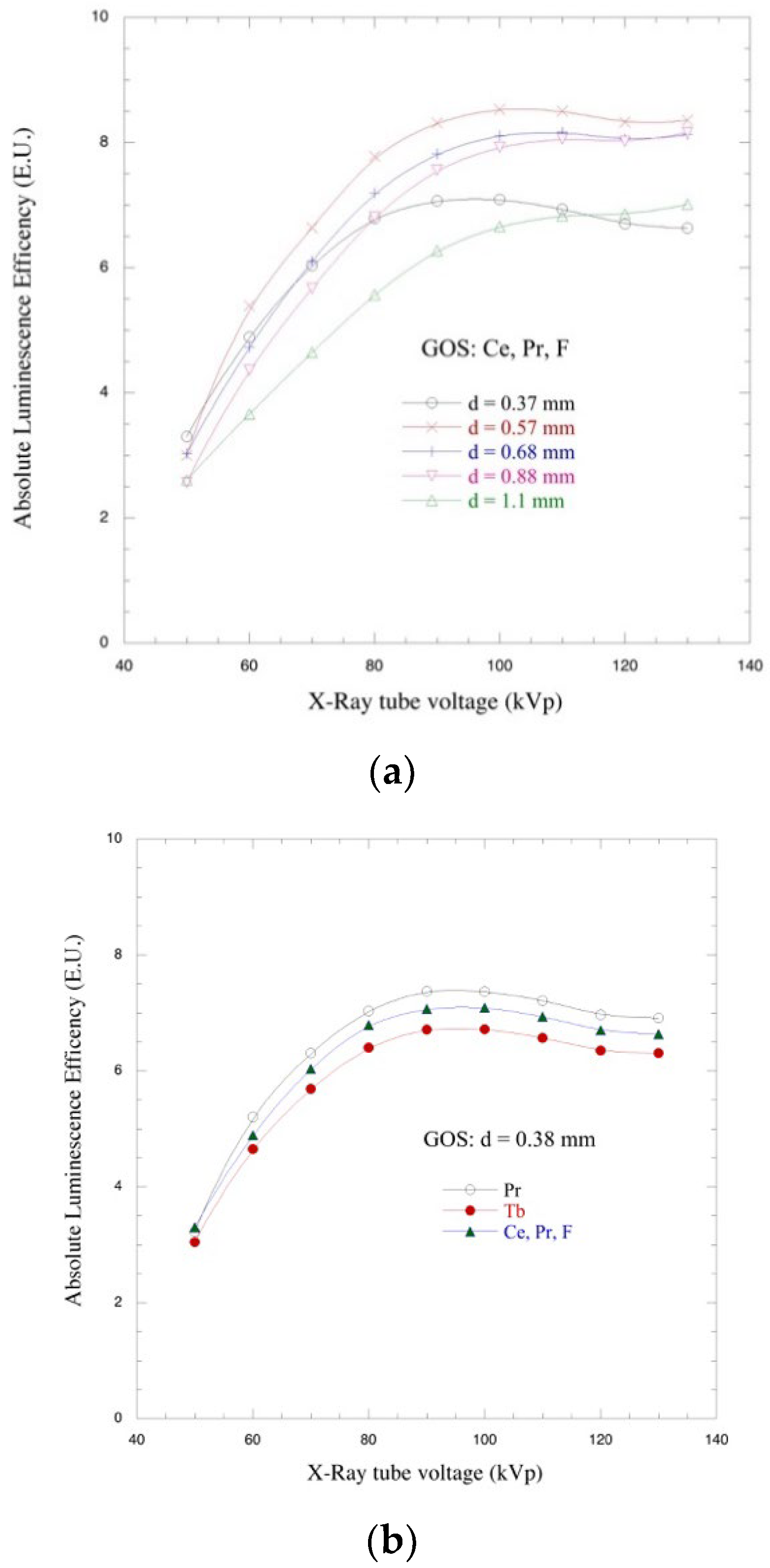
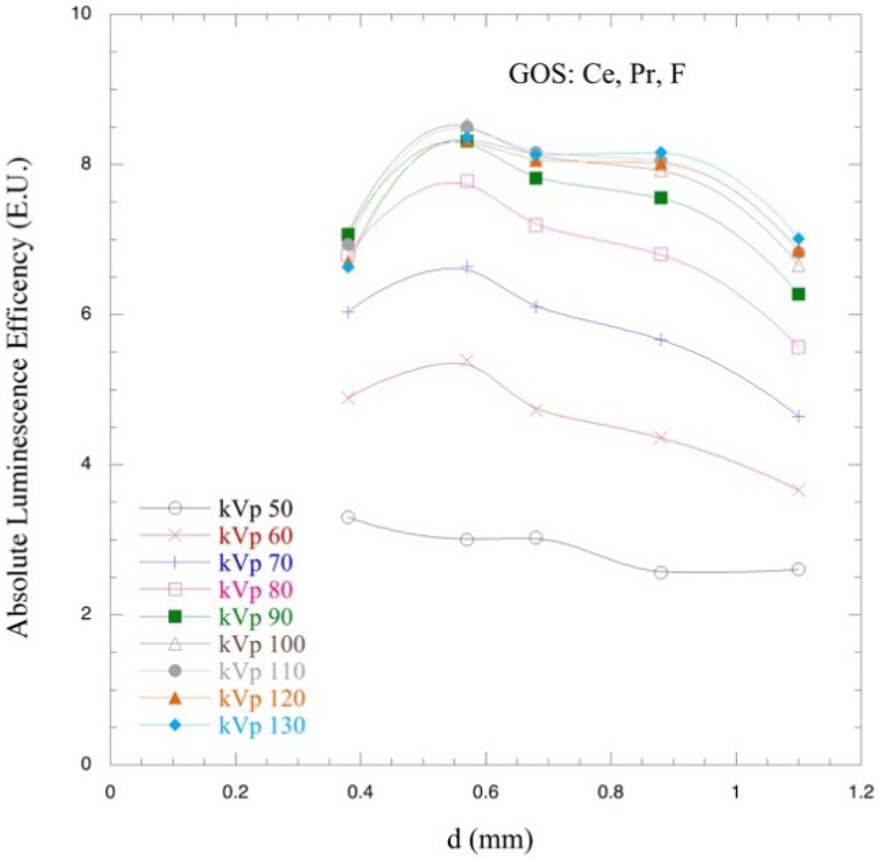
3.4. Absolute Luminescence Efficiency (ALE) of Gd2O2S Powder Screens

ALE seven powder screens (listed in Table 1) were investigated and experimentally valued. In Figure 7a,b, the ALE is reported as a function of X-ray tube voltages used in radiographic applications (50–130 kVp). The efficiency increases for all screens continuously with increasing X-ray tube voltage up to about 90–100 kVp. ALE curves show a tendency to saturate for higher X-ray tube voltages (100–130 kVp); the saturation proves that an excessive X-ray dose does not improve the luminescence efficiency. Among different thicknesses, the lowest value of ALE is exhibited by the thicker screen (1.1 mm), while the higher value of ALE is exhibited by the screen with 0.57 mm of thickness. Therefore, the trend is not linear (Figure 7a). Comparing powder screens doped with different materials (Figure 7b), the lower value of ALE is shown by the Gd2O2S:Tb screen, and the Pr doped appears to be the most efficient. This latter result seems to be in contrast with the literature; however, measurements were repeated a number of times with the same results. An investigation of the phenomenon is ongoing, exploring all the possible relations between structural conditions and performances.
Figure 8 illustrates the ALE of 5 GOS:Pr,Ce,F screens (0.38, 0.57, 0.68, 0.88, and 1.1 mm) as a function of thickness and X-ray tube voltages. For the 0.57 mm thick screen, the corresponding absolute efficiency maximum was observed at the X-ray tube voltage of 100 kVp. Screens thicker than ~0.8 mm seem to present lower scintillation light output in the whole kilovoltage range, mainly due to the semi-transparency and optical scattering characteristics of the screens. An explanation of this can be given by considering the extended distance—from the site of scintillation creation—that the optical photons have to propagate in the thicker GOS:Pr,Ce,F screen of, i.e., 1.1 mm, leading to optical photon loss inside the phosphor mass. In addition to the screen’s thickness, the optical photon losses are a function of the grain size, the optical photon energy, the index of refraction of the material, and errors in the detector’s manufacturing processes [22].

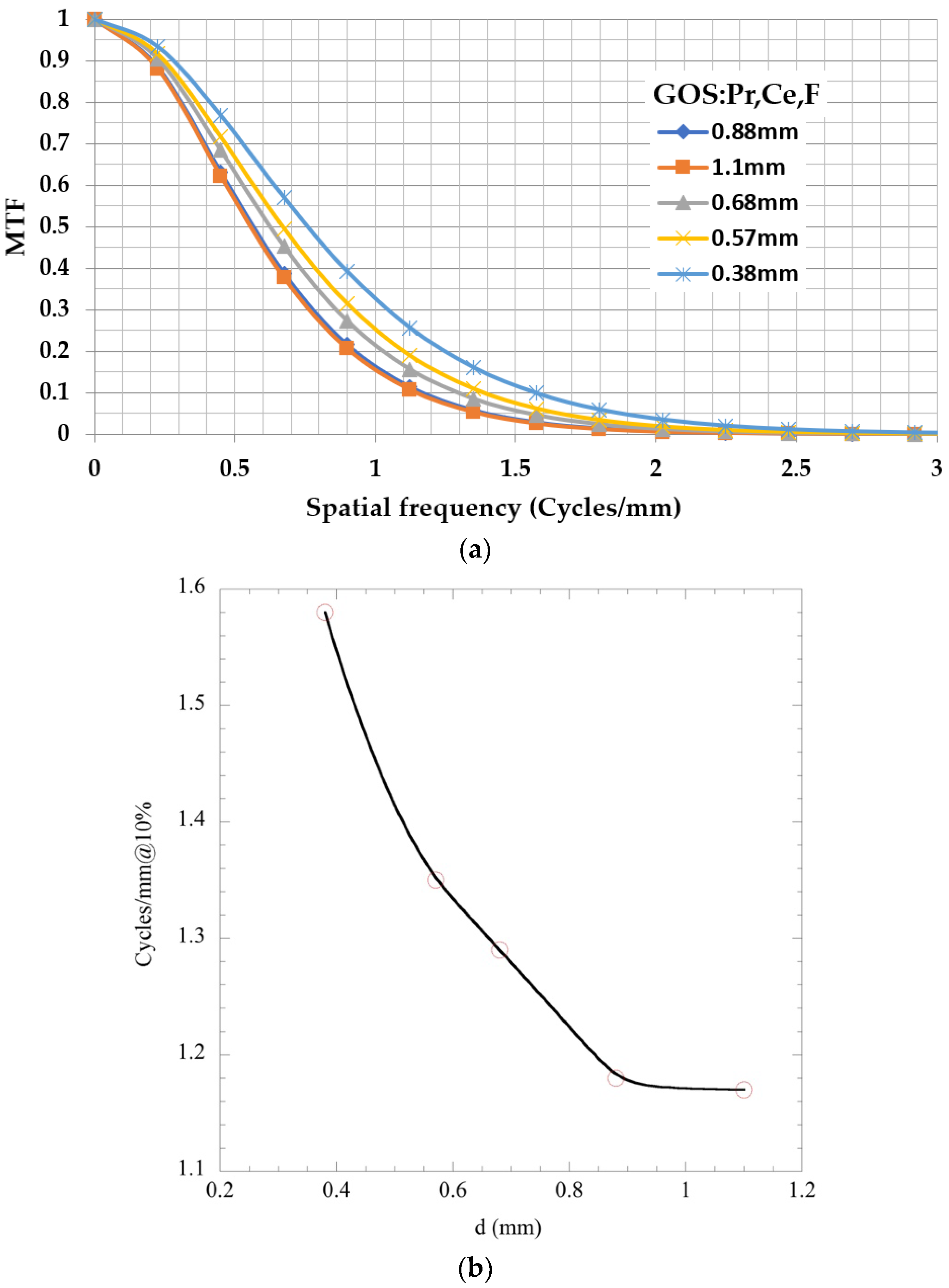
3.5. Modulation Transfer Function (MTF)

In Figure 9a, the MTF of the examined co-doped screens is reported. Here, the thinner 0.38 mm screen exhibits the highest resolution value (1.58 cycles/mm @ 10%), whereas, as the thickness of the screen increases, resolution degrades progressively. The corresponding values of the thicker screens are: 1.35 cycles/mm@10% for the 0.57 mm screen, 1.29 cycles/mm@10% for the 0.68 mm screen, 1.18 cycles/mm@10% for the 0.88 mm screen, and 1.17 cycles/mm@10% for the thicker 1.1 mm screen. It can be seen that the resolution loss is limited after the thickness of 0.88 mm since the 0.88 mm and the 1.1 mm screens appear with almost the same resolution properties (Figure 9a). The relatively low-resolution values are attributed to the thickness of the prepared samples. Thinner screens of similar Gd2O2S:Pr,Ce,F powder material (coating thickness of 35.7 mg/cm2) were found to have an MTF value of 4.2 cycles/mm@10% in previous studies [36]. The coating thickness of 35.7 mg/cm2 corresponds to a 97.27 µm thick screen, assuming a density of 7.34 g/cm3 and a 50% packing density. This thickness, which is almost 4 times less than the thinner sample prepared in this study, is considered typical for low-energy applications such as mammography, where commercial screens can be found with thicknesses of the order of 118.9 µm [37]. As the energy increases, thicker screens are used with thicknesses up to some millimeters. Figure 9b summarizes the MTF related to different thickness.

4. Conclusions

Gadolinium oxysulfide (Gd2O2S) scintillator ceramic screens, with several doping strategies (Tb3+, Ce3+, Pr3+, and F), have been investigated in terms of luminescence and imaging performance to assess their suitability for imaging purposes. Structural characterization was carried out to assess the quality and the purity of the compounds and possible correlations with the luminescence performances. In addition, four different thicknesses of the co-doped Gd2O2S (Pr,Ce,F) sample were studied to determine the influence of thickness on the luminescence and imaging parameters.
The structural investigation has revealed a good quality of the samples in terms of crystallinity. Despite their low detectability due to the low percentage in the compounds (<1%), the presence of the dopants is revealed by the changes in the XRD peak intensities, which are different from the reference ones for Gd2O2S nominal values. The structure factor is consistently affected by the presence of the impurities giving specific and different luminescence and optical properties to the compounds. The EDS analysis confirmed the presence of the main components, including KBr, while SEM observation highlights the non-optimized distribution of the compound over the sample volume generating a large spread of light leading to reabsorption and loss of light. A more repeatable and accurate preparation is needed for future tests. The emission spectra present a huge part in the green region for all the samples, with some red peaks, especially for the Pr single doped Gd2O2S. This latter part is largely suppressed in the co-doped scintillators. In any case, the emission spectra match the majority of the optical detectors.
The luminescence tests were carried out using an X-Ray tube voltage range typically used in general radiography and fluoroscopy, simulating a real medical examination environment, including a filter simulating the human body. The highest value of the absolute luminescence efficiency (ALE) among the samples with the same thickness was detected for the Praseodymium (Pr) doped Gd2O2S. The ALE efficiency is even higher for the 0.57 mm thicker co-doped GOS (Gd2O2S:Pr,Ce,F), while higher thicknesses do not have a positive influence on the ALE. This is probably due to the light spread and reabsorption inside the sample volume, which has a longer optical path. ALE increased with increasing X-ray energy, with a saturation value around 100 kVp, in the same manner for all the Gd2O2S samples.
The calculation of the modulation transfer function (MTF), which quantifies the spatial resolution of an imaging system, presents the best values on thinner screens.
All the analyzed screens are, however, possible candidates as good scintillation materials for radiography and dosimetry applications. Thicker screens are, in most cases, preferable to the thinner ones, presenting good EAE and QDE performances together with mechanical stability, while thinner ones have a good spatial resolution with higher MTF values. However, the maximum ALE value is at a thickness of 0.57 mm, which would be a good compromise between detection efficiency, light production, and resolution. Among the thinner screens, the Pr doped demonstrates the best ALE efficiency, results that suggest future tests on a Pr doped sample with 0.58 mm of thickness. The emission spectra of the co-doped samples seem to be more monochromatic, which in some cases could be more efficient for the optical coupling. Finally, it is crucial to underline that the 100 kVp is enough to maximize the performance in all the samples; no extra dose or exposure is needed.

Author Contributions

Conceptualization, L.M., G.F. and S.D.; methodology, A.D.M., D.R., P.M., L.M., S.D. and I.K.; software, N.M., V.K., C.M. and P.M.; validation, A.D.M., D.R., I.V., L.M., S.D. and A.B.; formal analysis, C.M.; investigation, A.D.M., D.R., P.M., L.M., S.D. and I.K.; resources, A.B., C.F. and P.M.; writing—original draft preparation, A.D.M., D.R., P.M., L.M. and S.D.; writing—review and editing, A.D.M., D.R., P.M., L.M., I.V., C.M., I.K. and S.D.; visualization, L.M., D.R., P.M. and S.D.; supervision, S.D. and L.S. All authors have read and agreed to the published version of the manuscript.

Funding

This research received no external funding.

Institutional Review Board Statement

Not applicable.

Informed Consent Statement

Not applicable.

Data Availability Statement

The data are presented in the manuscript; any other details about data or raw data must be requested to the authors.

Acknowledgments

The present work was partially developed during an Erasmus Plus Traineeship program between the Department of Biomedical Engineering of the University of West Attica, Greece (Athens) and the Università Politecnica delle Marche, Italy (Ancona).

Conflicts of Interest

The authors declare no conflict of interest.

References

  1. Nikl, M. Scintillation detectors for X-rays. Meas. Sci. Technol. 2006, 17, R37. [Google Scholar] [CrossRef]
  2. Blasse, G.G.; Grabmaier, B.C. Luminescent Materials; Springer: Berlin/Heidelberg, Germany, 1994. [Google Scholar]
  3. Van Eijk, C.W.E. Inorganic scintillators in medical imaging. Phys. Med. Biol. 2002, 47, R85. [Google Scholar] [CrossRef] [PubMed]
  4. Van Eijk, C.W.E. Radiation detector developments in medical applications: Inorganic scintillators in positron emission tomography. Radiat. Prot. Dosim. 2008, 129, 13–21. [Google Scholar] [CrossRef] [PubMed]
  5. Del Guerra, A. Ionizing Radiation Detectors for Medical Imaging; World Scientific Publishing Co., Inc.: Singapore, 2004; ISBN 9812386742. [Google Scholar]
  6. Boone, J.M. Handbook of Medical Imaging: Physics and Psycophysics; Beutel, J., Kundel, H.L., Van Metter, R.L., Eds.; SPIE Press: Bellingham, WA, USA, 2000; Volume 1, pp. 36–57. [Google Scholar]
  7. Liaparinos, P.; Kalyvas, N.; Katsiotis, E.; Kandarakis, I. Investigating the particle packing of powder phosphors for imaging instrumentation technology: An examination of Gd2O2S:Tb phosphor. J. Instrum. 2016, 11, P10001. [Google Scholar] [CrossRef]
  8. Greskovich, C.; Duclos, S. Ceramic scintillators. Annu. Rev. Mater. Sci. 1997, 27, 69–88. [Google Scholar] [CrossRef]
  9. Yanagida, T.; Kamada, K.; Fujimoto, Y.; Yagi, H.; Yanagitani, T. Comparative study of ceramic and single crystal Ce: GAGG scintillator. Opt. Mater. 2013, 35, 2480–2485. [Google Scholar] [CrossRef]
  10. Park, C.; Kim, C.; Kim, J.; Lee, Y.; Na, Y.; Lee, K.; Yeom, J.Y. Performance comparison between ceramic Ce:GAGG and single crystal Ce:GAGG with digital-SiPM. J. Instrum. 2017, 12, P01002. [Google Scholar] [CrossRef]
  11. Yamada, H.; Suzuki, A.; Uchida, Y.; Yoshida, M.; Yamamoto, H. A Scintillator Gd2O2S:Pr, Ce, F for X-ray Computed Tomography. J. Electrochem. Soc. 1989, 136, 2713. [Google Scholar] [CrossRef]
  12. Zhigang, S.; Bin, L.; Guiping, R.; Hongbing, C. Synthesis of Green-Emitting Gd2O2S:Pr3+ Phosphor Nanoparticles and Fabrication of Translucent Gd2O2S:Pr3+ Scintillation Ceramics. Nanomaterials 2020, 10, 1639. [Google Scholar] [CrossRef]
  13. Blahuta, S.; Viana, B.; Bessière, A. Luminescence quenching processes in Gd2O2S:Pr3+, Ce3+ scintillating ceramics. Opt. Mater. 2011, 33, 1514–1518. [Google Scholar] [CrossRef]
  14. David, S.; Michail, C.; Seferis, I.; Valais, I.; Fountos, G.; Liaparinos, P.; Kandarakis, I.; Kalyvas, N. Evaluation of Gd2O2S:Pr granular phosphor properties for X-ray mammography imaging. J. Lumin. 2016, 169, 706–710. [Google Scholar] [CrossRef]
  15. Dezi, A.; Monachesi, E.; D’Ignazio, M.; Scalise, L.; Montalto, L.; Paone, N.; Rinaldi, D.; Mengucci, P.; Loudos, G.; Bakas, A.; et al. Structural Characterization and Absolute luminescence Efficiency Evaluation of Gd2O2S Highly Packing Density Ceramic Screens Doped with Tb3+ and Eu3+ for further Applications in Radiology. J. Phys. Conf. Ser. 2017, 931, 012029. [Google Scholar] [CrossRef]
  16. Michail, C.; Valais, I.; Martini, N.; Koukou, V.; Kalyvas, N.; Bakas, A.; Kandarakis, I.; Fountos, G. Determination of the detective quantum efficiency (DQE) of CMOS/CsI imaging detectors following the novel IEC 62220-1-1:2015 International Standard. Radiat. Meas. 2016, 94, 8–17. [Google Scholar] [CrossRef]
  17. Montalto, L.; Natali, P.P.; Daví, F.; Mengucci, P.; Paone, N.; Rinaldi, D. Characterization of a defective PbWO4 crystal cut along the a-c crystallographic plane: Structural assessment and a novel photoelastic stress analysis. J. Instrum. 2017, 12, P12035. [Google Scholar] [CrossRef] [Green Version]
  18. Montalto, L.; Natali, P.P.; Scalise, L.; Paone, N.; Davì, F.; Rinaldi, D.; Barucca, G.; Mengucci, P. Quality control and structural assesment of anisotropic scintillating crystals. Crystals 2019, 9, 376. [Google Scholar] [CrossRef] [Green Version]
  19. Pavia, D.L.; Lampman, G.M.; Kriz, G.S.; Vyvyan, J.A. Introduction to Spectroscopy, 3rd ed.; Brooks/Cole Cengage Learning: Boston, MA, USA, 2009. [Google Scholar]
  20. Saeed, K.A.; Fartosy, S.H. Using Infrared Spectroscopy to Examine the Influences of Stabilizers on the Molecular Structure of Stabilized Contaminated Clay Soils. In Geotechnical Engineering and Sustainable Construction; Karkush, M.O., Choudhury, D., Eds.; Springer: Singapore, 2022; pp. 781–791. [Google Scholar]
  21. Michail, C.; Valais, I.; Seferis, I.E.; Kalyvas, N.; David, S.; Fountos, G.; Kandarakis, I. Measurement of the luminescence properties of Gd2O2S:Pr,Ce,F powder scintillators under X-ray radiation. Radiat. Meas. 2014, 70, 59–64. [Google Scholar] [CrossRef]
  22. Seferis, I.E.; Michail, C.M.; Valais, I.G.; Zeler, J.; Liaparinos, P.; Fountos, G.; Kalyvas, N.; David, S.; Stromatia, F.; Zych, E.; et al. Light emission efficiency and imaging performance of Lu2O3:Eu nanophosphor under X-ray radiography conditions: Comparison with Gd2O2S:Eu. J. Lumin. 2014, 151, 229–234. [Google Scholar] [CrossRef]
  23. Michail, C.; Fountos, G.; Liaparinos, P.; Kalyvas, N.; Valais, I.; Kandarakis, I.S.; Panayiotakis, G.S. Light emission efficiency and imaging performance of Gd2O2S:Eu powder screens under X-ray radiography conditions. Med. Phys. 2010, 37, 3694–3703. [Google Scholar] [CrossRef]
  24. Boone, J.M. X-ray production, interaction, and detection in diagnostic imaging. In Handbook of Medical Imaging: Physics and Psycophysics, 1st ed.; Beutel, J., Kundel, H.L., Van Metter, R.L., Eds.; SPIE Press: Bellingham, WA, USA, 2000; p. 40. [Google Scholar]
  25. Yaffe, M.J.; Rowlands, J.A. X-ray detectors for digital radiography. Phys. Med. Biol. 1997, 42, 1–39. [Google Scholar] [CrossRef]
  26. Nowotny, R. XMuDat: Photon Attenuation Data on PC (IAEA-NDS-195); International Atomic Energy Agency: Vienna, Austria, 1998. [Google Scholar]
  27. Michail, C.; Kalyvas, N.; Valais, I.; David, S.; Seferis, I.; Toutountzis, A.; Karabotsos, A.; Liaparinos, P.; Fountos, G.; Kandarakis, I. On the response of GdAlO3:Ce powder scintillators. J. Lumin. 2013, 144, 45–52. [Google Scholar] [CrossRef]
  28. David, S.; Michail, C.; Valais, I.; Toutountzis, A.; Cavouras, D.; Kandarakis, I.; Panayiotakis, G. Investigation of luminescence properties of Lu2SiO5:Ce (LSO) powder scintillator in the Χ-ray radiography energy range. ΙΕΕΕ Trans. Nucl. Sci. 2008, 55, 6. [Google Scholar]
  29. David, S.L.; Michail, C.M.; Roussou, M.; Nirgianaki, E.; Toutountzis, A.E.; Valais, I.G.; Fountos, G.; Liaparinos, P.F.; Kandarakis, I.; Panayiotakis, G. Evaluation of the luminescence efficiency of YAG:Ce powder scintillating screens for use in digital mammography detector. ΙΕΕΕ Trans. Nucl. Sci. 2010, 57, 951–957. [Google Scholar] [CrossRef]
  30. Michail, C.M.; Fountos, G.P.; David, S.L.; Valais, I.G.; Toutountzis, A.E.; Kalyvas, N.E.; Kandarakis, I.S.; Panayiotakis, G.S. A comparative investigation of Lu2SiO5:Ce and Gd2O2S:Eu powder scintillators for use in Χ-ray mammography detectors. Meas. Sci. Technol. 2009, 20, 104008. [Google Scholar] [CrossRef]
  31. Kalyvas, N.; Liaparinos, P.; Michail, C.; David, S.; Fountos, G.; Wójtowich, M.; Zych, E.; Kandarakis, I. Studying the luminescence efficiency of Lu2O3:Eu nanophosphor material for digital X-ray imaging applications. Appl. Phys. A 2012, 106, 131–136. [Google Scholar] [CrossRef]
  32. IEC 62220-1-1; Medical Electrical Equipment-Characteristics of Digital X-ray Imaging Devices—Part 1-1: Determination of the Detective Quantum Efficiency-Detectors Used in Radiographic Imaging. IEC—International Electrotechnical Commission: Geneva, Switzerland, 2015.
  33. Wang, W.; Kou, H.; Liu, S.; Shi, Y.; Li, J.; Li, Y.; Feng, X.; Pan, Y.; Guo, J. Comparison of the Optical and Scintillation Properties of Gd2O2S:Pr, Ce Ceramics Fabricated by Hot Pressing and Pressureless Sintering. Opt. Mater. 2015, 42, 199–203. [Google Scholar] [CrossRef]
  34. Rodnyĭ, P.A. Energy Levels of Rare-Earth Ions in Gd2O2S. Opt. Spectrosc. 2009, 107, 270–274. [Google Scholar] [CrossRef]
  35. Yen, W.M.; Jia, D.; Lu, L.; Meltzer, R.S. Two-Step Photoconductivity: Determination of Impurity Levels of Er3+ Relative to the Host Bands of Gd2O3. J. Lumin. 2003, 102–103, 333–337. [Google Scholar] [CrossRef]
  36. Michail, C. Image Quality Assessment of a CMOS/Gd2O2S:Pr,Ce,F X-Ray Sensor. J. Sens. 2015, 2015, 874637. [Google Scholar] [CrossRef] [Green Version]
  37. Michail, C.; Valais, I.; Fountos, G.; Bakas, A.; Fountzoula, C.; Kalyvas, N.; Karabotsos, A.; Sianoudis, I.; Kandarakis, I. Luminescence efficiency of calcium tungstate (CaWO4) under X-ray radiation: Comparison with Gd2O2S:Tb. Measurement 2018, 120, 213–220. [Google Scholar] [CrossRef]
Figure 1. X-ray energy fluence spectra ( Ψ 0 ) produced at 70, 100, and 130 kVp.
Crystals 12 00854 g001
Figure 2. Experimental setup for the measurement of the emitted light energy flux comprising the integrating sphere, the PMT, and the vibrating reed electrometer.
Crystals 12 00854 g002
Figure 3. XRD patterns of GOS screens doped with different activators. Miller indices are reported for peaks of the Gd2O2S compound. The unindexed peaks are due to KBr.
Crystals 12 00854 g003
Figure 4. (a) SEM image of Gd2O2S screens showing the distribution of Gd2O2S (brighter regions) and KBr (darker regions) compounds. (b) EDS micro-analysis spectrum detecting main elements composing screens.
Crystals 12 00854 g004
Figure 5. (a) Energy absorption efficiency (EAE) of Gd2O2S powder screens as a function of X-ray tube voltages. (b) Quantum detection efficiency (QDE) of Gd2O2S powder screens as a function of X-ray tube voltages. Points correspond to calculated values (from 50 kVp to 130 kVp). All screens with the same thickness d = 0.38 mm gave the same results, so the points in the figure are superimposed. (c) Energy absorption efficiency (EAE) as a function of the thickness. (d) Quantum detection efficiency (QDE) as a function of the thickness. The solid lines in the graphs are guides for the eyes.
Crystals 12 00854 g005aCrystals 12 00854 g005b
Figure 6. In the emission spectrum we can recognize the Gd2O2S:Tb screen with its main peaks at 475 nm and 550 nm; the Gd2O2S:Pr screen with its main peaks at 512 nm and 668 nm; and the Gd2O2S:Pr,Ce,F screen with its max peak at 513 nm.
Crystals 12 00854 g006
Figure 7. (a) Absolute luminescence efficiency (ALE) of Gd2O2S:Pr,Ce,F powder screens with different thicknesses and same dopant agents. (b) ALE of Gd2O2S powder screens with different dopants and same thickness. The vertical axis units are E.U. values (1 E.U equal to μW m−2/ mR s−1). The solid lines in the graphs are guides for the eyes.
Crystals 12 00854 g007
Figure 8. The ALE as a function of thickness for GOS:Pr,Ce,F for different X-ray tube voltages. The solid lines in the graphs are guides for the eyes.
Crystals 12 00854 g008
Figure 9. (a) Comparison of the MTFs of Gd2O2S:Pr,Ce,F employed in the Kodak Min-R screens as measured experimentally in transmission mode 1 cycle mm−1 = 1 lp mm−1. (b) cycles/mm@10% of Gd2O2S:Pr,Ce,F as a function of the screens’ thickness. The solid line in the graphs is a guide for the eyes.
Crystals 12 00854 g009
Table 1. List of samples in the form of pills produced with different dopants and thicknesses.
SampleDopantThickness
(mm)
PIL 1-#S1Pr0.38
PIL 5-#S2Tb0.38
PIL 2-#M1Pr, Ce, F0.38
PIL 10-#M2Pr, Ce, F0.57
PIL 9-#M3Pr, Ce, F0.68
PIL 7-#M4Pr, Ce, F0.88
PIL 8-#M5Pr, Ce, F1.1
#S1, #S2 and #M powders: Purchased from Phosphor Technology Ltd., Norton, UK.
Table 2. Experimental lattice parameters of the hcp Gd2O2S compound as estimated from peak shape analysis of XRD patterns. Nominal values are reported for comparison.
Lattice Parameters#S1#S2#M2Reference Value
a (nm)0.38487 ± 0.000110.38485 ± 0.000140.38487 ± 0.000130.3852
c (nm)0.6664 ± 0.00030.6665 ± 0.00040.6664 ± 0.00070.6670
Table 3. Relative intensity of Gd2O2S peaks in the angular range 2θ = 24°–42°. Reference values from ICDD file n. 26-1422 are reported for comparison.
Miller Indices (hkl)#S1#S2#M2Reference Value
(100)71303035
(101)100100100100
(102)32330
(003)181096
Publisher’s Note: MDPI stays neutral with regard to jurisdictional claims in published maps and institutional affiliations.

