Article

Achievement of Unidirectional Aluminum Tin Oxide/UV-Curable Polymer Hybrid Film via UV Nanoimprinting Lithography for Uniform Liquid Crystal Alignment

IT Nano Electronic Device Laboratory, Department of Electrical and Electronic Engineering, Yonsei University, 50 Yonsei-ro, Seodaemun-gu, Seoul 120-749, Korea
*
Author to whom correspondence should be addressed.
Crystals 2022, 12(6), 855; https://doi.org/10.3390/cryst12060855
Submission received: 26 May 2022 / Revised: 13 June 2022 / Accepted: 15 June 2022 / Published: 17 June 2022

Abstract

:
A uniform unidirectional nanostructure composed of aluminum tin oxide and ultraviolet (UV)-curable polymer is introduced herein. The nanostructure was produced by UV-nanoimprint lithography (UV-NIL), and the fabricated hybrid film was used as a uniform liquid crystal (LC) alignment layer. Atomic force microscopy and line profile analysis were performed to confirm a well-ordered nanostructure with 760 nm periodicity and 30 nm height. X-ray photoelectron spectroscopy analysis was also conducted to examine the chemical modifications to the hybrid film surface during UV exposure. Optical transmittance investigation of the nanopatterned hybrid film revealed its compatibility for LC device application. Stable, uniform, and homogeneous LC alignment on the hybrid film was confirmed by polarized optical microscopy observance and analysis of LC pretilt angle. The unidirectional structure on the film surface enabled uniform LC orientation along with surface anisotropy property. Hence, we expect that the proposed UV-NIL process can be applied to fabricate high-resolution unidirectional nanostructures with various inorganic/organic hybrid materials and that these nanostructures have high potential for next-generation LC systems.

1. Introduction

With the development of electron devices in recent times, the demand for high-technology display devices has also increased. Liquid crystal displays (LCDs) have various advantages, such as long-term durability, high resolution, and well-developed production procedures, and have been researched for several decades [1,2,3,4]. Liquid crystals (LCs) are the core material of the LCD. They have unique characteristics of refractive and dielectric anisotropies [5,6]. They are in an intermediate state between a solid and liquid, and show collective behavior characteristic with elastic properties [7]. Because of these distinct properties, LCs have been used in various fields, including chemistry [8,9], optics [10], and electronics [11]. Uniform LC alignment is one of the most important techniques in advanced LCD applications, which allows perfect light controllability. The alignment state of the LC molecules is affected chemically and physically by interactions between the alignment layer and LCs [12,13].
To achieve uniform LC alignment, many treatments to the alignment layer have been researched, such as the rubbing [14,15], sputtering [16], oblique evaporation [17], and photo-alignment [18,19,20,21,22] methods. In particular, the rubbing method has been conventionally adopted in industrial processes, where a rotating fabric roller is used to produce microgrooves on the surface of the alignment layer [23]. These microgrooves induce surface anisotropy and achieve unidirectional LC orientation. However, this method has several problems, such as dust, cracks, and contamination generation as well as electrostatic issues originating from mechanical contact between the fabric roller and alignment layer [24,25]. These problems can worsen the performances of devices. Other methods also have problems in terms of large-area processes and cost-effectiveness.
The ultraviolet (UV) nanoimprint lithography (NIL) method is generally adopted to imprint unidirectional nanopatterns on a target layer. We considered that such unidirectional nanopatterns could be utilized to align LCs uniformly with surface anisotropic characteristics. The unidirectional nanopatterns can guide LC orientation and achieve uniform LC alignment [26,27,28]. This method also has advantages, such as repeatability (fabricated mold can be continuously used to transfer nanopatterns to the alignment layer), high throughput, cost effectiveness, convenience (fewer process steps), and low-temperature processing [29,30].
The initial nanopattern was constructed on a silicon (Si) wafer via laser interference lithography (LIL), which is characterized by a maskless, fast process and can be applied to large-area processes. This nanopattern was then shifted to a polydimethylsiloxane (PDMS) sheet to be used as a master mold during the UV-NIL process. The hybrid mixture of aluminum tin oxide (AlSnO) and UV-curable polymer was used as the LC alignment layer. The AlSnO material was adopted because of its high optical transmittance and dielectric characteristics, which are important factors for LC device applications [31,32,33]. The AlSnO/UV-curable polymer mixed hybrid film was fabricated by the spin-coating method. Subsequently, the UV-NIL process was used to transfer the PDMS master mold nanopattern to the hybrid film. The atomic force microscopy (AFM) and corresponding line profile data were analyzed to examine the UV-nanoimprinted hybrid film surface morphology. The chemical property changes of the hybrid film based on UV exposure time were investigated by X-ray photoelectron spectroscopy (XPS). Optical transmittance was measured to evaluate the performance of hybrid film for LC system. The LC alignment state on the hybrid film was confirmed by observance of polarized optical microscopy (POM) and analysis of LC pretilt angle via crystal rotation method [34,35].

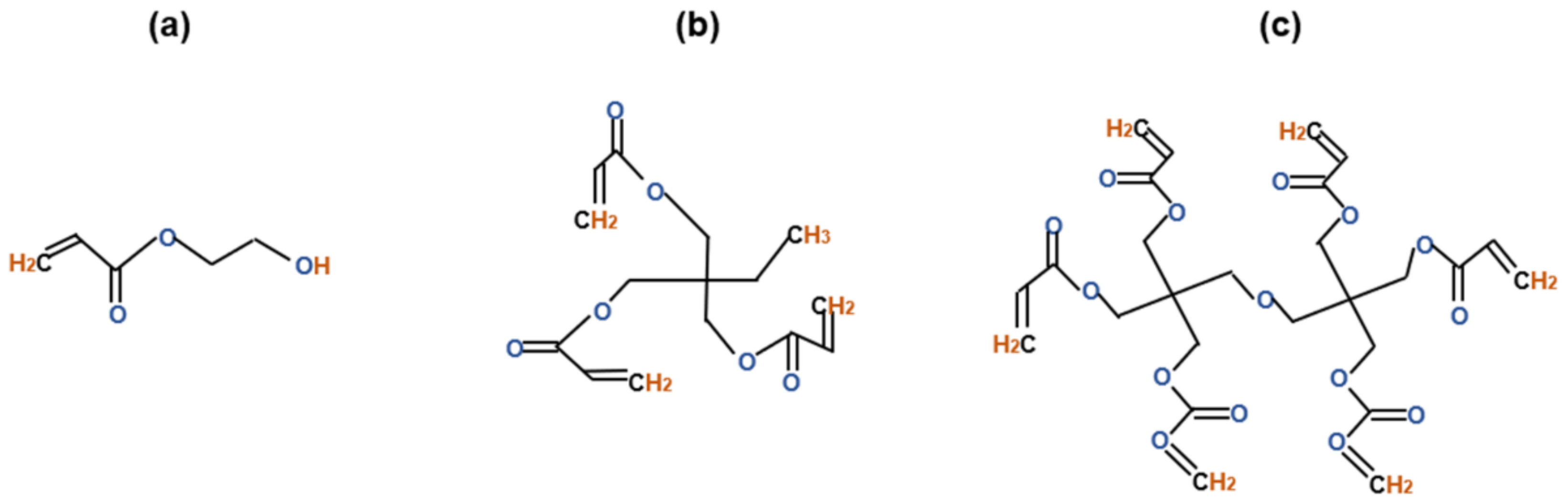
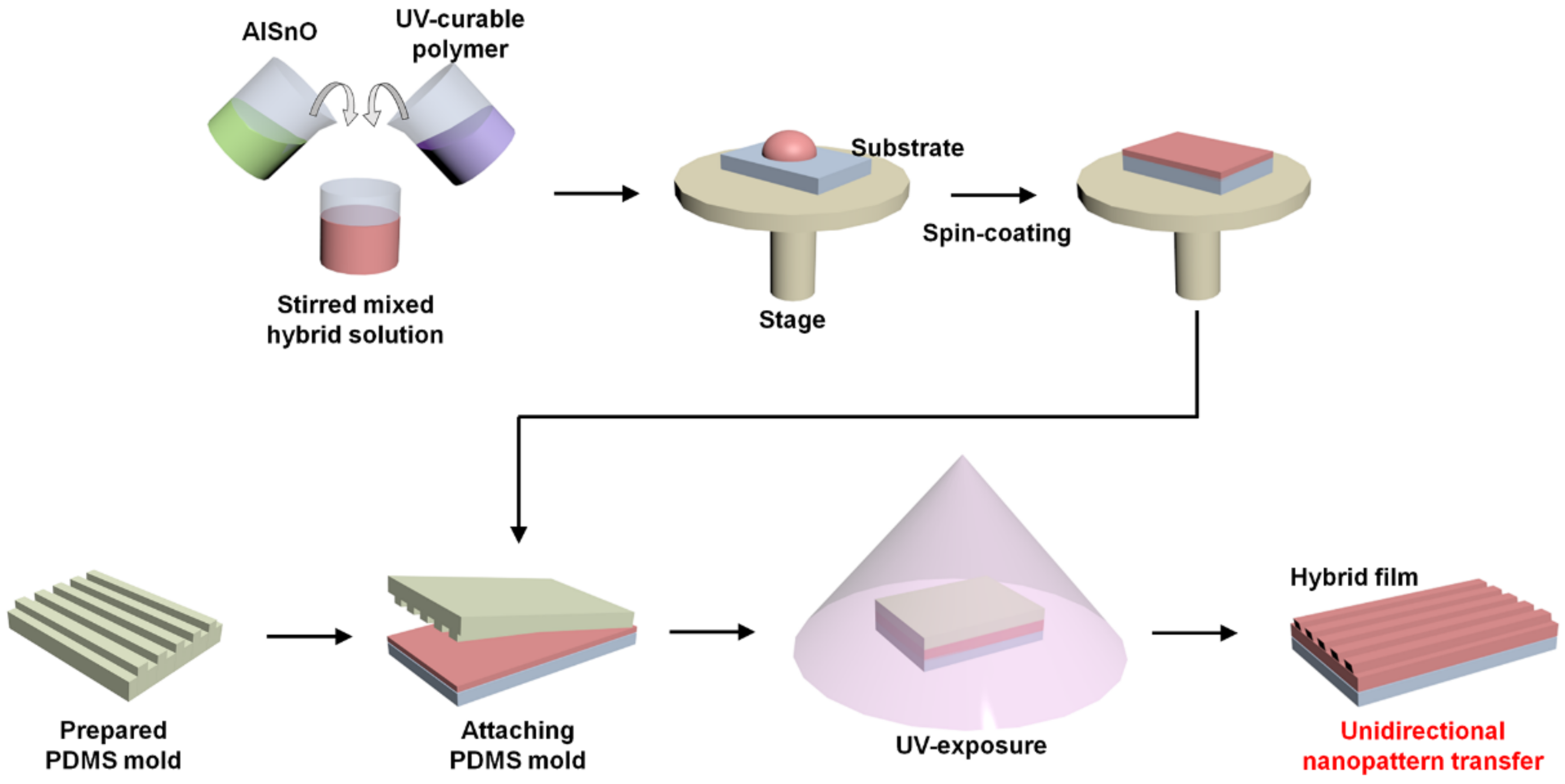
2. Materials and Methods

The initial nanoscaled uniform unidirectional structure was constructed on a Si wafer via the deep UV-LIL process. For the periodic nanostructure, an interferometer of single-beam Lloyd’s mirror and a 257 nm Ar laser were used. The Ar laser beam was amplified by 27 times for uniformity of dose, and the spatial frequency noise was removed with a pinhole. Thereafter, the continuously emitted coherent light was arrived at the Lloyd’s mirror and Si wafer. The reflected light created a one-dimensional nanostructure on the Si wafer surface. However, to ensure a conformal and continuous NIL process, the hard Si wafer pattern was transferred to a rigiflex mold, such as PDMS. The PDMS was produced by mixing a silicone elastomer base with a curing agent (SYLGARD 184, Dowhitech Corp., Goyang-si, Korea) in a 10:1 ratio. For the nanopattern transfer, the PDMS mixture was poured over the Si wafer and placed in a vacuum chamber to eliminate any bubbles or defects. The mixture was cured for 1 h at 75 °C, and the uniform unidirectional nanopattern was successfully transferred to the PDMS mold.
The 0.1 M UV-curable polymer composed of dipentaerythritol hexaacrylate (DPHEA), tripropyleneglycol diacrylate (TPGDA), and 2-hydroxyethyl acrylate (2HEA) in equal ratios was mixed with the UV photocuring agent (Irgacure 2959; Sigma-Aldrich, St. Louis, MI, USA, Ciba). 2HEA is helpful in advanced coating applications and contains a hydroxyfunctional acrylic monomer [36]. TPGDA is generally utilized for UV film formulations gelation stability at ambient temperatures because of its fast curing and low viscosity, and it contains a trifunctional monomer [37,38,39]. DPHEA is generally used for transparent antistatic hard coatings and contains a hexafunctional monomer [40]. The chemical structures of these polymer materials are shown in Figure 1. The 0.1 M AlSnO solution was fabricated by dissolving aluminum nitrate nonahydrate and tin (II) chloride in 2-methoxyethanol in equal ratios. Then, the mixture was stirred with a rate of 420 rpm at 80 °C for 2 h, followed by aging for 1 day to prepare the solution. The fabricated AlSnO solution was next mixed with the prepared UV-curable polymer in a 9:1 ratio and stirred with a rate of 420 rpm at ambient temperature (about 20 °C) for 1 h. Thus, the AlSnO/UV-curable polymer hybrid solution was obtained.
As a substrate of hybrid film, the 2 × 3 cm sized plain glasses were prepared, which involved cleaning by isopropyl alcohol and acetone for 10 min each by ultrasonication to remove any impurities. Thereafter, the substrates were rinsed with deionized water and subsequently dried using N2 gas. The produced hybrid solution was spin-coated on the substrate for 30 s at a rate of 3000 rpm. The fabricated PDMS mold was attached to the surface of coated film and it was moved for UV-beam exposure. A 365 nm UV beam was irradiated on the fabricated samples for 1 min, 3 min, and 6 min each. With the mercury lamp of 1 kW, the 7.9 mW/cm2 density of energy was kept during UV irradiation. The hybrid film was cured while forming the transferred nanopattern from the PDMS mold through the UV-NIL process. Lastly, attached PDMS mold was peeled off from the hybrid film with the shifting of one-dimensional nanostructure to that film surface. The AlSnO/UV-curable polymer hybrid solution production and nanopattern transfer via the UV-NIL process are presented in Figure 2.
The surface morphological information of the UV-nanoimprinted hybrid films was confirmed by AFM (XE-BIO, Park Systems, Suwon-si, Korea). The feature size of the UV-nanoimprinted structure was measured by AFM and line profiles. The nanopatterned PDMS mold was also observed for comparison. The stoichiometric characteristics of the hybrid films were investigated by XPS measurement (K-alpha, Thermo Fisher Scientific, Waltham, MA, USA). A monochromatic Al X-ray source (Al Ka line: 1486.6 eV) and a 12 kV/3 mA power source were used. The optical transmittance values of the hybrid films were observed by UV-Vis-NIR spectroscopy (JASCO Corporation, Tokyo, Japan, V-650) in the wavelength range of 250–850 nm.
To examine the applicability of the UV-nanoimprinted hybrid films as LC alignment layers, antiparallel (AP) cells were fabricated with a uniform 60 μm cell gaps. The nematic positive LCs (IAN-5000XX T14, ne = 1.595, no = 1.484, Δn = 0.111; JNC, Seongnam-si, Korea) were put into the between alignment layers with parallel direction of nanostructure via capillary force using a syringe. The quality of LC alignment on that layer was confirmed by POM observance (BXP 51, Olympus, Tokyo, Japan). The LC pretilt angle in the assembled AP-LC cell was analyzed using the crystal rotation method (Autronic TBA 107, Kashiwa, Japan).

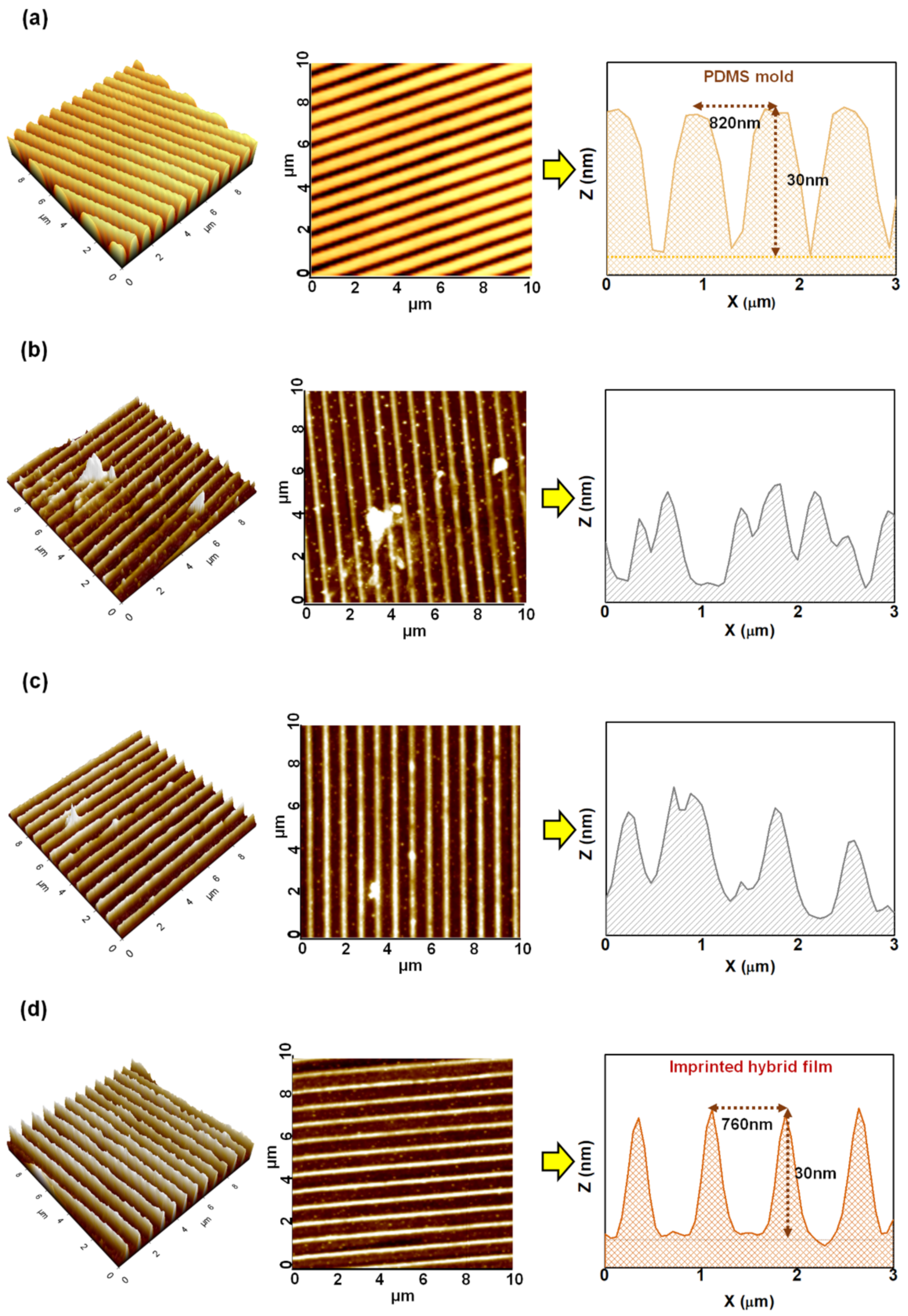
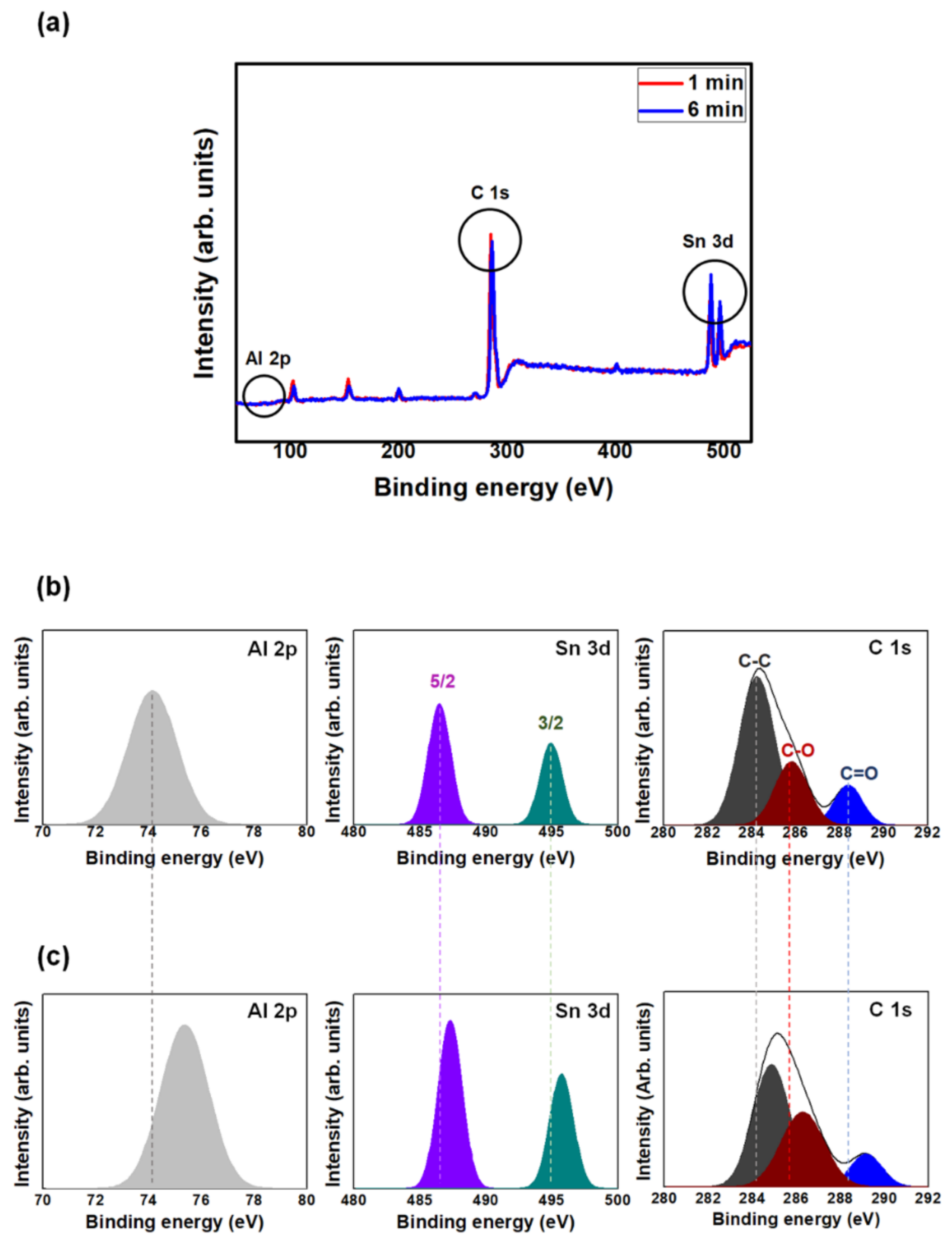
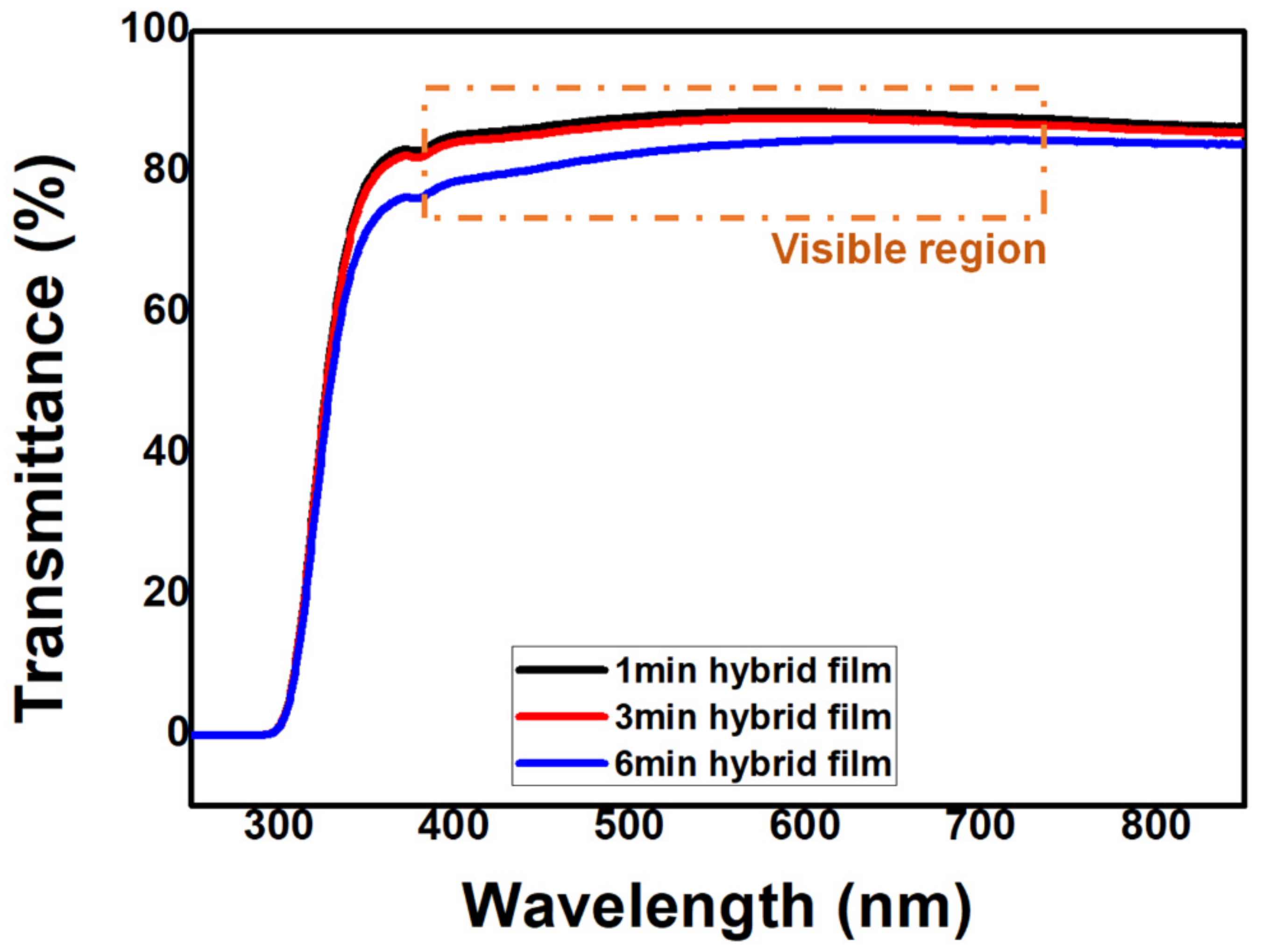
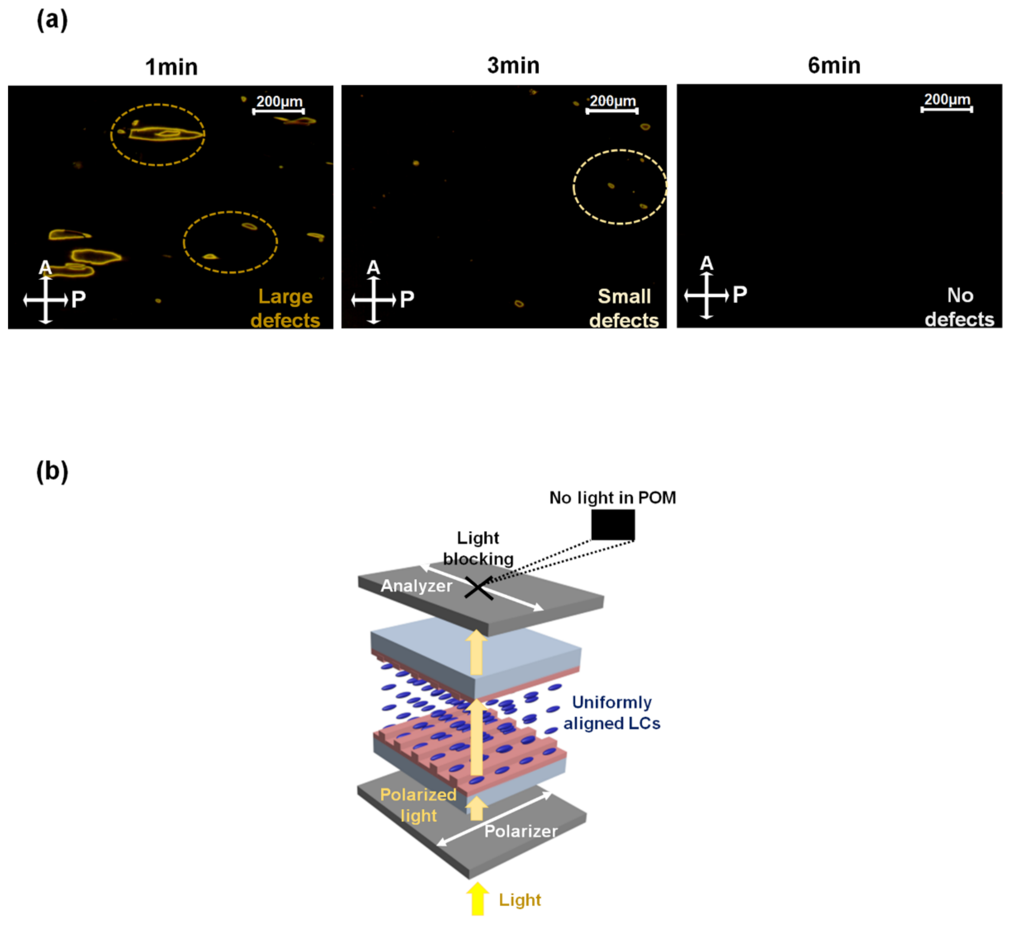
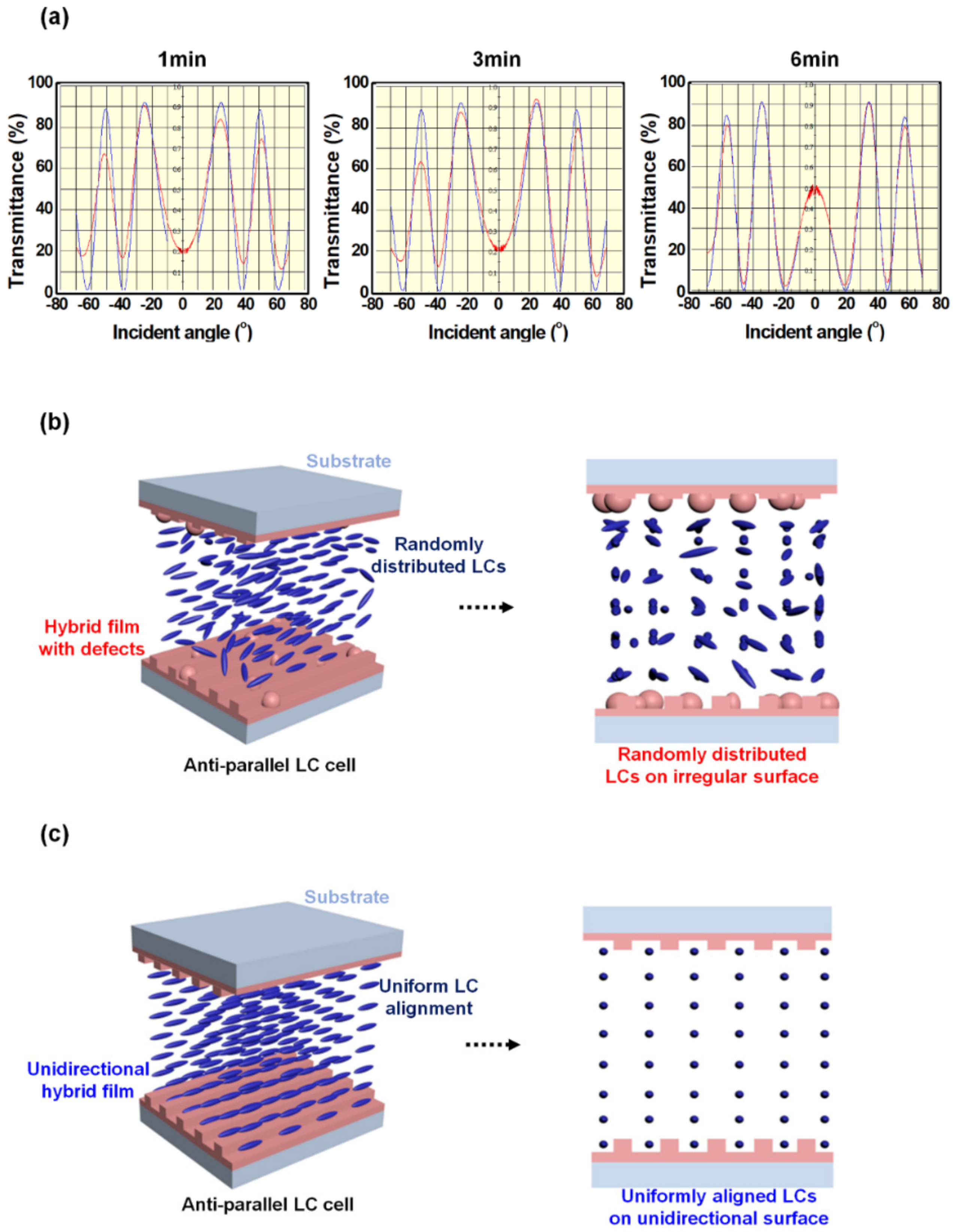
3. Results and Discussion

The surface morphologies of the UV-nanoimprinted hybrid films that were UV-exposed for 1 min, 3 min and 6 min, as well as that of the PDMS master mold, were examined by AFM analysis along with their line profiles, as shown in Figure 3. In the three-dimensional and top-view images, the 1 min (Figure 3b) and 3 min (Figure 3c) UV-exposed UV-curable polymer/AlSnO hybrid films represent some defects, indicating unstable and nonuniform surface state. However, the 6 min (Figure 3d) UV-exposed film exhibits high-resolution uniform nanostructure. It is also seen that the widths and heights of the patterns are similar to those of the PDMS mold (Figure 3a). Therefore, we were assured that the unidirectional nanostructure was shifted from the PDMS mold to the hybrid film via UV-nanoimprint lithography when exposed for 6 min. The shorter UV-exposure time was not enough to construct the unidirectional surface structure. The specific surface nanostructure feature size was analyzed via the AFM line profiles. In the PDMS mold line profile, the periodicity and height of the nanostructure were 820 nm and 30 nm, respectively. In the 1 min and 3 min UV-exposed hybrid films, irregular and nonuniform structures were observed on the surface; thus, the periodicity and height could not be measured. However, the 6 min UV-irradiated film showed regular and uniform structures on the surface, with a periodicity of 760 nm and height of 30 nm. In addition, it could be seen that the surface morphology was derived from the inversed PDMS mold surface morphology. During the UV-NIL process, the spin-coated hybrid solution was covered by PDMS mold, and then the solution was flowed up to the empty spaces of the PDMS mold via capillary force. In that state, curing was progressed, which indicating that the distance between the valleys of PDMS mold structure is converted into the distance between the mountaintops of the hybrid film surface. Because of interface problems such as local variations due to lateral forces during demolding and chemical affinity differences between the PDMS and hybrid material, a slightly reduced periodicity was obtained, but the transferred structure was uniform and well-ordered [41,42]. These results are consistent with those from the AFM image analysis mentioned above. From the above analysis, it is demonstrated that sufficient time is required for UV curing to construct the high-resolution unidirectional nanostructured hybrid film, and the nano-patterns of the PDMS mold are transferred to the UV-curable polymer/AlSnO hybrid film surface well.
To compare and analyze the chemical effects of the hybrid thin film surface according to UV curing time in the UV-NIL process, the chemical composition characteristics of the hybrid films exposed to UV beam for 1 min and 6 min were investigated by XPS analysis. The wide XPS survey scan was conducted in the range of 50–525 eV, as shown in Figure 4a, in which Al 2p, Sn 3d, and C 1s peaks were observed for both films. It indicates the formation of the AlSnO/UV-curable polymer hybrid film via UV-NIL process. For more specific analysis, the 1 min and 6 min UV-exposed film high-resolution Al 2p, Sn 3d, and C 1s spectra were examined, which spectra are the main components of the hybrid film. The results were represented in Figure 4b and Figure 4c, respectively. The Al 2p spectra show one major peak in both hybrid films, and the peaks were centered at 74.15 eV and 75.36 eV, respectively, for 1 min and 6 min UV-exposed films. The positive peak shift with increasing UV exposure time is due to the oxidation effect by the UV curing process. The Sn 3d spectra present two major peaks in both films, indicating Sn 3d 5/2 and Sn 3d 3/2, respectively. These peaks were originated from the spin-orbit splitting. The center binding energies of these peaks are 486.47 eV and 494.92 eV for the 1 min UV-exposed film and 487.29 eV and 495.72 eV for the 6 min UV-exposed film. The Sn 3d spectra were also positively shifted similar to the Al 2p spectra. The hybrid film C 1s spectra present two major peaks, and they were each composed of three sub-peaks. For the 1 min UV-exposed film, these sub-peaks were centered at 284.24, 285.82, and 288.39 eV, corresponding to the C-C, C-O, and C=O bonds, respectively. These peaks were positively shifted to 284.87, 286.28, and 289.17 eV as the UV-exposure time was increased to 6 min, which indicates the oxidation effects of the UV-curing process. The atomic concentrations of the C 1s spectra are listed in Table 1. In the table, the concentration of the main C-C bonding peak decreased remarkably, whereas that of the C-O peak increased with the increase in UV-irradiation time from 1 to 6 min. These results indicate that surface reformation of the hybrid film occurred during the UV-NIL process. The chemically affected (oxidized) hybrid film surface hardened along with transfer of the inverse nanostructure from the PDMS mold. Further, the 6 min UV-exposure time was sufficient to form the high-resolution unidirectional hybrid film nanostructure.
The optical transmittance values of the UV-nanoimprinted hybrid films that were UV-cured for 1 min, 3 min and 6 min were investigated in the range of 250–850 nm to confirm their applicability to LC devices. The resulting graphs are shown in Figure 5. The average transmittance in the visible region (380–740 nm) was measured as 87.51%, 86.56%, and 82.85% for the 1 min, 3 min, and 6 min UV-exposed hybrid films in each. The decrease in transmittance can be attributed to the unidirectional nanostructures that become clearer with increasing UV-exposure time. According to the waveguide mode theory, photons in the visible region are trapped on the periodic nanopatterns on the surface, causing light loss [43]. This results in a decrease in the optical transmittance of the hybrid film. However, considering that the average transmittance values of plain and ITO-coated glasses are 85.44% and 81.82%, respectively, in the visible region and that the corresponding value of the conventionally used polyimide (PI) film is 80–85%, it is confirmed that the unidirectional nanopatterned hybrid film has competitive optical transmittance [12,41]. In addition, the hybrid films show horizontal curves in the visible region without large fluctuations, indicating stable and reliable film states. Therefore, UV-nanoimprinted hybrid films have the potential to be used in advanced LC devices.
To investigate the alignment states of LC molecules on the UV-nanoimprinted hybrid films, AP-LC cells were assembled from the 1 min, 3 min, and 6 min UV-exposed hybrid films. The assembled cells were examined via POM, and the measured POM images are depicted in Figure 6a. The 1 min and 3 min UV-exposed hybrid-film-based LC cells exhibit some defects in the POM images, indicating irregularly distributed LC states. The defects are reduced with the increased UV-irradiation time from 1 min to 3 min. On the contrary, the LC cell based on 6 min UV-irradiated films produces perfect dark images in POM, indicating uniform LC alignment without disclination. The LC cells were located between a vertically crossed polarizer and an analyzer, and the uniformly aligned LCs induces constant light direction which penetrating the LC cells. As a result, perfect light blocking was achieved at the analyzer, and the light could not be detected in the POM image. This process is represented in Figure 6b. With these POM results, it is observed that films with defects in the AFM analysis could not achieve uniform LC alignment on the surface, and films with uniform unidirectional nanostructures observed in the AFM analysis could induce the uniform alignment state of LCs on that surface.
For further analysis on LC alignment state, pretilt angles of the LCs on the UV-nanoimprinted hybrid films were measured in accordance with UV-exposure times. The pretilt angles represent the angles between the LCs and alignment layer. This can be measured from the crystal rotation method which rotating the fabricated LC cell and measuring the light retardation during that rotation [34,35]. In this research, a HeNe laser was used, and the transmittance curves were obtained by rotating the LC cells from −70° to 70° with a latitudinal rotation. The obtained graphs are presented in Figure 7a. In the graphs, the blue curves represent the simulated curves produced from the information on the LCs and fabricated LC cell gaps, whereas the red curves represent the experimental curves obtained from actual measurements. For the 1 min and 3 min UV-exposed hybrid-film-based LC cells, irregular red curves are measured, and high mismatch rates were observed with the blue curves, meaning unstable film states and irregular LC alignment. On the contrary, for the 6 min UV-exposed hybrid-film-based LC cell, a regular experimental curve was observed, which had high concordance rate with the ideal simulation curve, indicating stable film state and reliable pretilt angle data acquisition. These film state analyses are also consistent with the AFM and POM analysis results. The calculated LC pretilt angle on the 6 min UV-exposed hybrid film was 0.04°, which means a homogeneous LC alignment state. When the hybrid film contains defects, such as irregular lumps on the surface, it cannot provide any orientational guidance to the LCs for uniform alignment, which results in randomly distributed LC states, as represented in Figure 7b. On the other hand, a high-resolution uniform unidirectional hybrid film (6 min UV-exposed film) can derive uniform alignment of LCs with anisotropy surface characteristics. The LCs have intrinsically liquid and elastic characteristics, and the elasticity tries to minimize the LC bulk free energy. Therefore, the unidirectional nanopatterns can induce the orientations of the LCs by minimizing distortions and achieving homogeneous and uniform alignment of LCs, as shown in Figure 7c [13]. With these aspects, we confirmed that the unidirectional nanopattern transferred hybrid film could be adopted to high-quality LC systems.

4. Conclusions

We achieved the nanoscaled unidirectional structures of AlSnO and UV-curable polymer hybrid materials via the UV-NIL process, and these films were used to fabricate uniform LC alignment layers. The UV-curing times were controlled to 1 min, 3 min, and 6 min. The AFM data and corresponding line profiles exhibited uniform and well-ordered surface morphologies with a periodicity of 760 nm and height of 30 nm for the 6 min UV-exposed hybrid film surface. The chemical property changes to the hybrid film based on UV exposure time were examined by XPS analysis. The hybrid film exhibited competitive optical transmittance compared to the conventionally used PI layer, implying applicability to LC devices. The LC alignment state was investigated by POM and pretilt angle analysis, and stable, uniform, and homogeneous LC alignment was confirmed. The uniform unidirectional nanopattern on the hybrid film surface induced uniform LC orientations along with surface anisotropic characteristics. Therefore, the proposed UV-NIL process can be adopted to inorganic/organic hybrid materials for unidirectional nanopatterning along with application to high-quality LC systems.

Author Contributions

Conceptualization, D.-W.L.; methodology, J.W.; validation, D.-H.K.; formal analysis, D.-W.L.; investigation, J.-Y.O.; resources, J.W.; writing—original draft preparation, D.-W.L.; visualization, J.-Y.O.; supervision, D.-S.S.; project administration, D.-S.S. All authors have read and agreed to the published version of the manuscript.

Funding

This research received no external funding.

Institutional Review Board Statement

Not applicable.

Informed Consent Statement

Not applicable.

Data Availability Statement

The data presented in this study are available upon request from the corresponding author.

Conflicts of Interest

The authors declare no conflict of interest.

References

  1. Chen, Y.; Xu, D.; Wu, S.-T.; Yamamoto, S.; Haseba, Y.A. A low voltage and submillisecond-response polymer-stabilized blue phase liquid crystal. Appl. Phys. Lett. 2013, 102, 141116. [Google Scholar] [CrossRef] [Green Version]
  2. Song, D.-M.; Jung, K.-H.; Moon, J.-H.; Shin, D.-M. Photochemistry of chalcone and the application of chalcone-derivatives in photo-alignment layer of liquid crystal display. Opt. Mater. 2003, 21, 667–671. [Google Scholar] [CrossRef]
  3. Garbovskiy, Y. Switching between purification and contamination regimes governed by the ionic purity of nanoparticles dispersed in liquid crystals. Appl. Phys. Lett. 2016, 108, 121104. [Google Scholar] [CrossRef]
  4. Nimmy, J.V.; Shiju, E.; Arun, R.; Varma, M.K.R.; Chandrasekharan, K.; Sandhyarani, N.; Varghese, S. Effect of ferroelectric nanoparticles in the alignment layer of twisted nematic liquid crystal display. Opt. Mater. 2017, 67, 7–13. [Google Scholar]
  5. Edwards, D.M.F.; Madden, P.A. A molecular theory of the dielectric permittivity of a nematic liquid crystal. Mol. Phys. 1983, 48, 471–493. [Google Scholar] [CrossRef]
  6. Yan, X.; Mont, F.W.; Poxson, D.J.; Schubert, M.F.; Kim, J.K.; Cho, J.; Schubert, E.F. Refractive-index-matched indium-tin-oxide electrodes for liquid crystal displays. Jpn. J. Appl. Phys. 2009, 48, 120203. [Google Scholar] [CrossRef]
  7. Chen, S.H.; Amer, N.M. Observation of macroscopic collective behavior and new texture in magnetically doped liquid crystals. Phys. Rev. Lett. 1983, 51, 2298–2301. [Google Scholar] [CrossRef] [Green Version]
  8. Kovalchuk, A.I.; Kobzar, Y.L.; Tkachenko, I.M.; Kurioz, Y.I.; Tereshchenko, O.G.; Shekera, O.V.; Nazarenko, V.G.; Shevchenko, V.V. Photoactive fluorinated poly(azomethine)s with azo groups in the main chain for optical storage applications and controlling liquid crystal orientation. ACS Appl. Polym. Mater. 2020, 2, 455–463. [Google Scholar] [CrossRef]
  9. Eguchi, N.; Nimori, S.; Goto, H. Magnetically aligned helical liquid crystal field allows the production of polymer with laser diffraction and prism function. ACS Appl. Polym. Mater. 2020, 2, 5452–5459. [Google Scholar] [CrossRef]
  10. Dolan, J.A.; Cai, H.; Delalande, L.; Li, X.; Martinson, A.B.F.; de Pablo, J.J.; Lopez, D.; Nealey, P.F. Broadband liquid crystal tunable metasurfaces in the visible: Liquid crystal inhomogeneities across the metasurface parameter space. ACS Photonics 2021, 8, 567–575. [Google Scholar] [CrossRef]
  11. Wu, D.; Zhou, J.; Lin, X.; Lin, J.; Shi, L.; Ding, J.; Wu, Q. Structure, luminescence, and energy transfer of a narrow-band green-emitting phosphor Ce5Si3O12N:Tb3+ for near-ultraviolet light-emitting diode-driven liquid-crystal display. ACS Appl. Electron. Mater. 2021, 3, 406–414. [Google Scholar] [CrossRef]
  12. Lee, D.W.; Lee, J.H.; Kim, E.M.; Heo, G.S.; Kim, D.H.; Oh, J.Y.; Liu, Y.; Seo, D.-S. Surface modification of a poly(ethylene-co-vinyl acetate) layer by ion beam irradiation for the uniform alignment of liquid crystals. J. Mol. Liq. 2021, 339, 116700. [Google Scholar] [CrossRef]
  13. Lee, W.-K.; Choi, Y.S.; Kang, Y.-G.; Sung, J.; Seo, D.-S.; Park, C. Super-fast switching of twisted nematic liquid crystals on 2D single wall carbon nanotube networks. Adv. Funct. Mater. 2011, 21, 3843–3850. [Google Scholar] [CrossRef]
  14. Park, H.-G.; Kim, E.-M.; Heo, G.-S.; Jeong, H.-C.; Lee, J.H.; Han, J.-M.; Kim, T.W.; Seo, D.-S. Electro-optical properties of liquid crystal displays based on the transparent zinc oxide films treated by using a rubbing method. Opt. Mater. 2018, 75, 252–257. [Google Scholar] [CrossRef]
  15. Stohr, J.; Samant, M.G.; Luning, J.; Callegari, A.C.; Chaudhari, P.; Doyle, J.P.; Lacey, J.A.; Lien, S.A.; Purushothaman, S.; Speidell, J.L. Liquid crystal alignment on carbonaceous surfaces with orientational order. Science 2001, 292, 2299–2302. [Google Scholar] [CrossRef] [Green Version]
  16. Wu, G.M.; Liu, C.Y.; Sahoo, A.K. RF sputtering deposited a-IGZO films for LCD alignment layer application. Appl. Surf. Sci. 2015, 354, 48–54. [Google Scholar] [CrossRef]
  17. Janning, J.L. Thin film surface orientation for liquid crystals. Appl. Phys. Lett. 1972, 21, 173. [Google Scholar] [CrossRef]
  18. Zhang, L.; Peng, Z.; Yao, L.; Fei, C.; Lv, F.; Xuan, L. Photoalignment of liquid crystals by cinnamate polyelectrolyte layer-by-layer ultrathin film. Appl. Surf. Sci. 2007, 253, 3372–3377. [Google Scholar] [CrossRef]
  19. Chigrinov, V.G.; Kozenkov, V.M.; Kwok, H.S. Photoalignment of Liquid Crystalline Materials; John Wiley & Sons: Chichester, UK, 2008. [Google Scholar]
  20. Gibbons, W.M.; Shannon, P.J.; Sun, S.-T.; Swetlin, B.J. Surface-mediated alignment of nematic liquid crystals with polarized laser light. Nature 1991, 351, 49–50. [Google Scholar] [CrossRef]
  21. Dyadyusha, A.G.; Marusiǐ, T.Y.; Reznikov, Y.A.; Khizhnyak, A.I.; Reshetnyak, V.Y. Orientational effect due to a change in the anisotropy of the interaction between a liquid crystal and a bounding surface. JETP Lett. 1992, 56, 17. [Google Scholar]
  22. Dyadyusha, A.G.; Kozenkov, V.M.; Marusiy, T.Y. Light-induced planar alignment of nematic liquid-crystal by the anisotropic surface without mechanical texture. Ukr. Fiz. Zh. 1991, 36, 1059–1062. [Google Scholar]
  23. Toney, M.F.; Russell, T.P.; Logan, J.A.; Kikuchi, H.; Sands, J.M.; Kumar, S.K. Near-surface alignment of polymers in rubbed films. Nature 1995, 374, 709–711. [Google Scholar] [CrossRef]
  24. Haaren, J.V. Wiping out dirty displays. Nature 2001, 411, 29–30. [Google Scholar] [CrossRef]
  25. Henry, P.S.H. The role of asymmetric rubbing in the generation of static electricity. Br. J. Appl. Phys. 1953, 4, S31. [Google Scholar] [CrossRef]
  26. Jeong, H.-C.; Lee, J.H.; Won, J.; Oh, B.Y.; Kim, D.H.; Lee, D.W.; Song, I.H.; Liu, Y.; Seo, D.-S. One-dimensional surface wrinkling for twisted nematic liquid crystal display based on ultraviolet nanoimprint lithography. Opt. Express 2019, 27, 18094–18101. [Google Scholar] [CrossRef]
  27. Solodar, A.; Cerkauskaite, A.; Drevinskas, R.; Kazansky, P.G.; Abdulhalim, I. Ultrafast laser induced nanostructured ITO for liquid crystal alignment and higher transparency electrodes. Appl. Phys. Lett. 2018, 113, 081603. [Google Scholar] [CrossRef]
  28. Lin, R.; Rogers, J.A. Molecular-scale soft imprint lithography for alignment layers in liquid crystal devices. Nano Lett. 2007, 7, 1613–1621. [Google Scholar] [CrossRef]
  29. Söderström, K.; Escarré, J.; Cubero, O.; Haug, F.-J.; Perregaux, S.; Ballif, C. UV-nano-imprint lithography technique for the replication of back reflectors for n-i-p thin film silicon solar cells. Prog. Photovolt. Res. Appl. 2011, 19, 202–210. [Google Scholar] [CrossRef]
  30. Maury, P.; Turkenburg, D.; Stroeks, N.; Giesen, P.; Barbu, I.; Meinders, E.; van Bremen, A.; Iosad, N.; van der Werf, R.; Onvlee, H. Roll-to-roll UV imprint lithography for flexible electronics. Microelectron. Eng. 2011, 88, 2052–2055. [Google Scholar] [CrossRef]
  31. Won, J.H.; Lee, J.H.; Kim, D.H.; Lee, D.W.; Kim, D.-H.; Jeong, H.-C.; Oh, B.-Y.; Han, J.M.; Seo, D.-S. Electro-optical performance of liquid crystal device based on Al-doped SnO fabricated by sol-gel process. Liq. Cryst. 2020, 47, 345–351. [Google Scholar] [CrossRef]
  32. Argall, F.; Jonscher, A.K. Dielectric properties of thin films of aluminium oxide and silicon oxide. Thin Solid Film. 1968, 2, 185–210. [Google Scholar] [CrossRef]
  33. Yıldırım, M.A.; Yıldırım, S.T.; Sakar, E.F.; Ateşc, A. Synthesis, characterization and dielectric properties of SnO2 thin films. Spectrochim. Acta Part A Mol. Biomol. Spectrosc. 2014, 133, 60–65. [Google Scholar] [CrossRef]
  34. Scheffer, T.J.; Nehring, J. Accurate determination of liquid-crystal tilt bias angles. J. Appl. Phys. 1977, 48, 1783. [Google Scholar] [CrossRef]
  35. Han, K.Y.; Miyashita, T.; Uchida, T. Accurate measurement of the pretilt angle in a liquid crystal cell by an improved crystal rotation method. Mol. Cryst. Liq. Cryst. Sci. Technol. Sect. A Mol. Cryst. Liq. Cryst. 1994, 241, 147–157. [Google Scholar] [CrossRef]
  36. Schier, J.E.S.; Hutchinson, R.A. The influence of hydrogen bonding on radical chain-growth parameters for butyl methacrylate/2-hydroxyethyl acrylate solution copolymerization. Polym. Chem. 2016, 7, 4567–4574. [Google Scholar] [CrossRef] [Green Version]
  37. Li, P.; Chu, Z.; Chen, Y.; Yuan, T.; Yang, Z. One-pot and solvent-free synthesis of castor oil-based polyurethane acrylate oligomers for UV-curable coatings applications. Prog. Org. Coat. 2021, 159, 106398. [Google Scholar] [CrossRef]
  38. Deng, L.; Tang, L.; Qu, J. Synthesis and photopolymerization of novel UV-curable macro-photoinitiators. Prog. Org. Coat. 2020, 141, 105546. [Google Scholar] [CrossRef]
  39. Patacz, C.; Coqueret, X.; Decker, C. Electron-beam initiated polymerization of acrylate compositions 3: Compared reactivity of hexanediol and tripropyleneglycol diacrylates under UV or EB initiation. Radiat. Phys. Chem. 2001, 62, 403–410. [Google Scholar] [CrossRef]
  40. Chang, C.-C.; Hsieh, C.-Y.; Huang, F.-H.; Cheng, L.-P. Preparation of zirconia loaded poly(acrylate) antistatic hard coatings on PMMA substrates. J. Appl. Polym. Sci. 2015, 132, 42411. [Google Scholar] [CrossRef]
  41. Lee, D.W.; Kim, D.H.; Oh, J.Y.; Liu, Y.; Seo, D.-S. Nanopattern transfer on bismuth gallium oxide surface via sol-gel stamp process applied for uniform liquid crystal alignment. Appl. Surf. Sci. 2022, 576, 151712. [Google Scholar] [CrossRef]
  42. Schift, H. Nanoimprint lithography: An old story in modern times? A review. J. Vac. Sci. Technol. B 2008, 26, 458. [Google Scholar] [CrossRef] [Green Version]
  43. Li, X.; Choy, W.C.H.; Huo, L.; Xie, F.; Sha, W.E.I.; Ding, B.; Guo, X.; Li, Y.; Hou, J.; You, J.; et al. Dual plasmonic nanostructures for high performance inverted organic solar cells. Adv. Mater. 2012, 24, 3046–3052. [Google Scholar] [CrossRef] [PubMed]
Figure 1. UV-curable polymers used in this research and their structures of chemical molecules: (a) 2-hydroxyethyl acrylate, (b) tripropylene glycol diacrylate, and (c) dipentaerythritol hexaacrylate.
Crystals 12 00855 g001
Figure 2. Schematic of the unidirectional nanostructure shifting process from PDMS mold to UV-curable polymer/AlSnO hybrid film surface by UV-NIL process.
Crystals 12 00855 g002
Figure 3. (a) PDMS mold and UV-nanoimprinted hybrid films 3-D (left), top-view (middle) AFM images, and corresponding line profiles (right) according to UV exposure time: (b) 1 min, (c) 3 min, and (d) 6 min.
Crystals 12 00855 g003
Figure 4. (a) XPS survey-scan spectra in the range of 50 to 525 eV for the 1 min and 6 min UV-exposed hybrid films. High resolution Al 2p, Sn 3d, and C 1s core-level XPS data for the (b) 1 min and (c) 6 min UV-exposed hybrid films.
Crystals 12 00855 g004
Figure 5. Optical transmittance graphs of the UV-curable polymer/AlSnO hybrid films according to UV-irradiation time for the wavelength range of 250–850 nm.
Crystals 12 00855 g005
Figure 6. (a) POM images of the fabricated AP-LC cells assembled from 1 min, 3 min, and 6 min UV-exposed hybrid films (the directions of the analyzer (A) and polarizer (P) are presented by white arrows). (b) Schematic of the light path during passage through the AP-LC cell comprising uniformly aligned LCs on unidirectional hybrid films; no light leakage is observed.
Crystals 12 00855 g006
Figure 7. (a) Oscillated transmittance graphs as functions of the incidence angle (from –70° to 70°) of the AP–LC cells produced from 1 min, 3 min, and 6 min UV–exposed hybrid films. (b) Irregular (with defects) and (c) uniform unidirectional surface hybrid–film-based AP–LC cells with their LC alignment state and corresponding front view.
Crystals 12 00855 g007
Table 1. Atomic concentrations of variously bound carbons on the surface of the 1 min and 6 min UV-exposed hybrid films.
UV Exposure TimeC-C (At%)C-O (At%)C=O (At%)
1 min61.7224.9113.37
6 min51.1936.9211.89
Publisher’s Note: MDPI stays neutral with regard to jurisdictional claims in published maps and institutional affiliations.

