
Fabrication and Investigation of Spectral Properties of a Dielectric Slab Waveguide Photonic Crystal Based Fano-Filter


 ,
,  ,
,  and
and 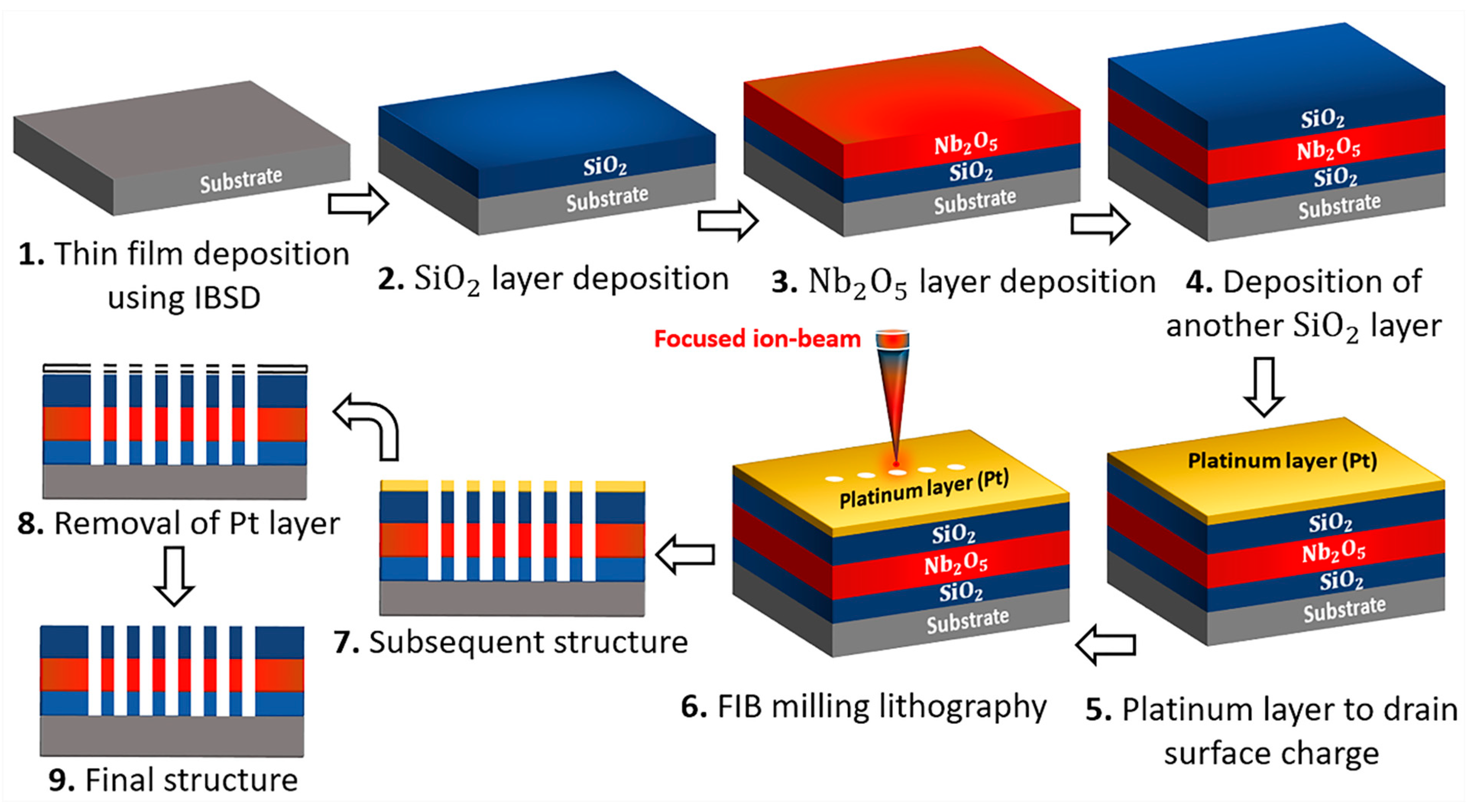
Abstract
:1. Introduction
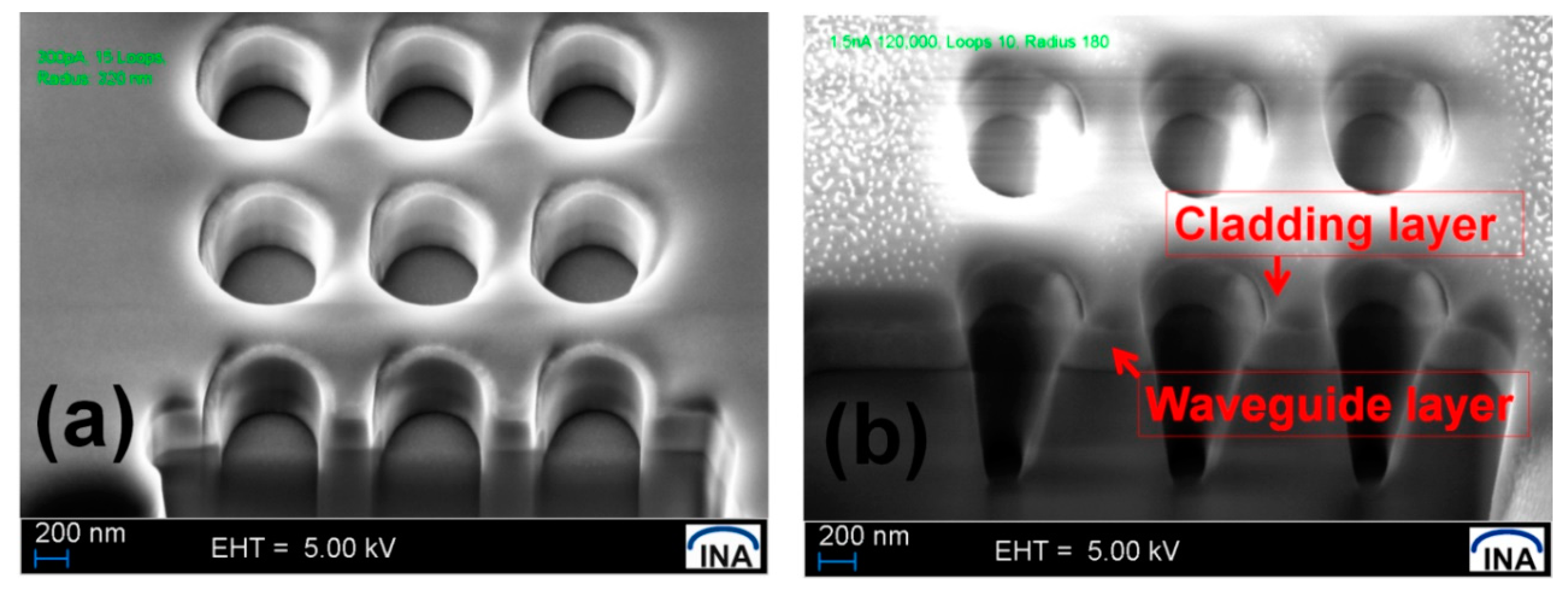
2. Materials and Methods
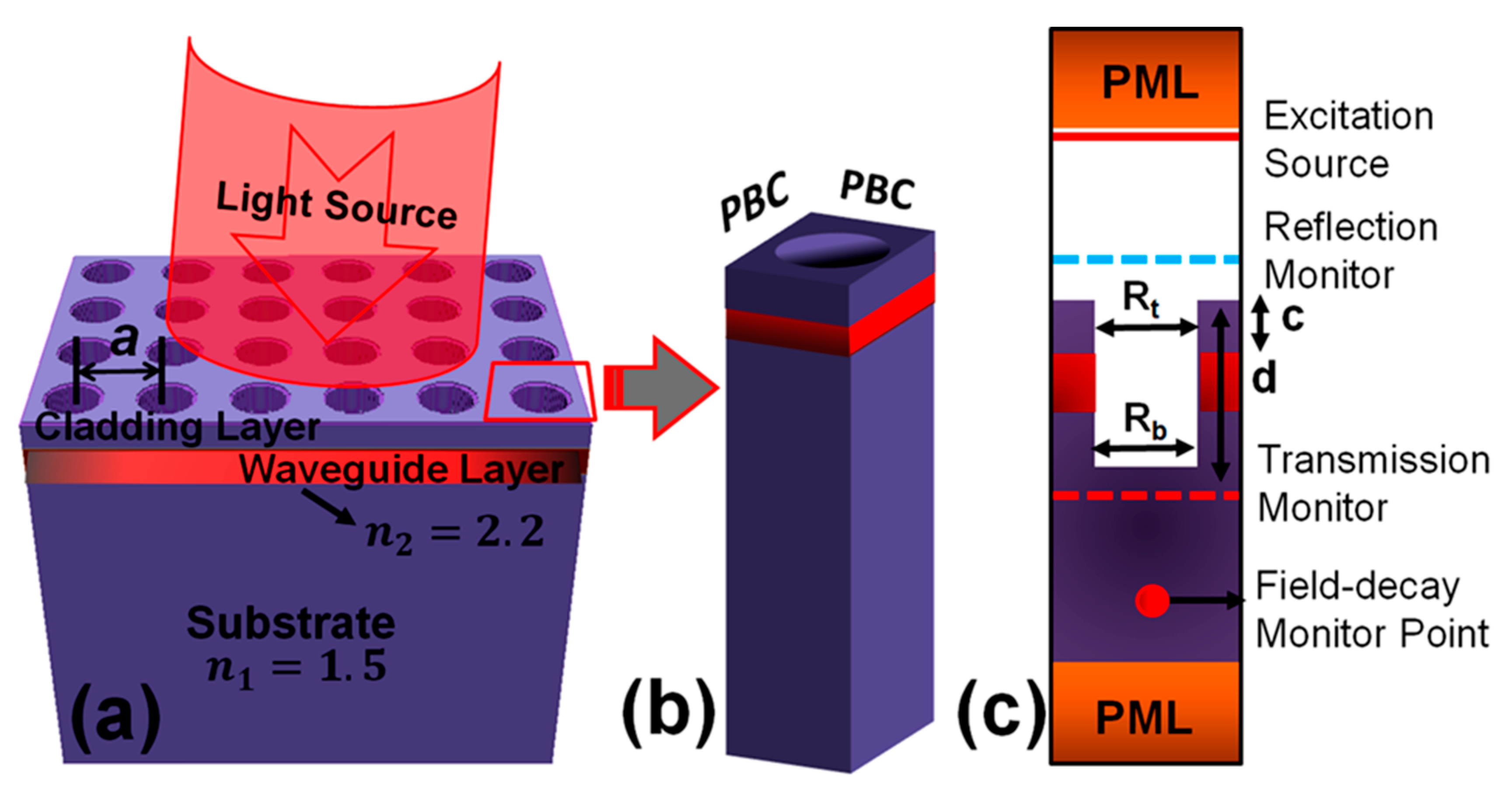
3. Simulation Model
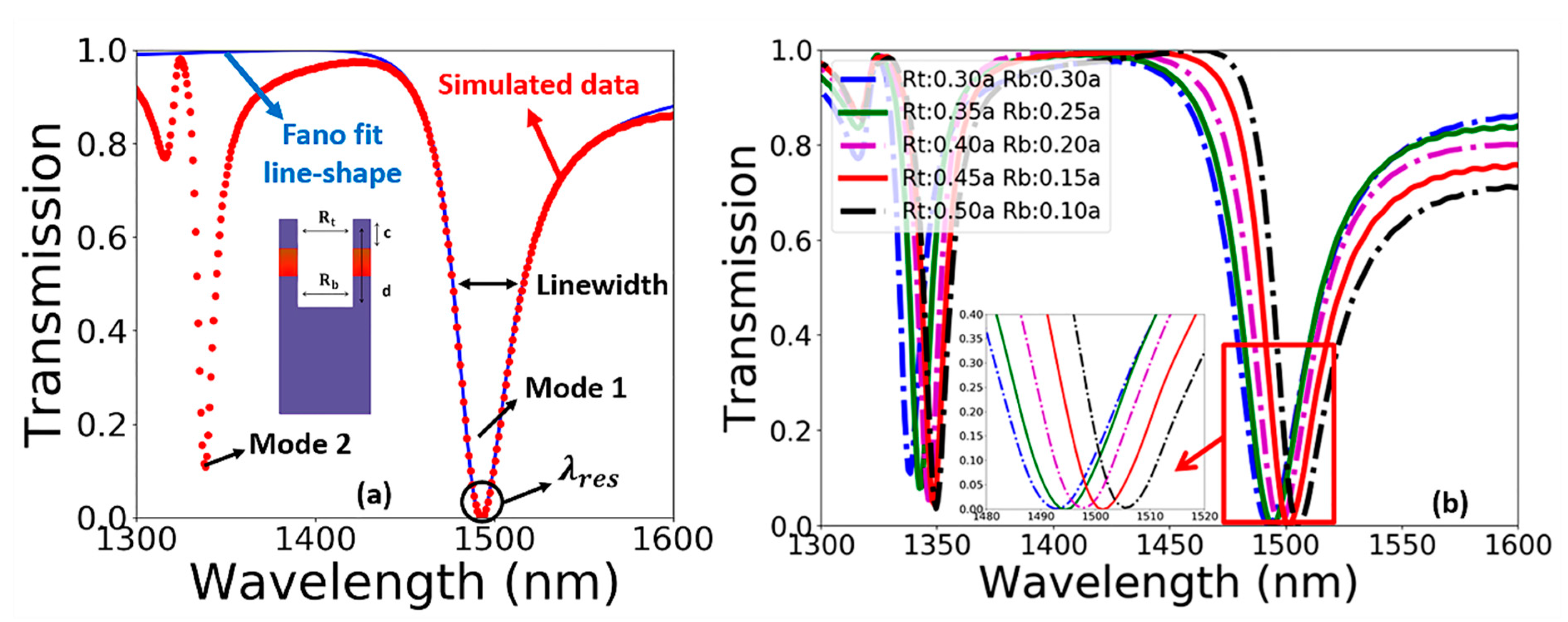
4. Spectral Characteristics of Fano-Filters
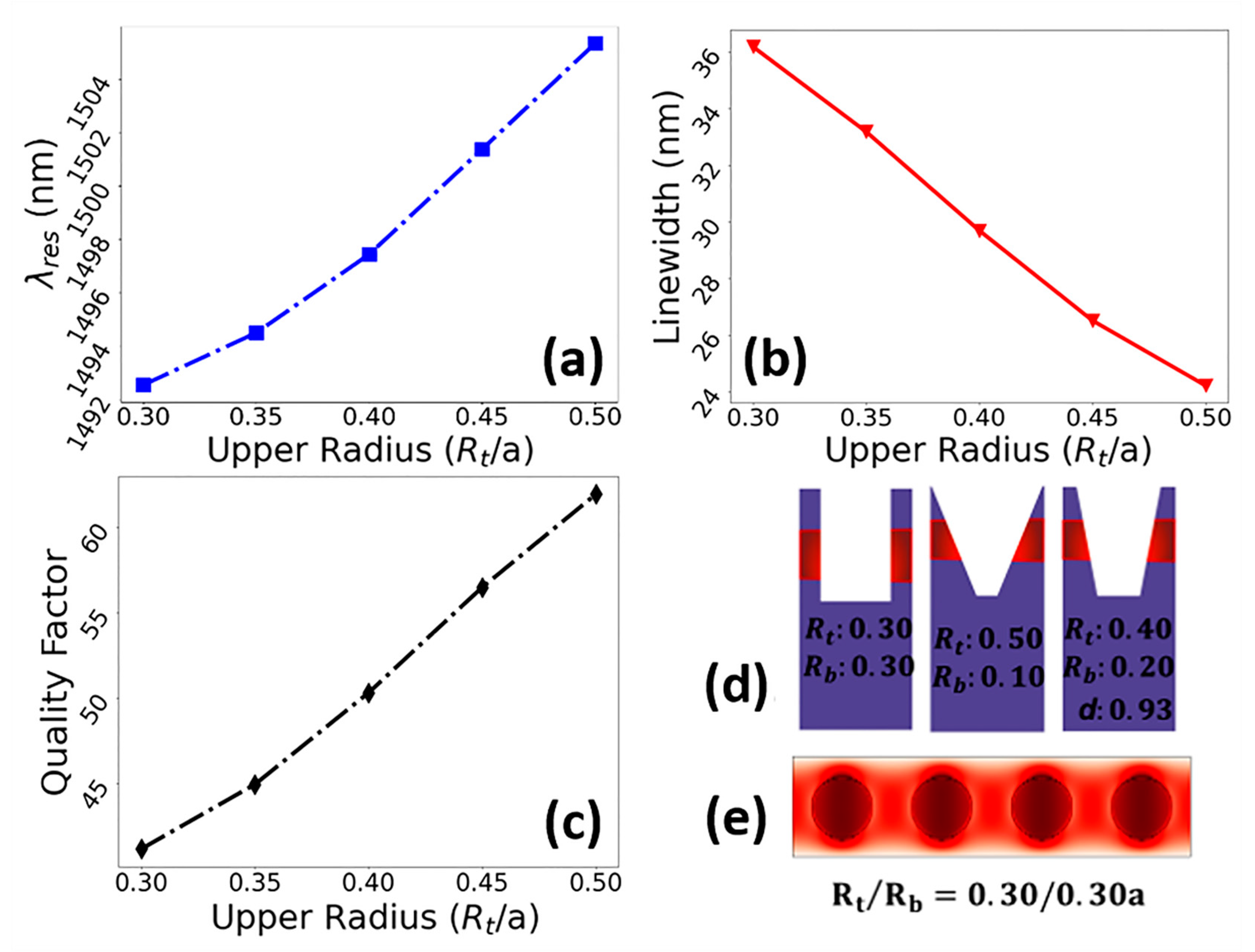
4.1. PhC Element Shape-Dependent Resonances
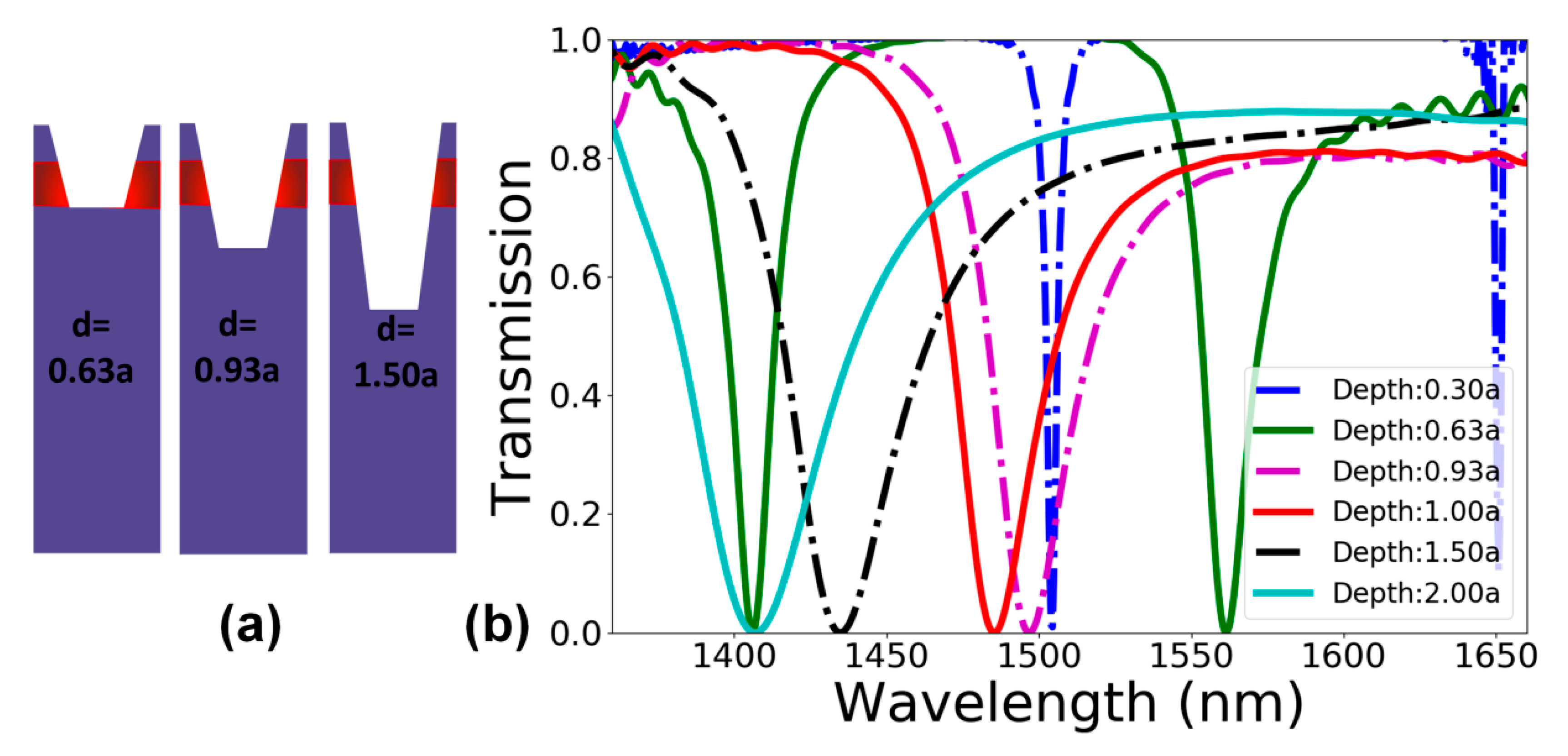
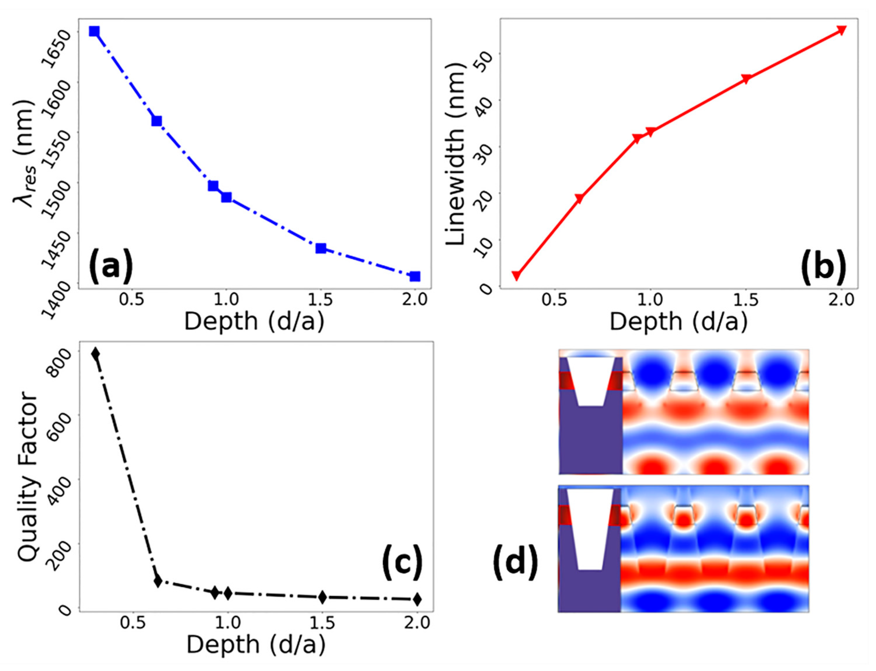
4.2. PhC Element Depth Dependence of Resonances
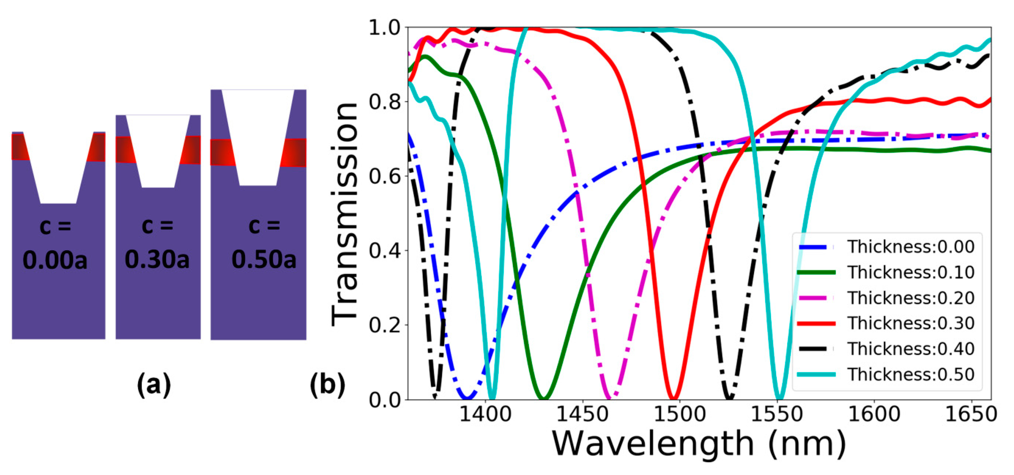
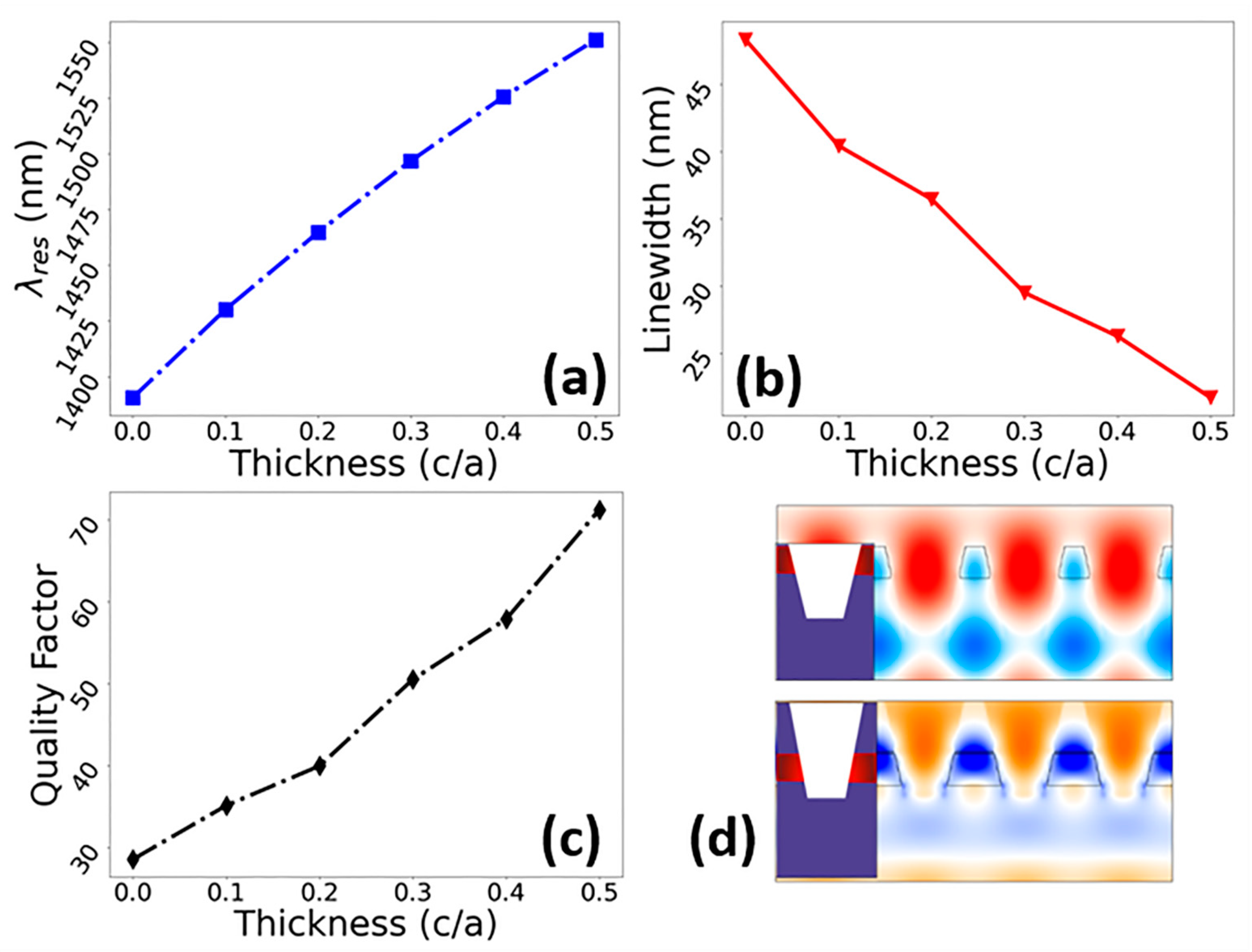
4.3. Cladding-Layer Thickness Dependence of Resonances
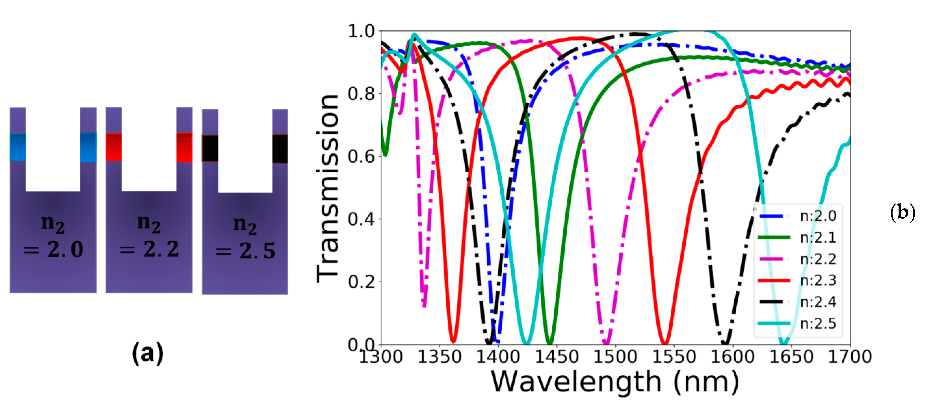
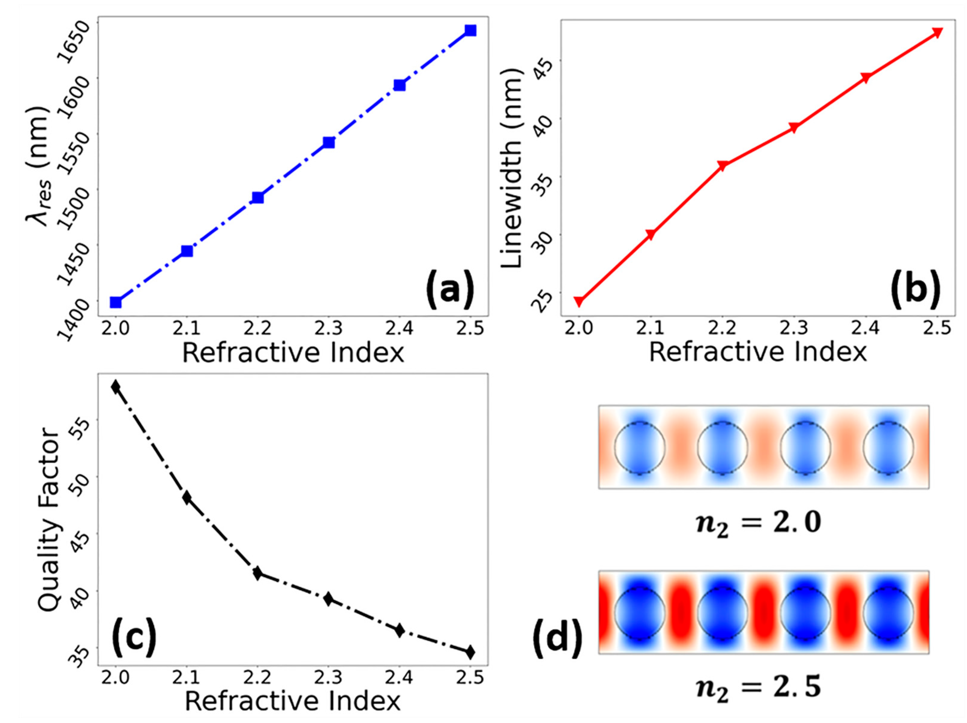
4.4. Refractive Index Dependence of Resonances
5. Conclusions
Author Contributions
Funding
Acknowledgments
Conflicts of Interest
References
- John, S. Strong Localization of Photons in Certain Disordered Superlattices. Phys. Rev. Lett. 1987, 58, 2486. [Google Scholar] [CrossRef] [PubMed] [Green Version]
- Yablonovitch, E. Inhibited Spontaneous Emission in Solid-State Physics and Electronics. Phys. Rev. Lett. 1987, 581–584. [Google Scholar] [CrossRef] [PubMed] [Green Version]
- Magnusson, R.; Wang, S.S. New Principle for Optical Filters. Appl. Phys. Lett. 1992, 61, 1022–1024. [Google Scholar] [CrossRef]
- Butt, M.A.; Khonina, S.N.; Kazanskiy, N.L. Recent Advances in Photonic Crystal Optical Devices: A Review. Opt. Laser Technol. 2021, 142, 107265. [Google Scholar] [CrossRef]
- Fatemeh, G.; Entezar, S.R.; Razi, S. Graphene Based Photonic Crystal Optical Filter: Design and Exploration of the Tunability. Phys. Lett. A 2019, 383, 2551–2560. [Google Scholar]
- Vlasov, Y.A.; O’boyle, M.; Hamann, H.F.; McNab, S.J. Active control of slow light on a chip with photonic crystal waveguides. Nature 2005, 438, 65–69. [Google Scholar] [CrossRef]
- Wang, Q.; Xiao, M.; Liu, H.; Zhu, S.; Chan, C.T. Measurement of the Zak phase of photonic bands through the interface states of a metasurface/photonic crystal. Phys. Rev. B 2016, 93, 041415. [Google Scholar] [CrossRef] [Green Version]
- Chen, F. A Tunable High-Efficiency Optical Switch Based on Graphene Coupled Photonic Crystals Structure. J. Mod. Opt. 2017, 64, 1531–1537. [Google Scholar] [CrossRef]
- Fariborz, P.; Malmir, M.R. Reconfigurable All Optical Half Adder and Optical XOR and AND Logic Gates Based on 2D Photonic Crystals. Opt. Quantum Electron. 2020, 52, 1–8. [Google Scholar]
- Baker, J.E.; Sriram, R.; Miller, B.L. Two-dimensional photonic crystals for sensitive microscale chemical and biochemical sensing. Lab Chip 2015, 15, 971–990. [Google Scholar] [CrossRef] [Green Version]
- Butt, M.A.; Khonina, S.N.; Kazanskiy, N.L. 2D-Photonic Crystal Heterostructures for the Realization of Compact Photonic Devices. Photonics Nanostruct.-Fundam. Appl. 2021, 44, 100903. [Google Scholar] [CrossRef]
- Hadzialic, S.; Kim, S.; Sudbø, A.S.N.; Solgaard, O. Two-Dimensional Photonic Crystals Fabricated in Monolithic Single-Crystal Silicon. IEEE Photonics Technol. Lett. 2010, 22, 67–69. [Google Scholar] [CrossRef]
- Khan, Y. Design and Numerical Simulation of Dielectric Photonic Crystal Devices and Investigation of an Optical Characterization Method. Ph.D. Thesis, University of Kassel, Kassel, Germany, 2017. [Google Scholar]
- Chen, A.; Chua, S.-J.; Fonstad, C.G., Jr.; Wang, B.; Wilhelmi, O. Two-Dimensional Photonic Crystals Fabricated by Nanoimprint Lithography. Available online: https://www.researchgate.net/profile/Benzhong-Wang/publication/289980749_Patterning_of_two-dimensional_photonic_crystal_structures_by_nanoimprint_lithography/links/5695fb3708ae3ad8e33d98a4/Patterning-of-two-dimensional-photonic-crystal-structures-by-nanoimprint-lithography.pdf (accessed on 16 December 2021).
- Huang, H.W.; Lin, C.H.; Huang, J.K.; Lee, K.Y.; Lin, C.F.; Yu, C.C.; Tsai, J.Y.; Hsueh, R.; Kuo, H.C.; Wang, S.C. Investigation of GaN-based Light Emitting Diodes with Nano-Hole Patterned Sapphire Substrate (NHPSS) by Nano-Imprint Lithography. Mater. Sci. Eng. B 2009, 164, 76–79. [Google Scholar] [CrossRef]
- Götte, N.; Kusserow, T.; Winkler, T.; Sarpe, C.; Englert, L.; Otto, D.; Meinl, T.; Khan, Y.; Zielinski, B.; Senftleben, A.; et al. Temporally Shaped Femtosecond Laser Pulses for Creation of functional Sub-100 nm Structures in Dielectrics. In Optically Induced Nanostructures; König, K., Ostendorf, A., Eds.; de Gruyter: Berlin, Germany, 2015; pp. 47–72. [Google Scholar]
- Rybin, M.V.; Khanikaev, A.B.; Inoue, M.; Samusev, K.B.; Steel, M.J.; Yushin, G.; Limonov, M.F. Fano resonance between Mie and Bragg scattering in photonic crystals. Phys. Rev. Lett. 2009, 103, 023901. [Google Scholar] [CrossRef] [PubMed] [Green Version]
- Fan, S.; Joannopoulos, J.D. Analysis of Guided Resonances in Photonic Crystal Slabs. Phys. Rev. B 2002, 65, 235112. [Google Scholar] [CrossRef] [Green Version]
- Fan, S.; Suh, W.; Joannopoulos, J.D. Temporal coupled-mode theory for the Fano resonance in optical resonators. J. Opt. Soc. Am. A 2003, 20, 569–572. [Google Scholar] [CrossRef] [PubMed] [Green Version]
- Limonov, M.F.; Rybin, M.V.; Poddubny, A.N.; Kivshar, Y.S. Fano Resonances in Photonics. Nat. Photonics 2017, 11, 543–554. [Google Scholar] [CrossRef]
- Galli, M.; Portalupi, S.L.; Belotti, M.; Andreani, L.C.; O’Faolain, L.; Krauss, T.F. Light scattering and Fano resonances in high-Q photonic crystal nanocavities. Appl. Phys. Lett. 2009, 94, 071101. [Google Scholar] [CrossRef] [Green Version]
- Sturmberg, B.C.; Dossou, K.B.; Botten, L.C.; McPhedran, R.C.; De Sterke, C.M. Fano resonances of dielectric gratings: Symmetries a broadband filtering. Opt. Express 2015, 23, A1672–A1686. [Google Scholar] [CrossRef]
- Shuai, Y.; Zhao, D.; Singh Chadha, A.; Seo, J.H.; Yang, H.; Fan, S.; Ma, Z.; Zhou, W. Coupled double-layer Fano resonance photonic crystal filters with lattice-displacement. Appl. Phys. Lett. 2013, 103, 241106. [Google Scholar] [CrossRef]
- Cao, G.; Dong, S.; Zhou, L.M.; Zhang, Q.; Deng, Y.; Wang, C.; Zhang, H.; Chen, Y.; Qiu, C.W.; Liu, X. Fano resonance in artificial photonic molecules. Adv. Opt. Mater. 2020, 8, 1902153. [Google Scholar] [CrossRef]
- Nguyen, V.A.; Ngo, Q.M.; Le, K.Q. Efficient color filters based on Fano-like guided-mode resonances in photonic crystal slabs. IEEE Photonics J. 2018, 10, 1–8. [Google Scholar] [CrossRef]
- Caselli, N.; Intonti, F.; La China, F.; Riboli, F.; Gerardino, A.; Bao, W.; Bargioni, A.W.; Li, L.; Linfield, E.H.; Pagliano, F.; et al. Ultra-subwavelength phase-sensitive Fano-imaging of localized photonic modes. Light Sci. Appl. 2015, 4, e326. [Google Scholar] [CrossRef] [Green Version]
- Shuai, Y.; Zhao, D.; Tian, Z.; Seo, J.H.; Plant, D.V.; Ma, Z.; Fan, S.; Zhou, W. Double-layer Fano resonance photonic crystal filters. Opt. Express 2013, 21, 24582–24589. [Google Scholar] [CrossRef] [Green Version]
- Hossain, M.N.; Justice, J.; Lovera, P.; McCarthy, B.; O’Riordan, A.; Corbett, B. High aspect ratio nano-fabrication of photonic crystal structures on glass wafers using chrome as hard mask. Nanotechnology 2014, 25, 355301. [Google Scholar] [CrossRef] [PubMed]
- Joshi-Imre, A.; Bauerdick, S. Direct-Write Ion Beam Lithography. J. Nanotechnol. 2014, 2014, 170415. [Google Scholar] [CrossRef] [Green Version]
- Steve, R.; Robert, P. A Review of Focused Ion Beam Applications in Microsystem Technology. J. Micromech. Microeng. 2001, 11, 287–300. [Google Scholar]
- Lonergan, A.; Breda, M.; O’Dwyer, C. Metallo-Dielectric Photonic Crystals and Bandgap Blue-Shift. arXiv 2021, arXiv:2105.06280. [Google Scholar]
- Prather, D.W.; Shi, S.; Sharkawy, A.; Murakowski, J.; Schneider, G.J. Photonic Crystals, Theory, Applications and Fabrications; Wiley: Hoboken, NJ, USA, 2009. [Google Scholar]
- Ullah, A.; Wilke, H.; Memon, I.; Shen, Y.; Nguyen, D.T.; Woidt, C.; Hillmer, H. Stress relaxation in dual ion beam sputtered Nb2O5 and SiO2 thin films: Application in a Fabry–Pérot filter array with 3D nanoimprinted cavities. J. Micromech. Microeng. 2015, 25, 055019. [Google Scholar] [CrossRef]
- Lambert, E.; Fiers, M.; Nizamov, S.; Tassaert, M.; Johnson, S.G.; Bienstman, P.; Bogaerts, W. Python Bindings for the Open-Source Electromagnetic Simulator Meep. Comput. Sci. Eng. 2010, 13, 53–65. [Google Scholar] [CrossRef] [Green Version]
- Oskooi, A.F.; Roundy, D.; Ibanescu, M.; Bermel, P.; Joannopoulos, J.D.; Johnson, S.G. Meep: A Flexible Free-Software Package for Electromagnetic Simulations by the FDTD Method. Comput. Phys. Commun. 2010, 181, 687–702. [Google Scholar] [CrossRef]


Publisher’s Note: MDPI stays neutral with regard to jurisdictional claims in published maps and institutional affiliations. |
© 2022 by the authors. Licensee MDPI, Basel, Switzerland. This article is an open access article distributed under the terms and conditions of the Creative Commons Attribution (CC BY) license (https://creativecommons.org/licenses/by/4.0/).
Share and Cite
Khan, Y.; Rehman, A.U.; Batool, B.A.; Noor, M.; Butt, M.A.; Kazanskiy, N.L.; Khonina, S.N. Fabrication and Investigation of Spectral Properties of a Dielectric Slab Waveguide Photonic Crystal Based Fano-Filter. Crystals 2022, 12, 226. https://doi.org/10.3390/cryst12020226
Khan Y, Rehman AU, Batool BA, Noor M, Butt MA, Kazanskiy NL, Khonina SN. Fabrication and Investigation of Spectral Properties of a Dielectric Slab Waveguide Photonic Crystal Based Fano-Filter. Crystals. 2022; 12(2):226. https://doi.org/10.3390/cryst12020226
Chicago/Turabian StyleKhan, Yousuf, Atiq Ur Rehman, Bibi A. Batool, Mahain Noor, Muhammad A. Butt, Nikolay L. Kazanskiy, and Svetlana N. Khonina. 2022. "Fabrication and Investigation of Spectral Properties of a Dielectric Slab Waveguide Photonic Crystal Based Fano-Filter" Crystals 12, no. 2: 226. https://doi.org/10.3390/cryst12020226