


Effect of Growth Temperature on Crystallization of Ge1−xSnx Films by Magnetron Sputtering
Abstract
:1. Introduction
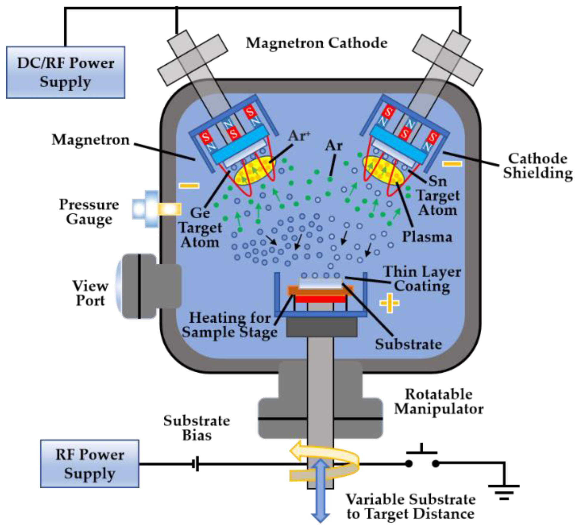
2. Materials and Methods
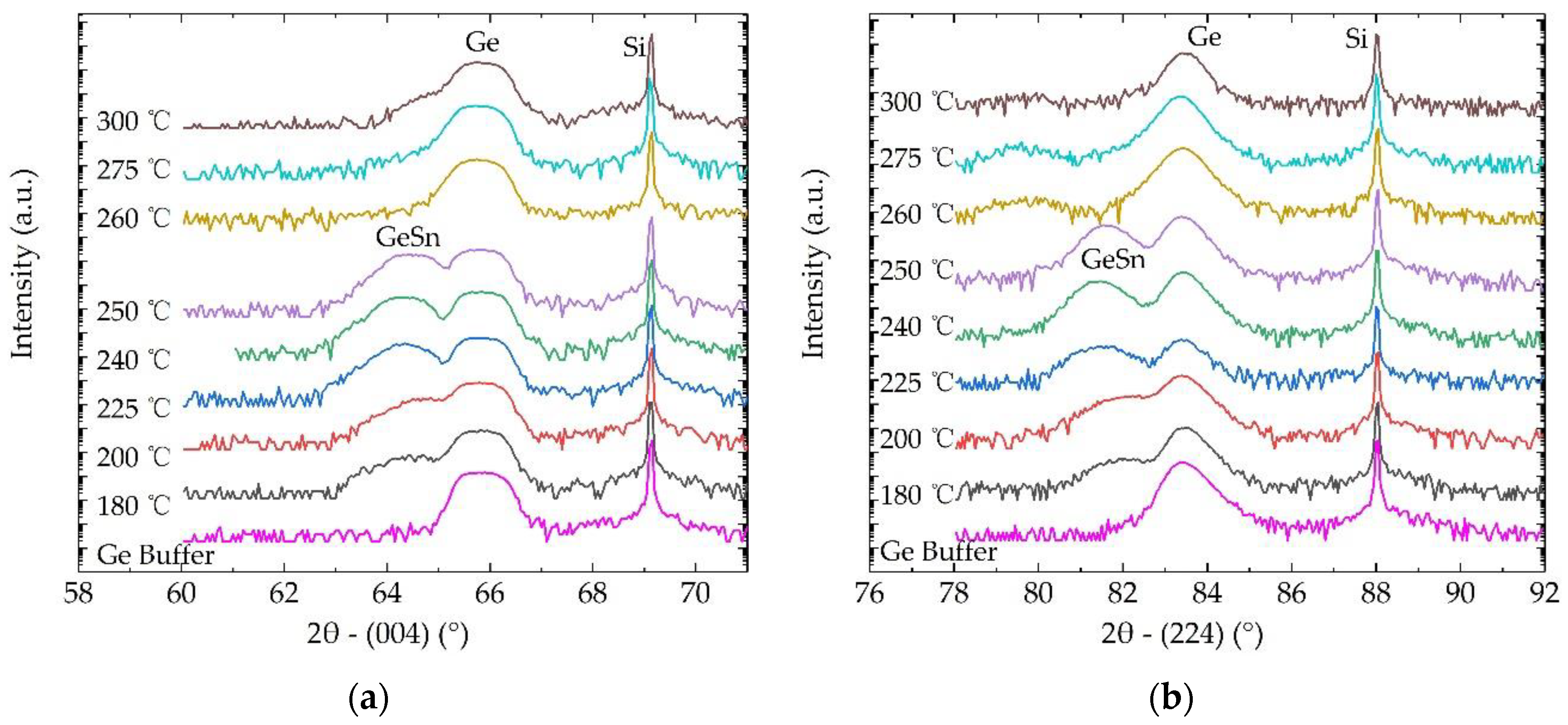
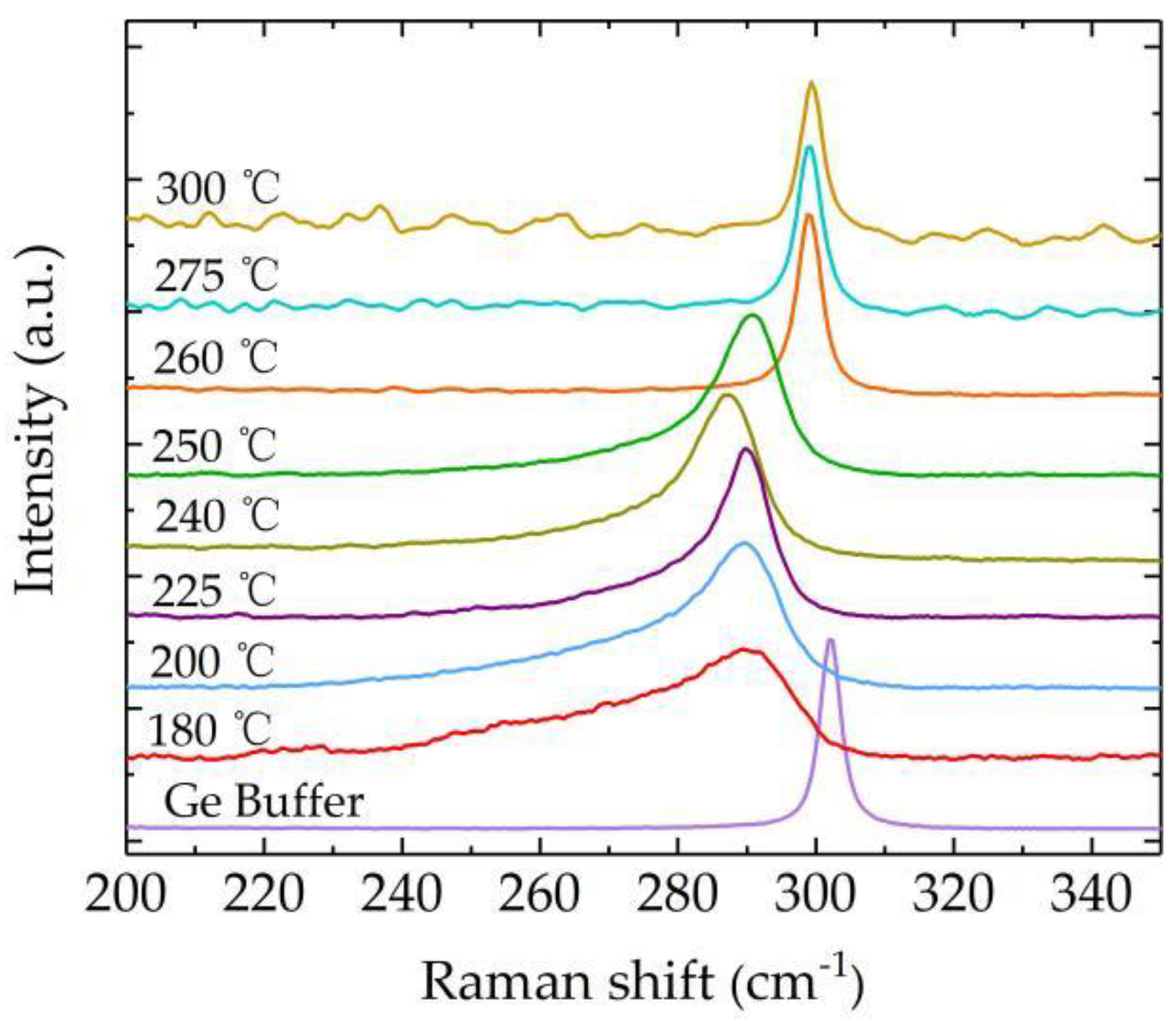
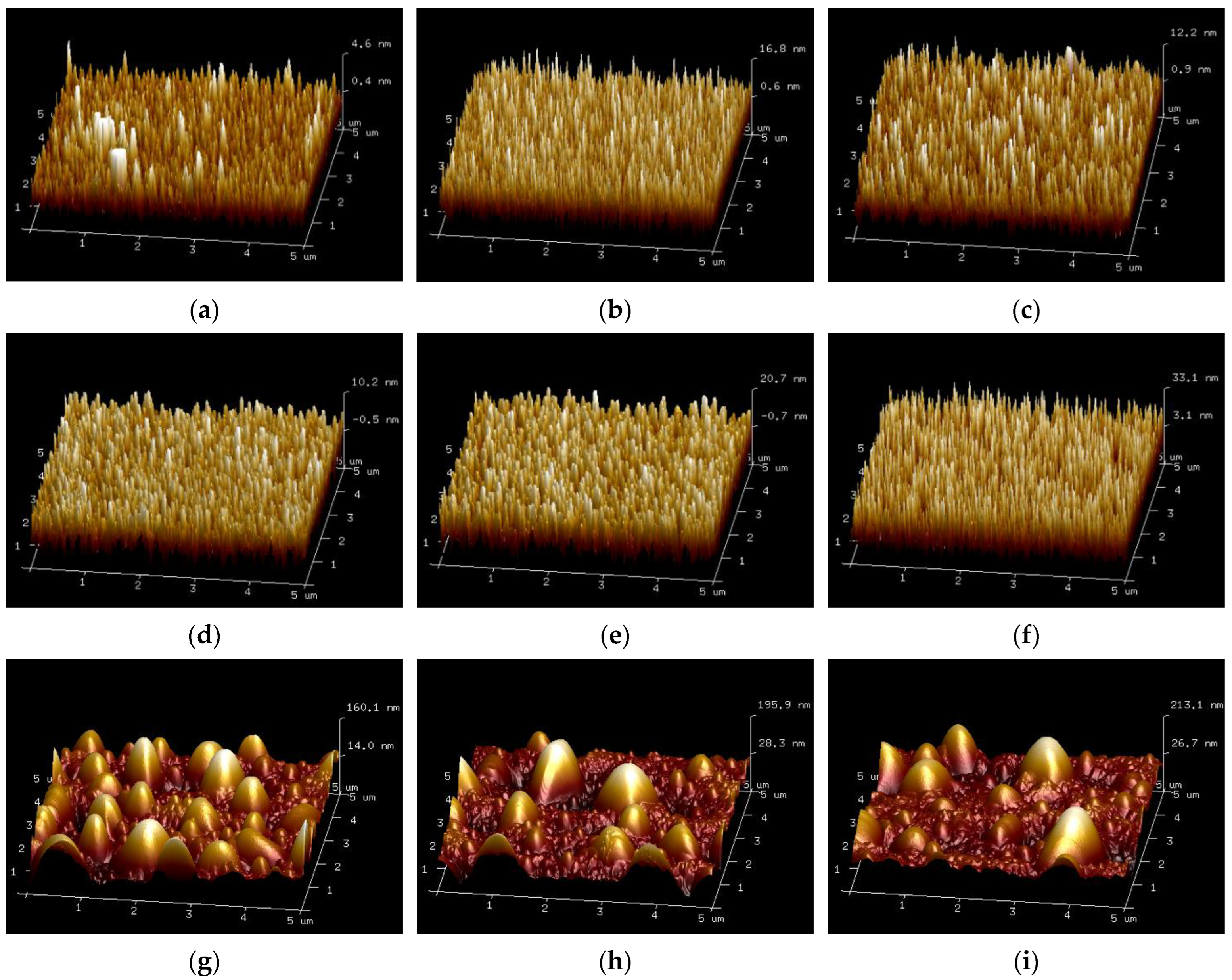
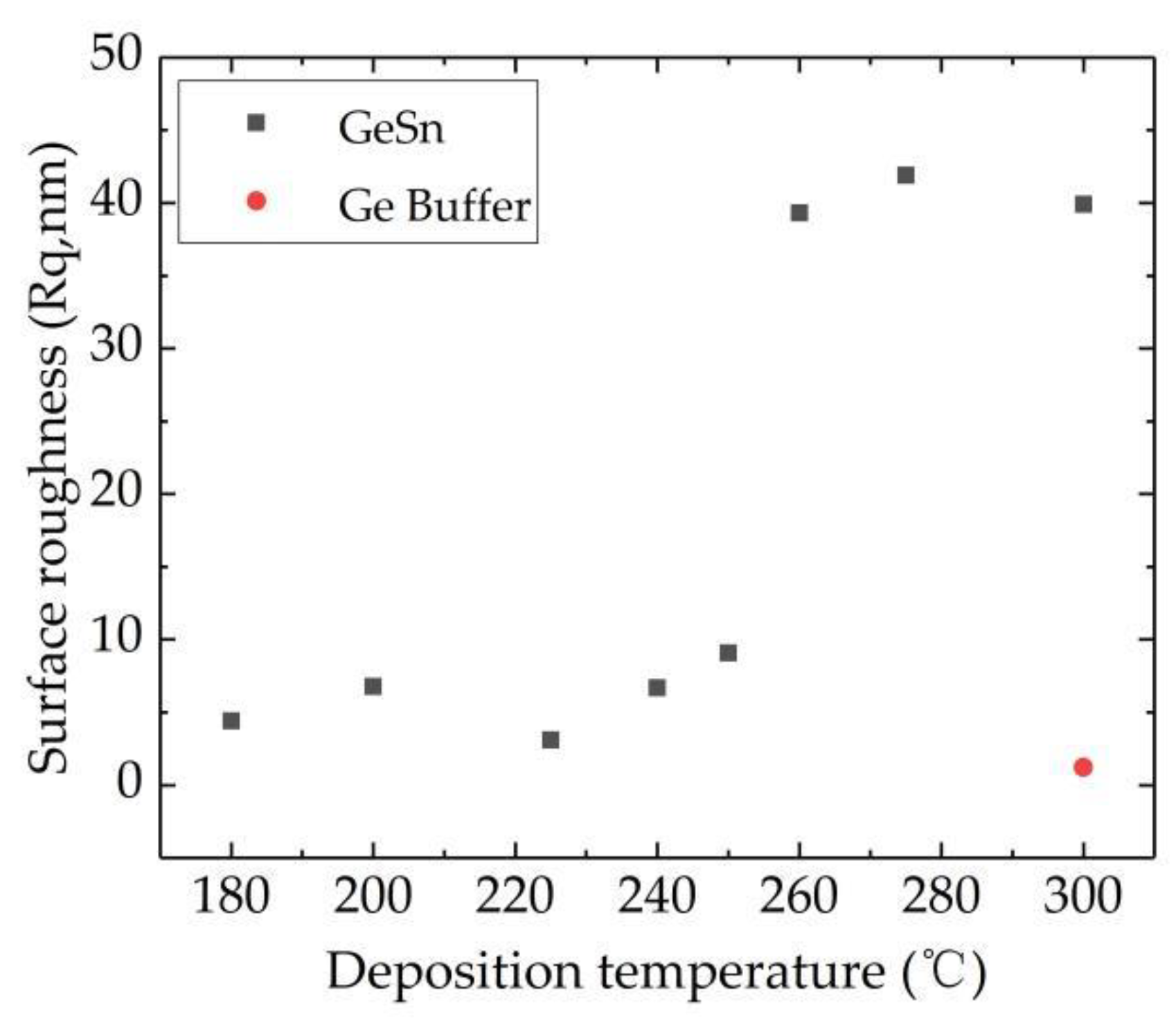
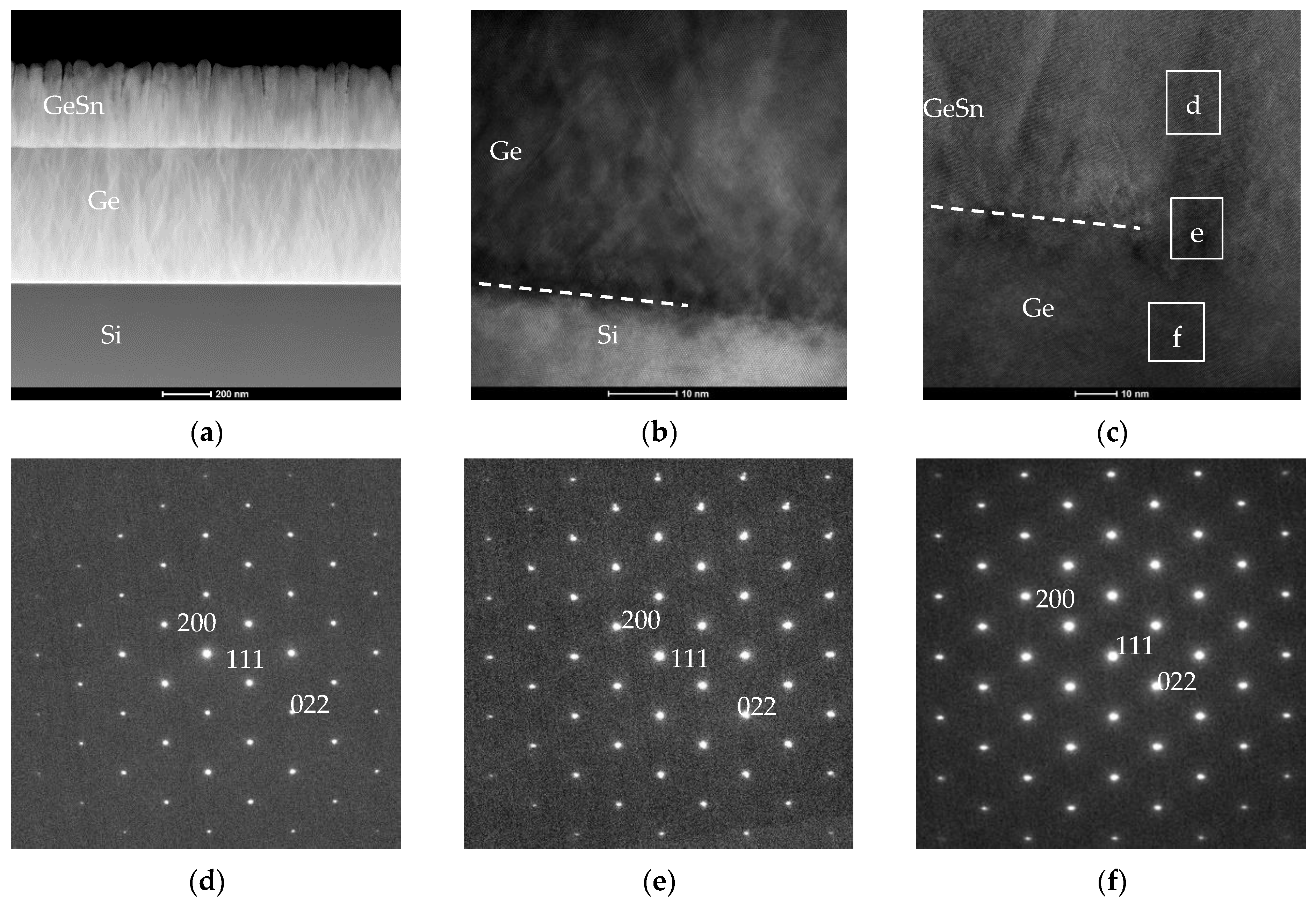
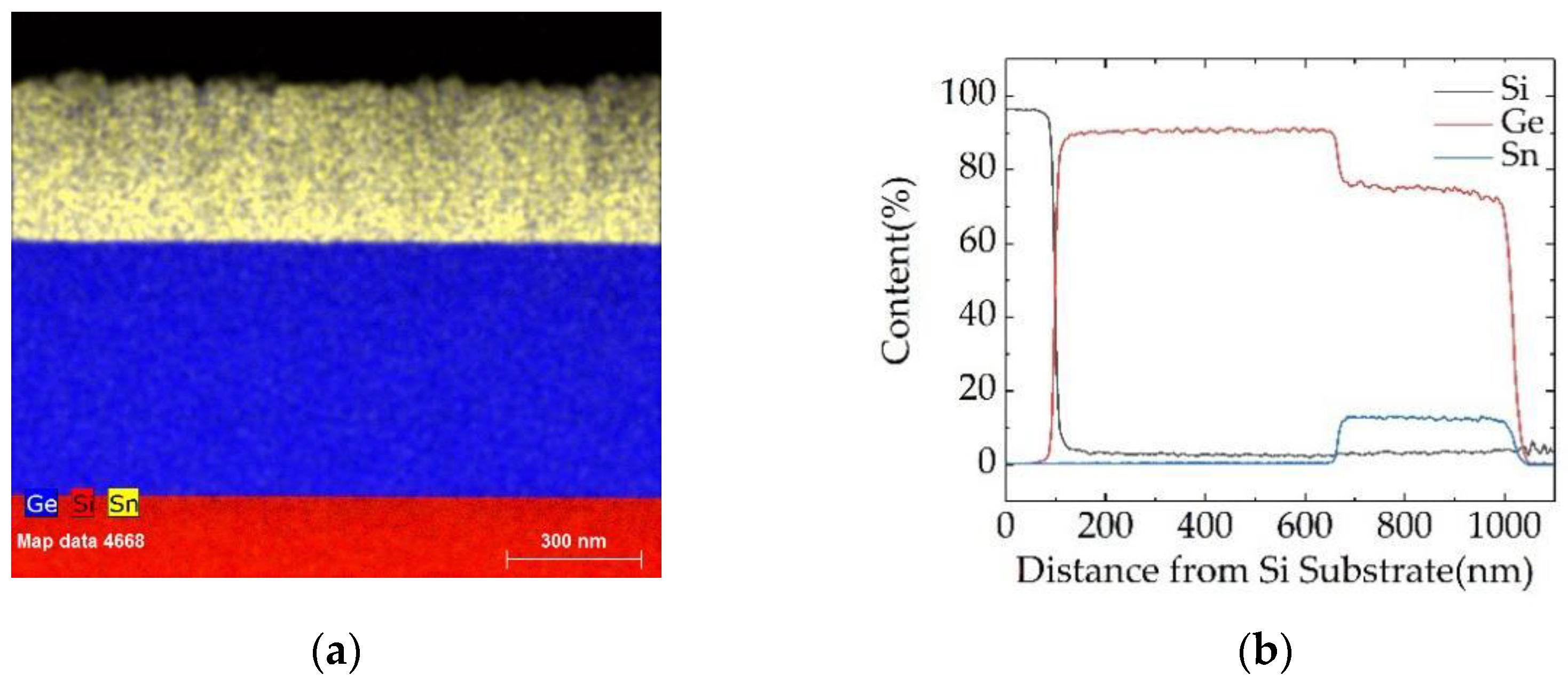
3. Results and Discussion
4. Conclusions
Author Contributions
Funding
Data Availability Statement
Acknowledgments
Conflicts of Interest
References
- Tsai, C.H.; Lin, K.C.; Cheng, C.Y.; Lee, K.C.; Cheng, H.H.; Chang, G.E. GeSn lateral p-i-n waveguide photodetectors for mid-infrared integrated photonics. Opt. Lett. 2021, 46, 864–867. [Google Scholar] [CrossRef] [PubMed]
- Buzynin, Y.N.; Shengurov, V.G.; Denisov, S.A.; Yunin, P.A.; Chalkov, V.Y.; Drozdov, M.N.; Korolyov, S.A.; Nezhdanov, A.V. High Hole Mobility of Polycrystalline GeSn Layers Grown by Hot-Wire Chemical Vapor Deposition on Diamond Substrates. Phys. Status Solidi-Rapid Res. Lett. 2022, 16, 2100421. [Google Scholar] [CrossRef]
- Moto, K.; Yoshimine, R.; Suemasu, T.; Toko, K. Improving carrier mobility of polycrystalline Ge by Sn doping. Sci. Rep. 2018, 8, 14832. [Google Scholar] [CrossRef] [PubMed] [Green Version]
- Sau, J.D.; Cohen, M.L. Possibility of increased mobility in Ge-Sn alloy system. Phys. Rev. B 2007, 75, 045208. [Google Scholar] [CrossRef]
- Anas, E.; Dan, B.; Nils, V.D.D.; Konstantinos, P.; Gilles, P.; Nicolas, Z.; Etienne, H.; Xavier, C.; Sébastien, S.; Isabelle, S.; et al. Ultra-low-threshold continuous-wave and pulsed lasing in tensile-strained GeSn alloys. Nat. Photonics 2020, 14, 375–382. [Google Scholar]
- Uchida, N.; Hattori, J.; Lieten, R.R.; Ohishi, Y.; Takase, R.; Ishimaru, M.; Fukuda, K.; Maeda, T.; Locquet, J.P. Carrier and heat transport properties of poly-crystalline GeSn films for thin-film transistor applications. J. Appl. Phys. 2019, 126, 145105. [Google Scholar] [CrossRef]
- Zhang, L.; Hong, H.Y.; Yu, C.Y.; Li, C.; Chen, S.Y.; Huang, W.; Wang, J.Y.; Wang, H. Poly-GeSn Junctionless Thin-Film Transistors on Insulators Fabricated at Low Temperatures via Pulsed Laser Annealing. Phys. Status Solidi-Rapid Res. Lett. 2019, 13, 1900420. [Google Scholar] [CrossRef]
- Moto, K.; Yamamoto, K.; Imajo, T.; Suemasu, T.; Nakashima, H.; Toko, K. Sn Concentration Effects on Polycrystalline GeSn Thin Film Transistors. IEEE Electron Device Lett. 2021, 42, 1735–1738. [Google Scholar] [CrossRef]
- Mizoguchi, T.; Ishiyama, T.; Moto, K.; Imajo, T.; Suemasu, T.; Toko, K. Solid-Phase Crystallization of GeSn Thin Films on GeO2-Coated Glass. Phys. Status Solidi-Rapid Res. Lett. 2022, 16, 2100509. [Google Scholar] [CrossRef]
- Zhu, X.M.; Cui, M.; Wang, Y.; Yu, T.J.; Li, Q.Y.; Deng, J.X.; Gao, H.L. Evaluation of electricity generation on GeSn single-junction solar cell. Int. J. Energy Res. 2022, 1–8. [Google Scholar] [CrossRef]
- Wu, S.T.; Xu, S.Q.; Zhou, H.; Jin, Y.H.; Chen, Q.M.; Huang, Y.C.; Zhang, L.; Gong, X.; Tan, C.S. High-Performance Back-Illuminated Ge0.92Sn0.08/Ge Multiple-Quantum-Well Photodetector on Si Platform for SWIR Detection. IEEE J. Sel. Top. Quantum Electron. 2022, 28, 1–9. [Google Scholar] [CrossRef]
- Wang, N.; Xue, C.L.; Wan, F.S.; Zhao, Y.; Xu, G.Y.; Liu, Z.; Zheng, J.; Zuo, Y.H.; Cheng, B.W.; Wang, Q.M. High-Performance GeSn Photodetector Covering All Telecommunication Bands. IEEE Photonics J. 2021, 13, 1–9. [Google Scholar] [CrossRef]
- Tran, H.; Pham, T.; Margetis, J.; Zhou, Y.Y.; Dou, W.; Grant, P.C.; Grant, J.M.; Al-Kabi, S.; Sun, G.; Soref, R.A.; et al. Si-Based GeSn Photodetectors toward Mid-Infrared Imaging Applications. ACS Photonics 2019, 6, 2807–2815. [Google Scholar] [CrossRef] [Green Version]
- Zhang, L.F.; Shu, B.; Jiang, R.H.; Gao, Y.L.; Zhang, H.M.; Xuan, R.X.; Hu, H.Y. Short wave infrared LEDs based on strained GeSn. Micro Opt. Tech Lett. 2018, 60, 1151–1154. [Google Scholar] [CrossRef]
- Oehme, M.; Werner, J.; Gollhofer, M.; Schmid, M.; Kaschel, M.; Kasper, E.; Schulze, J. Room-Temperature Electroluminescence from GeSn Light-Emitting Pin Diodes on Si. IEEE Photonics Technol. Lett. 2011, 23, 1751–1753. [Google Scholar] [CrossRef]
- Zhou, Y.Y.; Dou, W.; Du, W.; Pham, T.; Ghetmiri, S.A.; Al-Kabi, S.; Mosleh, A.; Alher, M.; Margetis, J.; Tolle, J.; et al. Systematic study of GeSn heterostructure-based light-emitting diodes towards mid-infrared applications. J. Appl. Phys. 2016, 120, 023102. [Google Scholar] [CrossRef]
- Chang, C.; Li, H.; Huang, S.H.; Lin, L.C.; Cheng, H.H. Temperature-dependent electroluminescence from GeSn heterojunction light-emitting diode on Si substrate. Jpn. J. Appl. Phys. 2016, 55, 04EH03. [Google Scholar] [CrossRef]
- Kim, Y.; Assali, S.; Burt, D.; Jung, Y.; Joo, H.J.; Chen, M.; Ikonic, Z.; Moutanabbir, O.; Nam, D. Enhanced GeSn Microdisk Lasers Directly Released on Si. Adv. Opt. Mater. 2022, 10, 2101213. [Google Scholar] [CrossRef]
- Margetis, J.; Al-Kabi, S.; Du, W.; Dou, W.; Zhou, Y.Y.; Pham, T.; Grant, P.; Ghetmiri, S.; Mosleh, A.; Li, B.H.; et al. Si-Based GeSn Lasers with Wavelength Coverage of 2–3 μm and Operating Temperatures up to 180 K. ACS Photonics 2018, 5, 827–833. [Google Scholar] [CrossRef]
- Chang, G.-E.; Yu, S.-Q.; Liu, J.F.; Cheng, H.-H.; Soref, R.A.; Sun, G. Achievable Performance of Uncooled Homojunction GeSn Mid-Infrared Photodetectors. IEEE J. Sel. Top. Quantum Electron. 2022, 28, 1–11. [Google Scholar] [CrossRef]
- Kumar, H.; Basu, R. Effect of Defects on the Performance of Si-Based GeSn/Ge Mid-Infrared Phototransistors. IEEE Sens. J. 2021, 21, 5975–5982. [Google Scholar] [CrossRef]
- Zhou, Y.Y.; Ojo, S.; Wu, C.W.; Miao, Y.H.; Tran, H.; Grant, J.M.; Abernathy, G.; Amoah, S.; Bass, J.; Salamo, G.; et al. Electrically injected GeSn lasers with peak wavelength up to 2.7 μm. Photonics Res. 2022, 10, 222–229. [Google Scholar] [CrossRef]
- Asano, T.; Shimura, Y.; Nakatsuka, O.; Zaima, S. Influence of Sn incorporation and growth temperature on crystallinity of Ge1−xSnx layers heteroepitaxially grown on Ge(110) substrates. Thin Solid Film. 2013, 531, 504–508. [Google Scholar] [CrossRef]
- Chen, R.; Huang, Y.C.; Gupta, S.; Lin, A.C.; Sanchez, E.; Kim, Y.; Saraswat, K.C.; Kamins, T.I.; Harris, J.S. Material characterization of high Sn-content, compressively-strained GeSn epitaxial films after rapid thermal processing. J. Cryst. Growth 2013, 365, 29–34. [Google Scholar] [CrossRef]
- Trumbore, F.A. Solid Solubilities and Electrical Properties of Tin in Germanium Single Crystals. J. Electrochem. Soc. 1956, 103, 597–600. [Google Scholar] [CrossRef]
- Zheng, J.; Li, L.; Zhou, T.; Zuo, Y.; Li, C.; Cheng, B.; Wang, Q. Growth of Crystalline Ge1−xSnx Films on Si (100) by Magnetron Sputtering. ECS Solid State Lett. 2014, 3, 111–113. [Google Scholar] [CrossRef]
- Rathore, J.; Nanwani, A.; Mukherjee, S.; Das, S.; Moutanabbir, O.; Mahapatra, S. Composition uniformity and large degree of strain relaxation in MBE-grown thick GeSn epitaxial layers, containing 16% Sn. J. Phys. D Appl. Phys. 2021, 54, 185105. [Google Scholar] [CrossRef]
- Wei, L.; Miao, Y.; Pan, R.; Zhang, W.W.; Li, C.; Lu, H.; Chen, Y.F. Highly strained Ge1−xSnx alloy films with high Sn compositions grown by MBE. J. Cryst. Growth 2021, 557, 125996. [Google Scholar] [CrossRef]
- Wan, F.S.; Xu, C.; Wang, X.Y.; Xu, G.Y.; Cheng, B.W.; Xue, C.L. Study of strain evolution mechanism in Ge1_xSnx materials grown by low temperature molecular beam epitaxy. J. Cryst. Growth 2022, 577, 126399. [Google Scholar] [CrossRef]
- Olorunsola, O.; Said, A.; Ojo, S.; Abernathy, G.; Saha, S.; Wangila, E.; Grant, J.; Stanchu, H.; Acharya, S.; Du, W.; et al. Enhanced carrier collection efficiency of GeSn single quantum well towards all-group-IV photonics applications. J. Phys. D Appl. Phys. 2022, 55, 305101. [Google Scholar] [CrossRef]
- Kong, Z.Z.; Wang, G.L.; Liang, R.R.; Su, J.L.; Xun, M.; Miao, Y.H.; Gu, S.H.; Li, J.J.; Cao, K.H.; Lin, H.X.; et al. Growth and Strain Modulation of GeSn Alloys for Photonic and Electronic Applications. Nanomaterials 2022, 12, 981. [Google Scholar] [CrossRef] [PubMed]
- Grant, J.; Abernathy, G.; Olorunsola, O.; Ojo, S.; Amoah, S.; Wanglia, E.; Saha, S.K.; Sabbar, A.; Du, W.; Alher, M.; et al. Growth of Pseudomorphic GeSn at Low Pressure with Sn Composition of 16.7%. Materials 2021, 14, 7637. [Google Scholar] [CrossRef] [PubMed]
- Tsukamoto, T.; Hirose, N.; Kasamatsu, A.; Matsui, T.; Suda, Y. Effects of Low-Temperature GeSn Buffer Layers on Sn Surface Segregation During GeSn Epitaxial Growth. Electron. Mater. Lett. 2020, 16, 9–13. [Google Scholar] [CrossRef]
- Khelidj, H.; Portavoce, A.; Bertoglio, M.; Descoins, M.; Patout, L.; Hoummada, K.; Hallén, A.; Charaï, A.; Benoudia, M.C.; Mangelinck, D. Ge(Sn) growth on Si(001) by magnetron sputtering. Mater. Today Commun. 2021, 26, 101915. [Google Scholar] [CrossRef]
- Liu, X.Q.; Zheng, J.; Li, M.M.; Wan, F.S.; Niu, C.Q.; Liu, Z.; Zuo, Y.H.; Xue, C.L.; Cheng, B.W. Growth of relaxed GeSn film with high Sn content via Sn component-grade buffer layer structure. J. Phys. D Appl. Phys. 2021, 54, 435101. [Google Scholar] [CrossRef]
- Abdi, S.; Assali, S.; Atalla, M.R.M.; Koelling, S.; Warrender, J.M.; Moutanabbir, O. Recrystallization and interdiffusion processes in laser-annealed strain-relaxed metastable Ge0.89Sn0.11. J. Appl. Phys. 2022, 131, 105304. [Google Scholar] [CrossRef]
- Oka, H.; Mizubayashi, W.; Ishikawa, Y.; Uchida, N.; Mori, T.; Endo, K. Non-equilibrium solid-phase growth of amorphous GeSn layer on Ge-on-insulator wafer induced by flash lamp annealing. Appl. Phys. Express 2021, 14, 025505. [Google Scholar] [CrossRef]
- Cai, H.J.; Qian, K.; An, Y.Y.; Lin, G.Y.; Wu, S.S.; Ding, H.K.; Huang, W.; Chen, S.Y.; Wang, J.Y.; Li, C. Thickness-dependent behavior of strain relaxation and Sn segregation of GeSn epilayer during rapid thermal annealing. J. Alloys Compd. 2022, 904, 164068. [Google Scholar] [CrossRef]
- Wang, W.; Zhou, Q.; Dong, Y.; Tok, E.S.; Yeo, Y.-C. Critical thickness for strain relaxation of Ge1−xSnx (x ≤ 0.17) grown by molecular beam epitaxy on Ge(001). Appl. Phys. Lett. 2015, 106, 232106. [Google Scholar] [CrossRef]
- Lin, K.C.; Huang, P.R.; Li, H.; Cheng, H.H.; Chang, G.E. Temperature-dependent characteristics of GeSn/Ge multiple-quantum-well photoconductors on silicon. Opt. Lett. 2021, 46, 3604–3607. [Google Scholar] [CrossRef]
- Assali, S.; Nicolas, J.; Moutanabbir, O. Enhanced Sn incorporation in GeSn epitaxial semiconductors via strain relaxation. J. Appl. Phys. 2019, 125, 025304. [Google Scholar] [CrossRef]
- Dou, W.; Benamara, M.; Mosleh, A.; Margetis, J.; Grant, P.; Zhou, Y.Y.; Al-Kabi, S.; Du, W.; Tolle, J.; Li, B.H.; et al. Investigation of GeSn Strain Relaxation and Spontaneous Composition Gradient for Low-Defect and High-Sn Alloy Growth. Sci. Rep. 2018, 8, 5640. [Google Scholar] [CrossRef] [PubMed] [Green Version]
- Joe, M.; Yu, S.-Q.; Nupur, B.; Li, B.H.; Du, W.; John, T. Strain engineering in epitaxial Ge1−xSnx: A path towards low-defect and high Sn-content layers. Semicond. Sci. Technol. 2017, 32, 124006. [Google Scholar]
- Zheng, J.; Liu, Z.; Zhang, Y.W.; Zuo, Y.H.; Li, C.B.; Xue, C.L.; Cheng, B.W.; Wang, Q.M. Growth of high-Sn content (28%) GeSn alloy films by sputtering epitaxy. J. Cryst. Growth 2018, 492, 29–34. [Google Scholar] [CrossRef]
- Dev, S.; Khiangte, K.R.; Lodha, S. Wafer-scale mono-crystalline GeSn alloy on Ge by sputtering and solid phase epitaxy. J. Phys. D-Appl. Phys. 2020, 53, 21LT01. [Google Scholar] [CrossRef]
- Qian, L.; Tong, J.C.; Suo, F.; Liu, L.; Fan, W.J.; Luo, Y.; Zhang, D.H. GeSn/GaAs Hetero-Structure by Magnetron Sputtering. IEEE J. Quantum Electron. 2020, 56, 1–5. [Google Scholar] [CrossRef]
- Abdel-Rahman, M.; Alduraibi, M.; Hezam, M.; Ilahi, B. Sputter deposited GeSn alloy: A candidate material for temperature sensing layers in uncooled microbolometers. Infrared Phys. Technol. 2019, 97, 376–380. [Google Scholar] [CrossRef]
- Zhang, L.; Wang, Y.S.; Chen, N.L.; Lin, G.Y.; Li, C.; Huang, W.; Chen, S.Y.; Xu, J.F.; Wang, J.Y. Raman scattering study of amorphous GeSn films and their crystallization on Si substrates. J. Non-Cryst. Solids 2016, 448, 74–78. [Google Scholar] [CrossRef]
- Tsukamoto, T.; Hirose, N.; Kasamatsu, A.; Mimura, T.; Matsui, T.; Suda, Y. Formation of GeSn layers on Si (001) substrates at high growth temperature and high deposition rate by sputter epitaxy method. J. Mater. Sci. 2015, 50, 4366–4370. [Google Scholar] [CrossRef]
- Miao, Y.H.; Wang, Y.B.; Hu, H.Y.; Liu, X.Y.; Su, H.; Zhang, J.; Yang, J.Y.; Tang, Z.H.; Wu, X.; Song, J.J.; et al. Characterization of crystalline GeSn layer on tensile-strained Ge buffer deposited by magnetron sputtering. Mater. Sci. Semicond. Process. 2018, 85, 134–140. [Google Scholar] [CrossRef]
- Gencarelli, F.; Vincent, B.; Demeulemeester, J.; Vantomme, A.; Moussa, A.; Franquet, A.; Kumar, A.; Bender, H.; Meersschaut, J.; Vandervorst, W.; et al. Crystalline Properties and Strain Relaxation Mechanism of CVD Grown GeSn. ECS J. Solid State Sci. Technol. 2013, 2, P134–P137. [Google Scholar] [CrossRef]
- D’Costa, V.R.; Tolle, J.; Roucka, R.; Poweleit, C.D.; Kouvetakis, J.; Menéndez, J. Raman scattering in Ge1−ySny alloys. Solid State Commun. 2007, 144, 240–244. [Google Scholar] [CrossRef]
- Su, S.; Wang, W.; Cheng, B.W.; Hu, W.X.; Zhang, G.Z.; Xue, C.L.; Zuo, Y.H.; Wang, Q.M. The contributions of composition and strain to the phonon shift in alloys. Solid State Commun. 2011, 151, 647–650. [Google Scholar] [CrossRef]


| Growth Temperature (°C) | (nm) | (nm) | (nm) | xm (%) | R (%) | (%) |
|---|---|---|---|---|---|---|
| 180 | 0.57702 | 0.56998 | 0.57399 | 9.98 | 41.1 | −0.007 |
| 200 | 0.57676 | 0.56990 | 0.57381 | 10.25 | 40.9 | −0.007 |
| 225 | 0.57860 | 0.57688 | 0.57786 | 14.29 | 91 | −0.002 |
| 240 | 0.57871 | 0.57738 | 0.57813 | 15.38 | 93.2 | −0.001 |
| 250 | 0.57826 | 0.57616 | 0.57735 | 13.79 | 88.2 | −0.002 |
Publisher’s Note: MDPI stays neutral with regard to jurisdictional claims in published maps and institutional affiliations. |
© 2022 by the authors. Licensee MDPI, Basel, Switzerland. This article is an open access article distributed under the terms and conditions of the Creative Commons Attribution (CC BY) license (https://creativecommons.org/licenses/by/4.0/).
Share and Cite
Huang, H.; Zhao, D.; Qi, C.; Huang, J.; Zeng, Z.; Zhang, B.; Lu, S. Effect of Growth Temperature on Crystallization of Ge1−xSnx Films by Magnetron Sputtering. Crystals 2022, 12, 1810. https://doi.org/10.3390/cryst12121810
Huang H, Zhao D, Qi C, Huang J, Zeng Z, Zhang B, Lu S. Effect of Growth Temperature on Crystallization of Ge1−xSnx Films by Magnetron Sputtering. Crystals. 2022; 12(12):1810. https://doi.org/10.3390/cryst12121810
Chicago/Turabian StyleHuang, Hongjuan, Desheng Zhao, Chengjian Qi, Jingfa Huang, Zhongming Zeng, Baoshun Zhang, and Shulong Lu. 2022. "Effect of Growth Temperature on Crystallization of Ge1−xSnx Films by Magnetron Sputtering" Crystals 12, no. 12: 1810. https://doi.org/10.3390/cryst12121810