Article

Combined Implications of UV/O3 Interface Modulation with HfSiOX Surface Passivation on AlGaN/AlN/GaN MOS-HEMT

Department of Electrical Engineering, Institute of Microelectronics, National Cheng Kung University, Tainan 701, Taiwan
*
Author to whom correspondence should be addressed.
Crystals 2021, 11(2), 136; https://doi.org/10.3390/cryst11020136
Submission received: 24 December 2020 / Revised: 23 January 2021 / Accepted: 25 January 2021 / Published: 28 January 2021

Abstract

:
Surface passivation is critically important to improve the current collapse and the overall device performance in metal-oxide semiconductor high-electron mobility transistors (MOS-HEMTs) and, thus, their reliability. In this paper, we demonstrate the surface passivation effects in AlGaN/AlN/GaN-based MOS-HEMTs using ultraviolet-ozone (UV/O3) plasma treatment prior to SiO2 -gate dielectric deposition. X-ray photoelectron spectroscopy (XPS) was used to verify the improved passivation of the GaN surface. The threshold voltage (VTH) of the MOS-HEMT was shifted towards positive due to the band bending at the SiO2/GaN interface by UV/O3 surface treatment. In addition, the device performance, especially the current collapse, hysteresis, and 1/f characteristics, was further significantly improved with an additional 15 nm thick hafnium silicate (HfSiOX) passivation layer after the gate metallization. Due to combined effects of the UV/O3 plasma treatment and HfSiOX surface passivation, the magnitude of the interface trap density was effectively reduced, which further improved the current collapse significantly in SiO2-MOS-HEMT to 0.6% from 10%. The UV/O3-surface-modified, HfSiOX-passivated MOS-HEMT exhibited a decent performance, with IDMAX of 655 mA/mm, GMMAX of 116 mS/mm, higher ION/IOFF ratio of approximately 10 7 , and subthreshold swing of 85 mV/dec with significantly reduced gate leakage current (IG) of 9.1   × 10 10 A/mm.

Graphical Abstract

1. Introduction

In recent years, substantial research has been focused on AlGaN/GaN-based high electron mobility transistors (HEMTs) for high-power and radio-frequency applications due to the remarkable properties of III-nitrides such as high saturation velocity (~2 × 10 7   cm / s ), wide band gap (~3.4 eV), high carrier density (~ 10 13 / cm 2 ), and large breakdown electric field (>3 MV/cm) [1,2,3]. In particular, high-density and high-mobility two-dimensional electron gas (2DEG) generated at the AlGaN/GaN interface allows us to understand how power-switching transistors having low ON-resistance are applicable to next-generation power conversion systems [4]. However, observations confirm that the AlGaN/GaN HEMTs suffer from severe current collapse due to the presence of multiple surface states at source/drain (S/D) access region [5]. Various methods were introduced to improve the surface and interface states, such as wet cleaning [6], dry etching [6], interface passivation layers [7,8], and surface plasma treatment [9,10,11].
Among these methods, ultraviolet/ozone (UV/O3) surface plasma treatment is important due to its ability to screen the effects of polarization bound charges of GaN and to produce the Ga-O surface dielectric layer on GaN [12]. Eller et al. and Choi et al. reported that Gallium oxide (Ga-O) layer is useful as a surface dielectric layer in GaN-based electronic devices [6,13]. Notably, this method is much easier and simpler to apply than what was previously reported [14]. To date, UV/O3 is mainly used for cleaning. There are very few available reports that are focused on the improvement of the interface quality of the GaN devices by the application of UV/O3 surface plasma treatment [12,15,16].
Furthermore, previous reports have suggested that the current collapse phenomenon can be effectively mitigated by the reduction of surface states using the different surface passivation dielectrics [17]. Numerous dielectric materials have been used as a passivation layer along with various deposition technologies to improve the device performance, such as SiO2, SiNX, SiON, AlN, and HfO2 [17,18,19,20]. However, previous investigation has revealed that each material has its own limitations, e.g., higher gate leakage currents or high interface state density have been observed after SiO2, SiNX, or HfO2 passivation [17,21].
Recent studies have explored how the interface state density could be reduced effectively by the incorporation of Si into Al2O3, which subsequently improves the device performance [22]. In order to improve the dielectric properties of HfO2, the inclusion of Si into HfO2 has been investigated. Due to the unique properties of hafnium silicate (HfSiOX), i.e., high dielectric constant (~16.8) [23], with comparatively large band-gap (~6 eV) [24] and lower interface trap density than HfO2, some research groups have previously used HfSiOX as gate dielectric [19]. To date, direct observation of the improvement of performance in SiO2 metal oxide semiconductor high electron mobility transistor (MOS-HEMT), using the combined effects of UV/O3 surface modification with HfSiOX passivation, has not yet been investigated.
With this aim in mind, in this work, the interface of the SiO2 MOS-HEMTs was improved through UV/O3 surface plasma treatment prior to gate oxide deposition. Dramatic reduction of the current collapse in the MOS-HEMT due to deposition of HfSiOX passivation layer after gate metallization was also examined. The UV/O3 treatment might have screened the internal/external polarization charge and altered the band bending at the atomic layer deposition (ALD) SiO2/GaN interface through modifying the charged surface states, which resulted in positive shifting of the VTH in MOS-HEMT compared to conventional HEMT (C-HEMT). The threshold voltage of–3 V, IDMAX of 655 mA/mm, subthreshold slope of 85 mV/dec, and IG of 9.1 × 10 10 A/mm with a significant improvement of current degradation of 0.6% were achieved for UV/O3 plasma modified SiO2-MOS-HEMT after HfSiOX surface passivation.

2. Materials and Methods

The AlGaN/AlN/GaN heterostructure was grown on a 6-inch p-type low-resistive Si substrate using metal organic-chemical vapour deposition (MOCVD) system. The heterostructure consisted of 5.5 µm GaN buffer layer, a 200 nm undoped GaN layer, 1 nm AlN, and a 25 nm Al0.23Ga0.77N as barrier layer, and a 2 nm GaN cap layer. The room temperature sheet carrier-density (nsh) and mobility (µ) were extracted from Hall measurements, which were approximately 8 × 10 12 /cm2 and 1700 cm2/V. s, respectively.
Device processing began with mesa isolation using an inductive coupled plasma reactive ion etching (ICP-RIE) system under Cl2/BCl3 environment. After that, source and drain regions were defined with UV photolithography and Ti/Al/Ni/Au (25/150/30/120 nm) metal stacks were deposited by using electron-beam (e-beam) evaporator. Then, the rapid thermal annealing (RTA) was done at 875 °C for 30 s under N2 ambient to ensure good ohomic contact. The sheet resistance was found to be approximately 400 Ω/□. After that, the UV-ozone surface plasma treatment was done with 7 mg/L-O3 dose and active wavelengths of 185 nm and 254 nm for 4 min, prior to gate oxide deposition. Then, 5 nm SiO2 layer was deposited as gate dielectric using atomic layer deposition (ALD) system at 250 °C. Then, the gate region was defined by UV photolithography and Ni/Au (80/100 nm) metal stack was deposited by e-gun evaporator. Furthermore, to improve the device performance, a 15 nm thick HfSiOX passivation layer was deposited by ALD. As for the 15 nm HfSiOX deposition, one cycle reaction of bis-(diethylamino) silane (SAM-24) with ozone was inserted into HfO2 after 4 cycles of HfO2 to form ~1 nm HfSiOX. As a reference, to understand the effects of surface modification and passivation layer separately, C-HEMTs were fabricated with three different conditions, i.e., (i) without UV/O3 treatment and HfSiOX passivation, (ii) with UV/O3 treatment and without HfSiOX passivation, and (iii) with UV/O3 and HfSiOX passivation. In addition, to determine the HfSiOX passivation effects on MOS-HEMT, devices were fabricated (iv) with and (v) without HfSiOX passivation. The UV lithography and DC measurements were performed with the MJB3 Karl Suss Mask Aligner and B1500A Semiconductor Characterization system. Figure 1a shows the schematic diagram of UV/O3 surface-modified HfSiOX passivated MOS-HEMT. All devices were made with the same gate length (LG = 2 µm) and LGD/LSG (2/2 µm) distances.

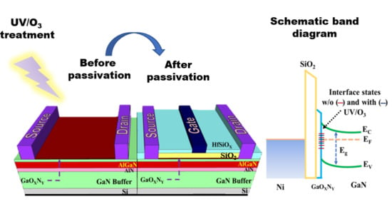
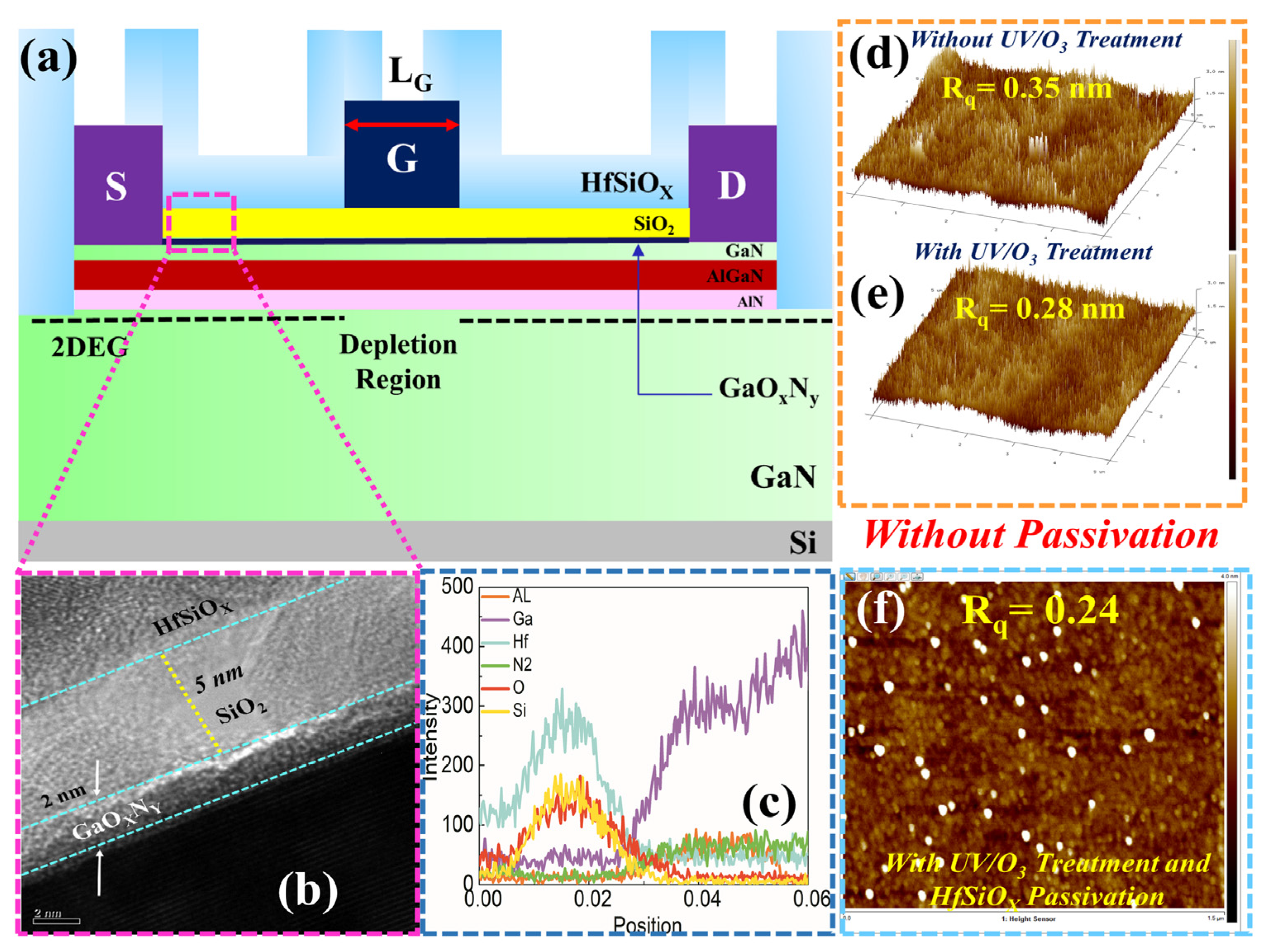
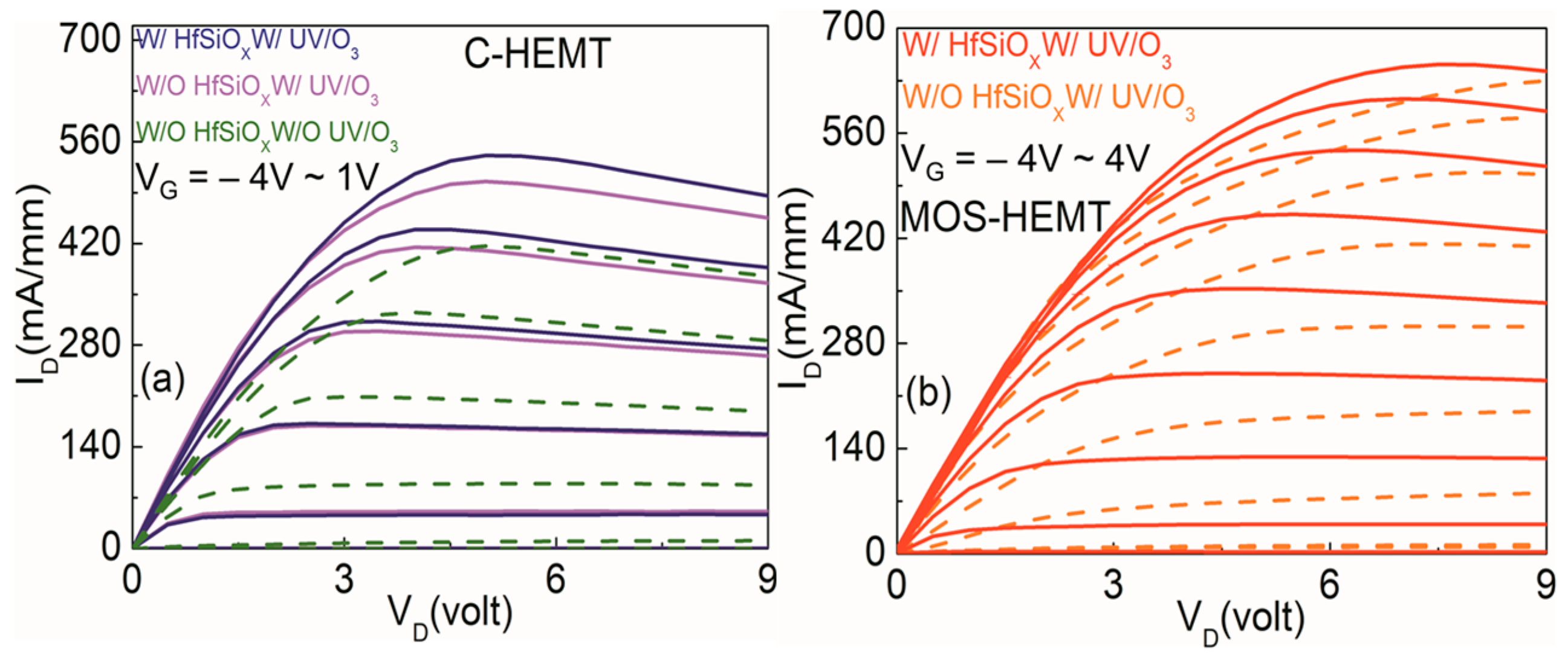
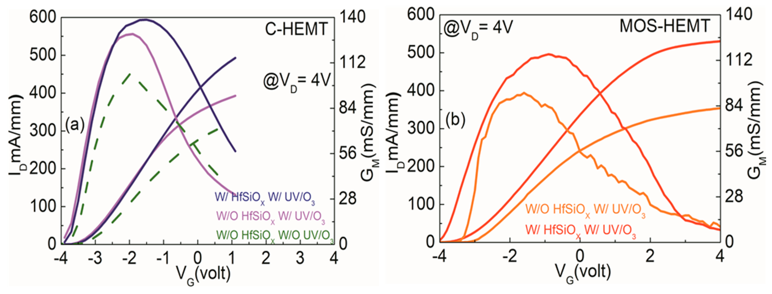
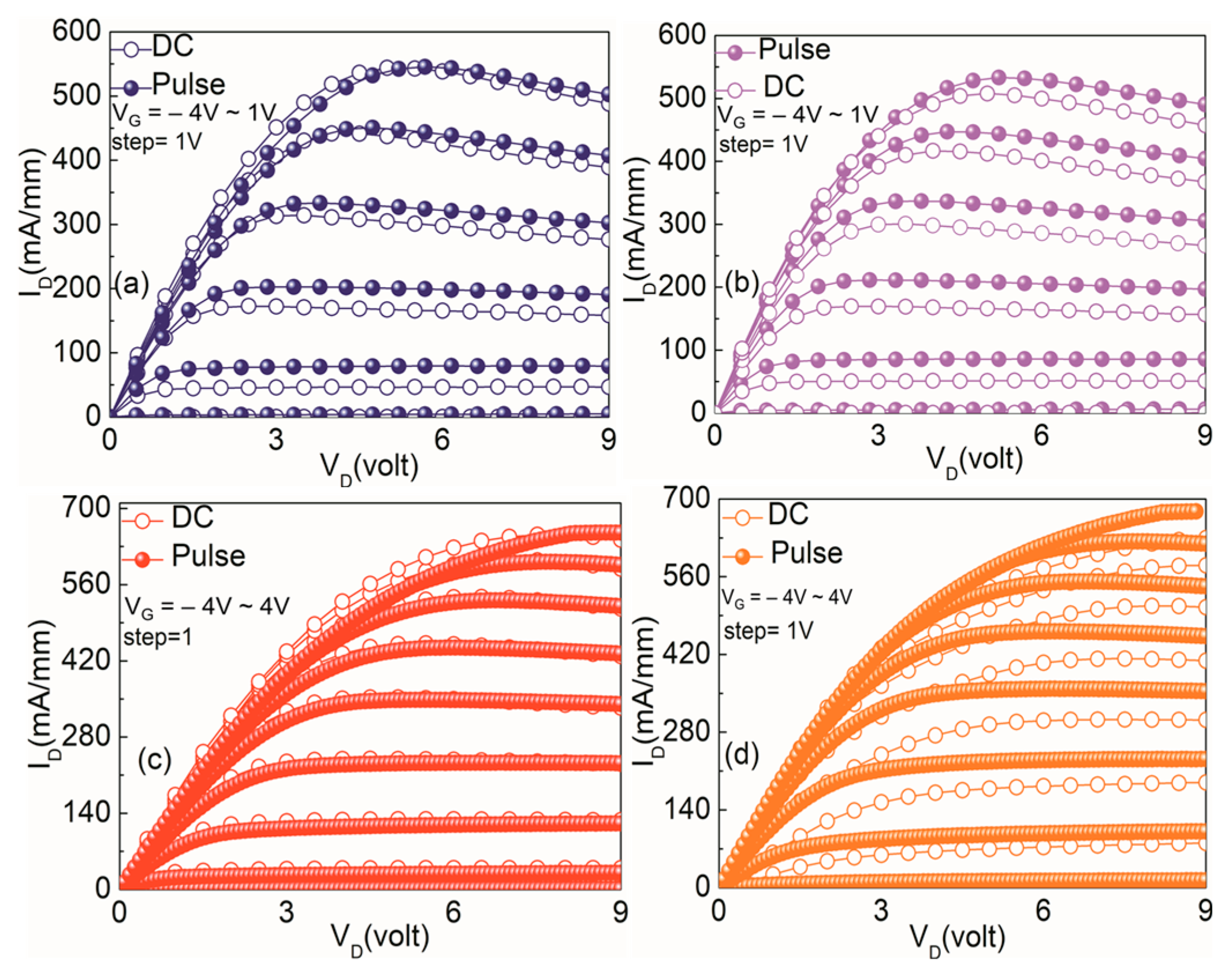
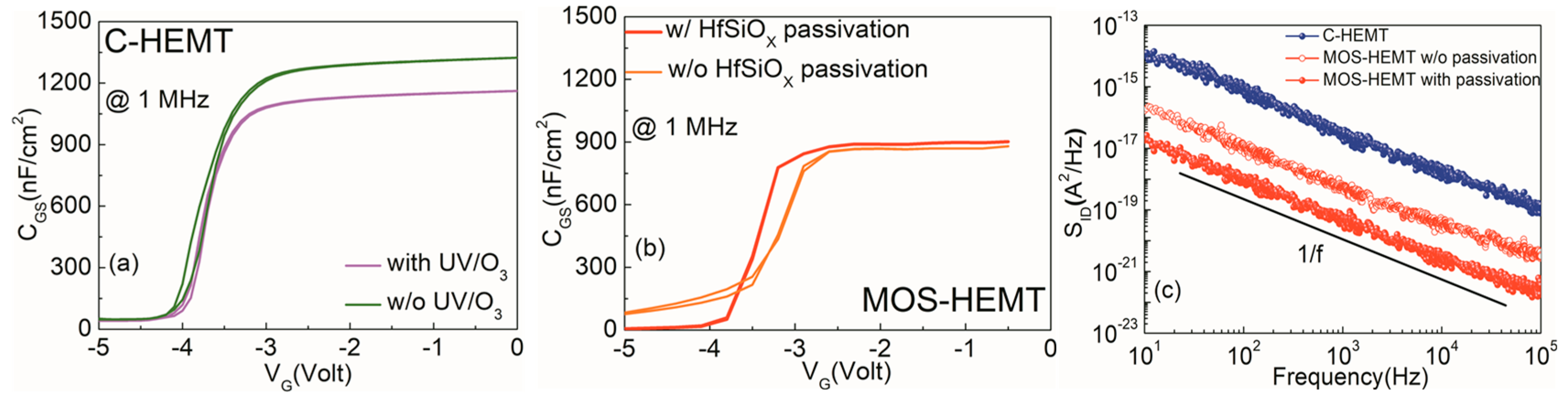
3. Results and Discussion

Figure 1b shows the transmission electron microscopy (TEM) image of the UV/O3 surface-treated HfSiOX-passivated MOS-HEMT. From TEM image, it can be understood that, due to the UV/O3 surface treatment prior to gate dielectric deposition, a thin layer of GaOXNY was formed [25]. The energy dispersive X-ray (EDX) line scan of HfSiOX was shown in Figure 1c. Figure 1d,e shows the atomic force microscopy (AFM) images of the unpassivated sample with and without UV/O3 plasma treatment, while the AFM image of the UV/O3 modified HfSiOX passivated sample is shown in Figure 1f. The combined effects of UV/O3 surface treatment and the deposition of HfSiOX passivation layer decreased the surface roughness significantly, which subsequently improved the device performance.
To analyse the improvement of device performance, X-ray photoelectron spectroscopy (XPS) was performed using K-Alpha X-ray photoelectron spectrometer to examine the change in the surface chemistry of the SiO2/GaN interface after UV/O3 plasma treatment. Figure 2a,b exhibit the change in atomic composition of GaN 3d core levels without and with UV/O3 surface treatment, respectively. It can be seen that both spectra were de-convoluted into Ga-N and Ga-O peaks. The Ga-N peak de-convoluted at 19.7 eV and Ga-O peak appeared at 20.8 eV, considering spin orbital splitting [15]. The peak intensity ratio of Ga-O/Ga-N was improved to 75% from 38% after UV/O3 plasma treatment, indicating an improved passivation. Since the standard Gibbs free energy of the Ga-O bond is negatively larger (−285 kJ/mol) than Ga-N bond (−157 kJ/mol), the Ga atoms in the Ga-O bond could come from the Ga-N bond [15].
The typical drain current-voltage characteristics of the UV/O3 surface-treated MOS-HEMT and C-HEMT before and after HfSiOX passivation is shown in Figure 3. The maximum drain currents (IDMAX) (@ VG = 4 V) before/after passivation were found to be 655/620 mA/mm for MOS-HEMT and 542/504 mA/mm (@ VG = 1 V) for C-HEMT, respectively. Owing to the large gate leakage current, C-HEMT could not be biased with high VG. Henceforth, the reduction of IDMAX in C-HEMT was due to the large gate leakage current [26]. The improvement of the IDMAX after passivation was attributed to the increase in sheet electron concentration [27] and surface-controlled effect [28]. After passivation, the SiO2 MOS-HEMT showed good pinch-off characteristics. In comparison, IDMAX was found approximately to be 415 mA/mm for C-HEMT without surface treatment and passivation.
To understand the gate controllability of UV/O3 surface-modified MOS-HEMT and C-HEMT, the transfer characteristics were calibrated before and after passivation at VD = 4 V, as shown in Figure 4. The threshold voltage (VTH) is defined as the gate bias intercept point of the linear extrapolation of ID at peak transconductance (GMMAX) [29]. VTH of the MOS-HEMT after and before passivation were found to be −3.0 V and −2.65 V, respectively. For C-HEMT, VTH was found to be approximately −3.05 V before passivation, which is hardly a change after HfSiOX passivation. In previous literature, the negative shifting of VTH in MOS-HEMT compared to planar HEMT was observed due to the larger separation between the gate and the channel [30]. The threshold voltage can be expressed as [31]
V t h = ϕ B Δ E C ϕ F t o x ε o x ( P 1 + P 2 + P 3 + q n G a N / S i O 2 ) t c a p ε c a p ( P 2 + P 3 ) t b ε b P 3 q n o x 2 ε o x t o x 2
where B is the metal barrier height ;   F is the energy difference EC−EF (EF is the Fermi energy) in the GaN bulk; Δ E c is the conduction band offset between SiO2 and GaN; t b is the barrier thickness; t o x is the SiO2 thickness; ε b is the permittivity of the barrier layer; ε o x is the permittivity of the SiO2; n o x is the oxide charge ;   n G a N / S i O 2 is the interface charge density at the SiO2/GaN interface; and P 1 , P 2 ,   and   P 3 are the total polarization sheet charges (sum of the spontaneous and piezoelectric polarization) at the GaN-cap surface, GaN-cap/AlGaN interface, and AlGaN/GaN buffer interface, respectively. The UV/O3 treatment could screen internal/external polarization bound charges and form thin Ga2OX layer on the GaN surface that could shift the VTH towards positive [16]. Another reason for the positive shifting of threshold voltage in the MOS-HEMT might be the band bending at the SiO2/GaN interface, which changed the Δ E C causing the UV-O3 treatment [11]. After HfSiOX passivation, the sheet carrier concentration was increased in the channel, which effectively shifted the VTH in the negative direction [32].
GMMAX was increased to 116 mS/mm after passivation from 90 mS/mm for MOS-HEMT, while for UV/O3-treated C-HEMT, the GMMAX was increased to 138 mS/mm (129 mS/mm) after passivation (before passivation) treatment. To understand the linear behaviour of the devices, the gate voltage swing (GVS) was calculated for two devices. The GVS, defined as 10% drop from the GMMAX, was increased to 2.53 V (1.55 V) from 1.60 V (1.15 V) for MOS-HEMT (C-HEMT) after passivation [30]. The largest GVS after passivation suggests a better linear behaviour for the UV/O3 surface-treated MOS-HEMT compared with the C-HEMT, from which a smaller intermodular distortion, a smaller phase noise, and a larger dynamic range could be expected, thus making it desirable for practical amplifier applications [30]. The GMMAX and GVS were found to be 104 mS/mm and 0.87 V, respectively, for C-HEMT without UV/O3 treatment as well as HfSiOX passivation.
Figure 5a shows the subthreshold characteristics as a function of gate voltage (@ VD = 4 V) for UV/O3 surface-treated MOS-HEMT and C-HEMT after passivation. It is clearly found that the subthreshold drain leakage current was decreased more than two orders of magnitude in UV/O3 surface modified HfSiOX passivated MOS-HEMT than C-HEMT. The interface oxide (GaOXNY) on the GaN, formed by the UV/O3 surface treatment, reduced the defect states at the metal–semiconductor interfaces resulting in the reduction of subthreshold drain leakage current and the reverse-biased gate leakage current in MOS-HEMT as shown in Figure 5a [15]. The subthreshold drain leakage current is dominated by the reverse-biased drain leakage current in the pinch-off region [33]. Since the reverse bias gate leakage current was suppressed in MOS-HEMT, the subthreshold drain leakage was decreased due to the improvement of the metal barrier height, as discussed later [34]. The subthreshold swing (SS) was also highly dependent on the reversed-bias gate leakage current [33]. The SS is defined as [35]
S S = ( l o g I D S V G S ) 1
To understand the gate controllability, the SS values of the MOS-HEMT and C-HEMT were calculated from Figure 5a. Plasma-treated MOS-HEMT after passivation exhibited much lower SS of 85 mV/dec than for C-HEMT (125 mV/dec). The ON/OFF ratio (ION/IOFF) for MOS-HEMT was found to be approximately 3.1 × 10 7 , while for C-HEMT it was found to be 1.6 × 10 6 . The SS and ION/IOFF were found to be 160 mV/dec and 4.8 × 10 5 for C-HEMT without UV/O3 treatment and HfSiOX passivation.
The reverse and forward gate leakage I-V characteristics of the surface-treated SiO2 MOS-HEMT and C-HEMT after passivation are shown in Figure 5a. It was clearly revealed that the reverse gate leakage current (IG) (@ VG = −15 V) of MOS-HEMT was 9.1 × 10 10 A/mm, which was nearly two orders of magnitude less than C-HEMT (4.3 × 10 8 A/mm). As expected, due to the increment of effective barrier height, causing the insertion of large band gap (~9 eV) ALD SiO2 as gate dielectric, the gate leakage current was reduced in MOS-HEMT compared to C-HEMT. The band alignment of Ni/SiO2/GaN Schottky interface with Ga-O interlayer due to UV/O3 surface treatment might be another reason for the noticeable reduction of IG [15].
The ideality factor ( η ) can be extracted by employing the standard thermionic equation as [36]
η =       q k T ( d V d ( l n I ) )
where T is the temperature, q is the electron charge, k is the Boltzmann constant, and V is the applied voltage.
The ideality factors of 2.5 and 3.2 were calculated for MOS-HEMT and C-HEMT, respectively. The UV/O3 surface plasma treatment prior to gate dielectric deposition reduced the interface state densities, which effectively improved the ideality factor of the MOS-HEMT. Furthermore, a higher turn on voltage (VT) was observed in C-HEMT with UV/O3 surface treatment and MOS-HEMT, as shown in the inset of Figure 5a. The shift of VT was associated with the formation of Ga-O interface oxide layer by UV/O3 surface treatment in C-HEMT [15].
Figure 5b shows the hysteresis characteristics for MOS-HEMT and C-HEMT before and after HfSiOX passivation (@ VD = 6 V). The MOS-HEMT exhibited less hysteresis than C-HEMT after HfSiOX passivation. The combined effects of UV/O3 surface treatment and HfSiOX passivation resulted in the significant reduction of hysteresis in SiO2-MOS-HEMT. Compared to C-HEMT, the MOS-HEMT exhibited almost low hysteresis of 0.11 V after passivation due to the effective neutralization of the surface caused by the Ga-O interface oxide passivation [15] and HfSiOX passivation layer [35]. Due to the presence of acceptor-like surface states on the device, counter-clockwise hysteresis was found [35].
To investigate the effectiveness of the HfSiOX surface passivation and UV/O3 surface treatment in the MOS-HEMT compared to C-HEMT, the gate lag measurements were employed. Figure 6a–d show the drain current response of the UV/O3-treated MOS-HEMT and C-HEMT before and after HfSiOX passivation. The pulse width and pulse period are set to 500 µs and 50 ms, respectively. From observation, it was clearly revealed that with HfSiOX passivation the current collapse was improved significantly in MOS-HEMT over C-HEMT. The drain-source current collapse was significantly improved to 0.6% (7%) in MOS-HEMT (C-HEMT) after HfSiOX passivation, while before passivation it was found to be approximately 10% (13%) (@ VD = 8 V, VG = 0 V). Most of the surface traps presented in the S/D access regions might have been passivated by UV/O3 surface modification and HfSiOX passivation, resulting in significant improvement in the current collapse. Without surface treatment and passivation, the current collapse was found in C-HEMT to be approximately 20% (not shown here). The formation of the thin Ga-O interface layer between gate metal and GaN cap, which serves as the passivation layer, resulted in the reduction of current collapse to 13% from 20% in C-HEMT [15,37].
In order to understand the reduction of trap states after the UV/O3 surface treatment and HfSiOX passivation of the devices, capacitance-voltage (C-V) measurements of C-HEMT and MOS-HEMT were measured at 1 MHz, shown in Figure 7a,b. The interface state density (Dit) for surface-treated MOS-HEMT can be extracted from the previously reported formula [38] to be 1.9   × 10 12   eV 1 · cm 2   ( 4.1   × 10 12   eV 1 · cm 2 ) with HfSiOX passivation (without passivation). To realize the surface passivation effects on the reduction of interface state density, Dits for C-HEMT were also estimated to be 9.7   × 10 12   eV 1 · cm 2   ( 1.4 × 10 13   eV 1 · cm 2 ) after (before) HfSiOX surface passivation. A similar trend was found in the previous report [39]. Due to the combined effects of UV/O3 surface treatment and HfSiOX passivation, the interface trap density was reduced approximately one order of magnitude in MOS-HEMT compared to C-HEMT.
Low-frequency noise, or 1/f measurement, is an effective method for studying electron-trapping and -de-trapping behaviour. Figure 7c shows the low-frequency characteristics, measured at VDS = 4 V, VGS = −1 V, and f = 10~105 Hz, for MOS-HEMT before and after passivation, and C-HEMT. In 1/f-noise characteristics, the variation of noise current spectral density SID (A2/Hz) with frequency was measured. This is directly related to the presence of electron traps and/or de-trapping between the 2 DEG channel and traps in the GaN buffer layer [34]. It was found that SID of the MOS-HEMT was one order lower after passivation than before passivation, as expected from the improved surface quality [34]. Table 1 shows the comparison of MOS-HEMT and C-HEMT before and after UV/O3 modification and HfSiOX passivation.

4. Conclusions

In summary, we have demonstrated the combined effects of UV/O3 plasma treatment and the surface passivation using ALD-grown HfSiOX on the DC performance of SiO2-MOS-HEMTs. A high-quality HfSiOX passivation layer significantly reduced the current degradation from 10% to 0.6% in MOS-HEMT compared to C-HEMT by decreasing the trapping phenomenon originating from the surface states. A significant enhancement of electrical characteristics in MOS-HEMT was observed after the combined treatment, compared to C-HEMT. The MOS-HEMT with surface plasma treatment after passivation exhibited IDMAX of 655 mA/mm, GMMAX of 116 mS/mm, on-off ratio of 3.1 × 10 7 with subthreshold slope of 85 mV/dec, and VTH of −3 V. The combined effects of band bending at the SiO2/GaN interface and screening of internal/external-polarization-bound charges by the UV/O3 surface treatment shifted the VTH in a positive direction in MOS-HEMT, compared to C-HEMT. The reversed gate leakage current of approximately 9.1 × 10 10 A/mm was achieved. Furthermore, the aforementioned combined treatment decreased the interface trap states from 4.1   × 10 12 eV 1 · cm 2 to 1.9 × 10 12 eV 1 · cm 2 in UV/O3-treated MOS-HEMT after HfSiOX passivation, which resulted in the reduction of hysteresis and 1/f-noise characteristics, compared to C-HEMT. The experimental results are significant for the development of high-performance GaN-based MOS-HEMT.

Author Contributions

S.M. is responsible for the device preparation and characterization, data analysis, and paper writing. All authors analyzed the data and revised the manuscript. Y.-H.W. is the advisor to monitor the progress and paper editing. All authors have read and agreed to the published version of the manuscript.

Funding

“This research was funded by Ministry of Science and Technology, Taiwan, grant number MOST 106-2221-E-006-219-MY3 and MOST 109-2221-E-06-075-MY2” and Transcom. Inc., Taiwan, grant number 109S0172.

Acknowledgments

The flicker noise measurements in Taiwan Semiconductor Research Institute, National Applied Research Laboratories, Taiwan are highly appreciated.

Conflicts of Interest

The Authors declare no conflict of interest.

References

  1. Borga, M.; Meneghini, M.; Benazzi, D.; Canato, E.; Püsche, R.; Derluyn, J.; Abid, I.; Medjdoub, F.; Meneghessoa, G.; Zanoni, E. Buffer breakdown in GaN-on-Si HEMTs: A comprehensive study based on a sequential growth experiment. Microelectron. Reliab. 2019, 100–101, 1–5. [Google Scholar] [CrossRef]
  2. Ardaravičius, L.; Matulionis, A.; Liberis, J.; Kiprijanovic, O.; Ramonas, M.; Eastman, L.F.; Shealy, J.R.; Vertiatchikh, A. Electron drift velocity in AlGaN/GaN channel at high electric fields. Appl. Phys. Lett. 2003, 83, 4038–4040. [Google Scholar] [CrossRef]
  3. Mazumder, S.; Wang, Y.H. Investigation of HfSiOX passivation effect on AlGaN/GaN HEMT. In Proceedings of the 2020 International Symposium on Devices, Circuits and Systems, ISDCS, Howrah, India, 4–6 March 2020; pp. 1–4. [Google Scholar]
  4. Hori, Y.; Yatabe, Z.; Hashizume, T. Characterization of interface states in Al2O3/AlGaN/GaN structures for improved performance of high-electron-mobility transistors. J. Appl. Phys. 2013, 114, 244503. [Google Scholar] [CrossRef] [Green Version]
  5. Arulkumaran, S. Surface passivation effects in AlGaN/GaN HEMTs on high-resistivity Si substrate. In Proceedings of the 2007 International Workshop on Physics of Semiconductor Devices, IWPS, Mumbai, India, 16–20 December 2007; pp. 317–322. [Google Scholar]
  6. Eller, B.S.; Yang, J.; Nemanich, R.J. Electronic surface and dielectric interface states on GaN and AlGaN. J. Vac. Sci. Technol. A 2013, 31, 050807. [Google Scholar] [CrossRef]
  7. Jussila, H.; Mattila, P.; Oksanen, J.; Perros, A.; Riikonen, J.; Bosund, M.; Varpula, A.; Huhtio, T.; Lipsanen, H.; Sopanen, M. High-k GaAs metal insulator semiconductor capacitors passivated by ex-situ plasma-enhanced atomic layer deposited AlN for fermi-level unpinning. Appl. Phys. Lett. 2012, 100, 071606. [Google Scholar] [CrossRef] [Green Version]
  8. Passlack, M.; Hong, M.; Mannaerts, J.P. Quasistatic and high frequency capacitance-voltage characterization of Ga2O3-GaAs structures fabricated by in-situ molecular beam epitaxy. Appl. Phys. Lett. 1996, 68, 1099–1101. [Google Scholar] [CrossRef]
  9. Park, S.; Kim, S.Y.; Choi, Y.; Kim, M.; Shin, H.; Kim, J.; Choi, W. Interface properties of atomic-layer-deposited Al2O3 thin films on ultraviolet/ozone-treated multilayer MoS2 crystals. ACS Appl. Mater. Interfaces 2016, 8, 11189–11193. [Google Scholar] [CrossRef]
  10. Smith, L.L.; King, S.W.; Nemanich, R.J.; Davis, R.F. Cleaning of GaN surfaces. J. Electron. Mater. 1996, 25, 805–810. [Google Scholar] [CrossRef]
  11. Bradley, S.T.; Goss, S.H.; Hwang, J.; Schaff, W.J.; Brillson, L.J. Surface cleaning and annealing effects on Ni/AlGaN interface atomic composition and schottky barrier height. Appl. Phys. Lett. 2004, 85, 1368–1370. [Google Scholar] [CrossRef]
  12. Kim, K.; Ryu, J.H.; Kim, J.; Cho, S.J.; Liu, D.; Park, J.; Lee, I.-K.; Moody, B.; Zhou, W.; Albrecht, J.; et al. Band-bending of Ga-polar GaN interfaced with Al2O3 through ultraviolet/ozone treatment. ACS Appl. Mater. Interfaces 2017, 9, 17576–17585. [Google Scholar] [CrossRef]
  13. Choi, J.H.; Cho, C.H.; Cha, H.Y. Design consideration of high voltage Ga2O3 vertical Schottky barrier diode with field plate. Results Phys. 2018, 9, 1170–1171. [Google Scholar] [CrossRef]
  14. Liu, X.; Low, E.K.F.; Pan, J.; Liu, W.; Teo, K.L.; Tan, L.S.; Yeo, Y.C. Impact of in situ vacuum anneal and SiH4 treatment on electrical characteristics of AlGaN/GaN metal-oxide-semiconductor high-electron mobility transistors. Appl. Phys. Lett. 2011, 99, 093504. [Google Scholar] [CrossRef]
  15. Kim, K.; Liu, D.; Gong, J.; Ma, Z. Reduction of leakage current in GaN Schottky diodes through ultraviolet/ozone plasma treatment. IEEE Electron. Device Lett. 2019, 40, 1796–1799. [Google Scholar] [CrossRef]
  16. Kim, K.; Kim, T.J.; Zhang, H.; Liu, D.; Jung, Y.H.; Gong, J.; Ma, Z. AlGaN/GaN schottky-gate HEMTs with UV/O3-treated gate interface. IEEE Electron. Device Lett. 2020, 41, 1488–1491. [Google Scholar] [CrossRef]
  17. Arulkumaran, S.; Egawa, T.; Ishikawa, H.; Jimbo, T.; Sano, Y. Surface passivation effects on AlGaN/GaN high-electron-mobility transistors with SiO2, Si3N4, and silicon oxynitride. Appl. Phys. Lett. 2003, 84, 613–615. [Google Scholar] [CrossRef]
  18. Javorka, P.; Bernat, J.; Fox, A.; Marso, M.; Lüth, H.; Kordoš, P. Influence of SiO2 and Si3N4 passivation on AlGaN/GaN/Si HEMT performance. Electron. Lett. 2003, 39, 1155–1157. [Google Scholar] [CrossRef]
  19. Huang, S.; Jiang, Q.; Yang, S.; Zhou, C.; Chen, K.J. Effective passivation of AlGaN/GaN HEMTs by ALD-grown AlN thin film. IEEE Electron. Device Lett. 2012, 33, 516–518. [Google Scholar] [CrossRef]
  20. Lin, Y.S.; Lin, S.F.; Hsu, W.C. Microwave and power characteristics of AlGaN/GaN/Si high-electron mobility transistors with HfO2 and TiO2 passivation. Semicond. Sci. Technol. 2015, 30, 015016. [Google Scholar] [CrossRef]
  21. Li, S.; Hu, Q.; Wang, X.; Li, T.; Li, X.; Wu, Y. Improved interface properties and dielectric breakdown in recessed AlGaN/GaN MOS-HEMTs using HfSiOX as gate dielectric. IEEE Electron. Device Lett. 2019, 40, 295–298. [Google Scholar] [CrossRef]
  22. Chan, S.H.; Tahhan, M.; Liu, X.; Bisi, D.; Gupta, C.; Koksaldi, O.; Li, H.; Mates, T.; Denbaars, S.P.; Keller, S. Metalorganic chemical vapor deposition and characterization of (Al,Si)O dielectrics for GaN-based devices. Jpn. J. Appl. Phys. 2016, 55, 021501. [Google Scholar] [CrossRef]
  23. Karim, Z.; Boissiere, O.; Lohe, C.; Zhang, Z.; Manke, C.; Lehnen, P.; Baumann, P.K.; Dalton, J.; Park, W.; Ramanathan, S.; et al. Advanced metal gate electrode options compatible with ALD and AVD® HfSiOx based gate dielectrics. ECS Trans. 2006, 3, 363–374. [Google Scholar] [CrossRef]
  24. Yang, W.; Fronk, M.; Geng, Y.; Chen, L.; Sun, Q.Q.; Gordan, O.D.; Zhou, P.; Zahn, D.R.; Zhang, D.W. Optical properties and bandgap evolution of ALD HfSiOx films. Nanoscale Res. Lett. 2015, 10, 1–5. [Google Scholar] [CrossRef] [PubMed] [Green Version]
  25. Hou, B.; Ma, X.; Zhu, J.; Yang, L.; Chen, W.; Mi, M.; Zhu, Q.; Chen, L.; Zhang, R.; Zhang, M.; et al. 0.9-A/mm, 2.6-V flash-like normally-off Al2O3/AlGaN/GaN MIS-HEMTs using charge trapping technique. IEEE Electron. Device Lett. 2018, 39, 397–400. [Google Scholar] [CrossRef]
  26. Zheng, Y.Y.; Yue, H.; Cheng, Z.J.; Qian, F.; Yu, N.J.; Hua, M.X. A study on Al2O3 passivation in GaN MOS-HEMT by pulsed stress. Chin. Phys. B 2008, 17, 1405. [Google Scholar] [CrossRef]
  27. Lin, Y.S.; Lin, S.F. Large-signal linearity and high-frequency noise of passivated AlGaN/GaN high-electron mobility transistors. Micromachines 2021, 12, 1–7. [Google Scholar]
  28. Kikkawa, T.; Nagahara, M.; Okamoto, N.; Tateno, Y.; Yamaaguchi, Y.; Hara, N.; Joshin, K.; Asbeck, P.M. Surface-charge controlled AlGaN/ GaN-power HFET without current collapse and Gm dispersion. IEDM Tech. Dig. 2001, 8, 585. [Google Scholar]
  29. Cai, Y.; Zhou, Y.; Lau, K.M.; Chen, K.J. Enhancement-mode AlGaN/GaN HEMTs with low on-resistance and low knee voltage. IEEE Trans. Electron. 2006, E89-C7, 1025–1030. [Google Scholar] [CrossRef]
  30. Yue, Y.; Hao, Y.; Zhang, J.; Ni, J.; Mao, W.; Feng, Q.; Liu, L. AlGaN/GaN MOS-HEMT with HfO2 dielectric and Al2O3 interfacial passivation layer grown by atomic layer deposition. IEEE Electron. Device Lett. 2008, 29, 838–840. [Google Scholar] [CrossRef]
  31. Tapajna, M.; Kuzmik, J. A comprehensive analytical model for threshold voltage calculation in GaN based metal-oxide-semiconductor high-electronmobility transistors. Appl. Phys. Lett. 2012, 100, 113509. [Google Scholar] [CrossRef]
  32. Lu, W.; Kumar, V.; Schwindt, R.; Piner, E.; Adesida, I. A comparative study of surface passivation on AlGaN/GaN HEMTs. Solid State Electron. 2002, 46, 1441–1444. [Google Scholar] [CrossRef]
  33. Liu, L.; Xi, Y.; Ahn, S.; Ren, F.; Gila, B.P.; Pearton, S.J.; Kravchenko, I.I. Characteristics of gate leakage current and breakdown voltage of AlGaN/GaN high electron mobility transistors after postprocess annealing. J. Vac. Sci. Technol. B Microelectron. Nanom. Struct. 2014, 32, 1–5. [Google Scholar] [CrossRef]
  34. Reddy, M.S.P.; Park, W.S.; Im, K.S.; Lee, J.H. Dual-surface modification of AlGaN/GaN HEMTs using TMAH and piranha solutions for enhancing current and 1/f-Noise Characteristics. IEEE J. Electron. Devices Soc. 2018, 6, 791–796. [Google Scholar] [CrossRef]
  35. Liu, H.Y.; Ou, W.C.; Hsu, W.C. Investigation of post oxidation annealing effect on H2O2-grown Al2O3/AlGaN/GaN MOSHEMTs. IEEE J. Electron. Devices Soc. 2016, 4, 358–364. [Google Scholar] [CrossRef]
  36. Mahajan, S.S.; Malik, A.; Laishram, R.; Vinayak, S. Performance enhancement of gate-annealed AlGaN/GaN HEMTs. J. Kor. Phys. Soc. 2017, 70, 533–538. [Google Scholar] [CrossRef]
  37. Tingting, Y.; Xinyu, L.; Yingkui, Z.; Chengzhan, L.; Ke, W.; Guoguo, L. Impact of UV/ozone surface treatment on AlGaN/GaN HEMTs. J. Semicond. 2009, 30, 124001. [Google Scholar] [CrossRef]
  38. Kalb, W.L.; Batlogg, B. Calculating the trap density of states in organic field-effect transistors from experiment: A comparison of different methods. Phys. Rev. B 2010, 81, 1–13. [Google Scholar] [CrossRef] [Green Version]
  39. Anderson, T.J.; Wheeler, V.D.; Shahin, D.I.; Tadjer, M.J.; Koehler, A.D.; Hobart, K.D.; Christou, A.; Kub, F.J.; Eddy, C.R., Jr. Enhancement mode AlGaN/GaN MOS high-electron-mobility transistors with ZrO2 gate dielectric deposited by atomic layer deposition. Appl. Phys. Exp. 2016, 9, 071003. [Google Scholar] [CrossRef]
Figure 1. (a) Schematic illustration and (b) TEM image of ultraviolet-ozone (UV/O3)-treated HfSiOX passivated metal-oxide semiconductor high-electron mobility transistors (MOS-HEMT). (c) EDX line scan of HfSiOX. AFM image of MOS-HEMT (d) without UV/O3, (e) with UV/O3 treatment before passivation, and (f) with UV/O3 treatment after passivation.
Crystals 11 00136 g001
Figure 2. X-ray photoelectron spectroscopy (XPS) measurements of Ga 3d core levels in (a) without UV/O3 and (b) with UV/O3 surface-treated GaN MOS-HEMT.
Crystals 11 00136 g002
Figure 3. Comparison of drain current-voltage (ID-VD) characteristics of (a) conventional HEMT (C-HEMT) (before and after UV/O3 treatment) and (b) MOS-HEMT with and without HfSiOX passivation.
Crystals 11 00136 g003
Figure 4. Comparison of transfer characteristics (ID-VG) (@ VD = 4 V) of (a) C-HEMT (before and after UV/O3 treatment) and (b) MOS-HEMT with and without HfSiOX passivation.
Crystals 11 00136 g004
Figure 5. Comparison of (a) subthreshold (@ VD = 4 V) and gate leakage (IG-VG) characteristics of C-HEMT (before and after UV/O3 treatment) and MOS-HEMT with HfSiOX passivation. (b) Hysteresis characteristics of (@ VD = 6 V) C-HEMT (before and after UV/O3 treatment) and MOS-HEMT with and without HfSiOX passivation.
Crystals 11 00136 g005
Figure 6. Comparison of pulsed ID-VD characteristics of UV/O3-treated C-HEMT (a) after and (b) before HfSiOX passivation and MOS-HEMT (c) after and (d) before HfSiOX passivation.
Crystals 11 00136 g006
Figure 7. Comparison of C-V characteristics of C-HEMT (a) with and without UV/O3 treatment, and (b) MOS-HEMT with and without HfSiOX passivation. (c) Flicker noise characteristics of MOS-HEMT with and without HfSiOX passivation, and C-HEMT without any treatment.
Crystals 11 00136 g007
Table 1. Comparison MOS-HEMT and C-HEMT with different conditions.
ParametersC-HEMTC-HEMT with UV/O3C-HEMT with UV/O3 and HfSiOXMOS-HEMT with UV/O3MOS-HEMT with UV/O3 and HfSiOX
IDMAX (mA/mm)415504542620655
VTH (V)−3.1−3.05−3.05−2.65−3.0
GMMAX (mS/mm)10412913890116
SS (mV/dec)1601401259585
ION/IOFF4.8 × 10 5 ---1.6 × 10 6 ---3.1 × 10 7
IG (A/mm)
(@ VG = −15 V)
6.6 × 10 8 ---4.3 × 10 8 --- 9.1 × 10 10
Current collapse (%)20137100.6
Dit( e V 1 · c m 2 ) 2.1 × 10 13 1.4 × 10 13 9.7 × 10 12 4.1 × 10 12 1.9 × 10 12
Hysteresis (∆ V) (V)1.042.120.8041.950.11
GVS (V)0.871.151.551.602.53
Publisher’s Note: MDPI stays neutral with regard to jurisdictional claims in published maps and institutional affiliations.

