Rational Design of Binary Alloys for Catalytic Growth of Graphene via Chemical Vapor Deposition

 , ,
, ,
Abstract
: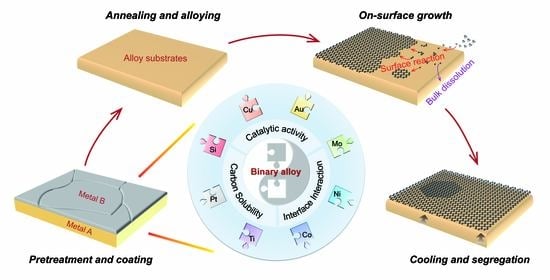
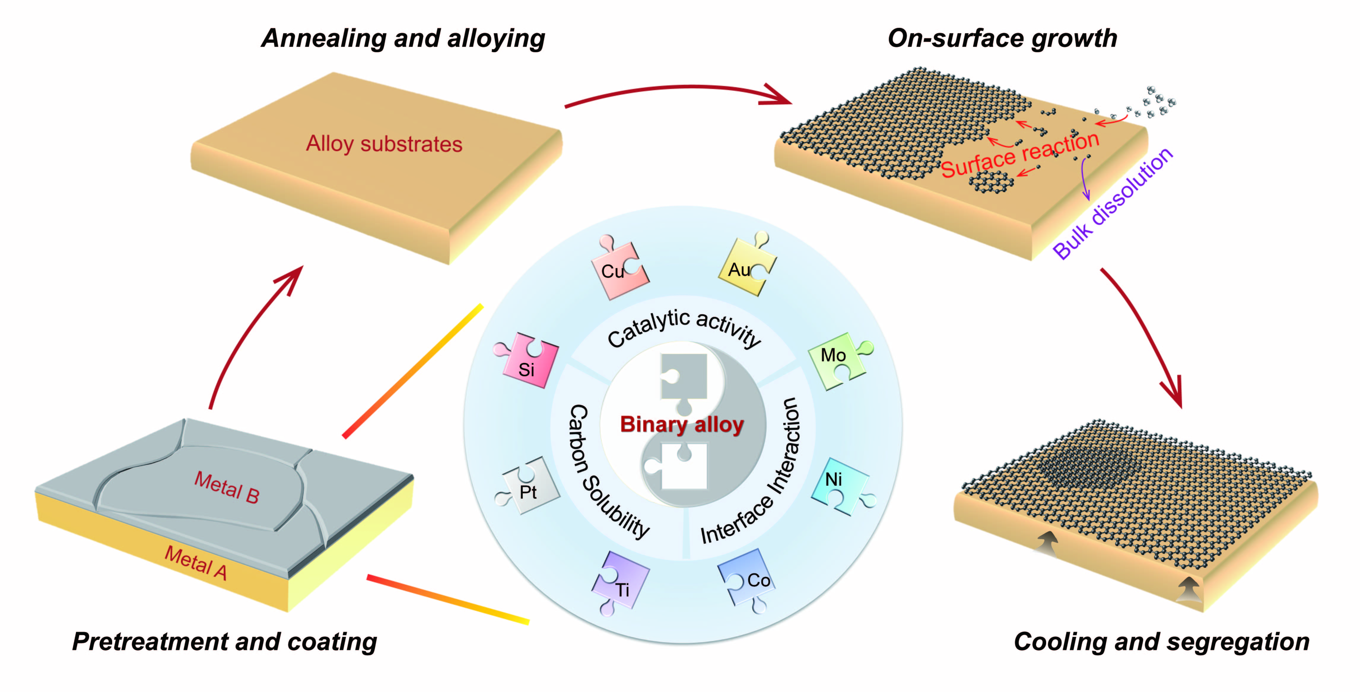
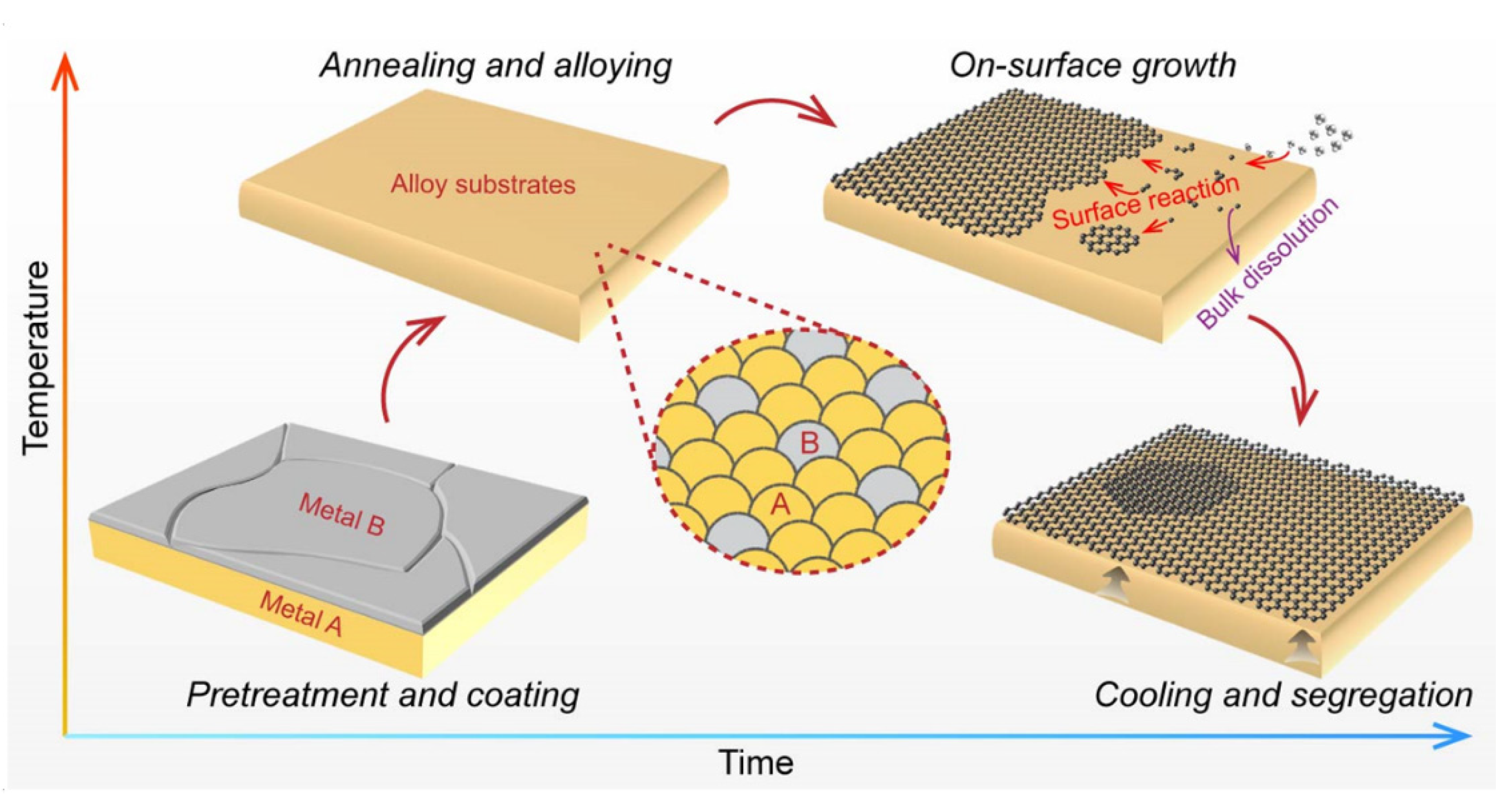
1. Introduction
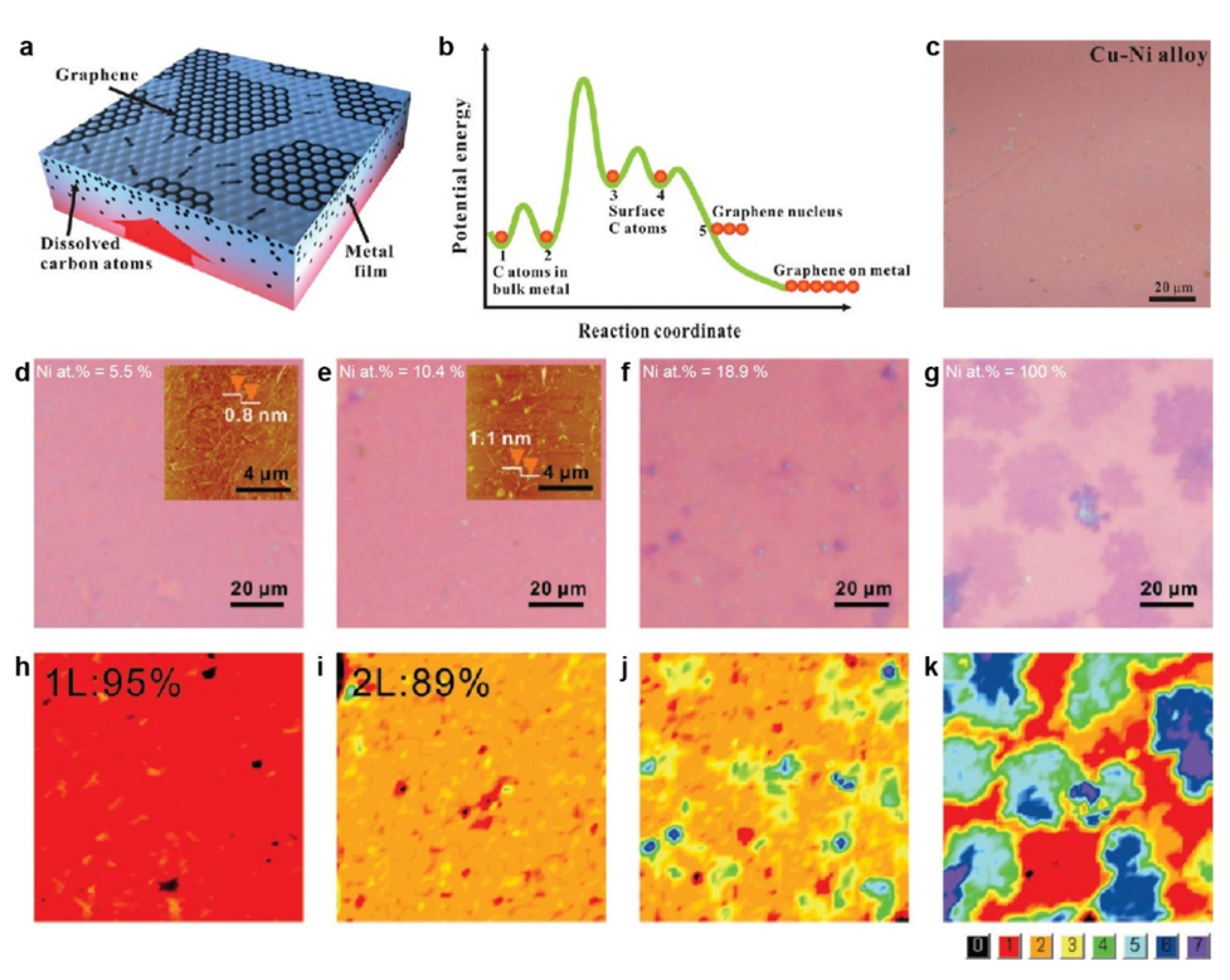
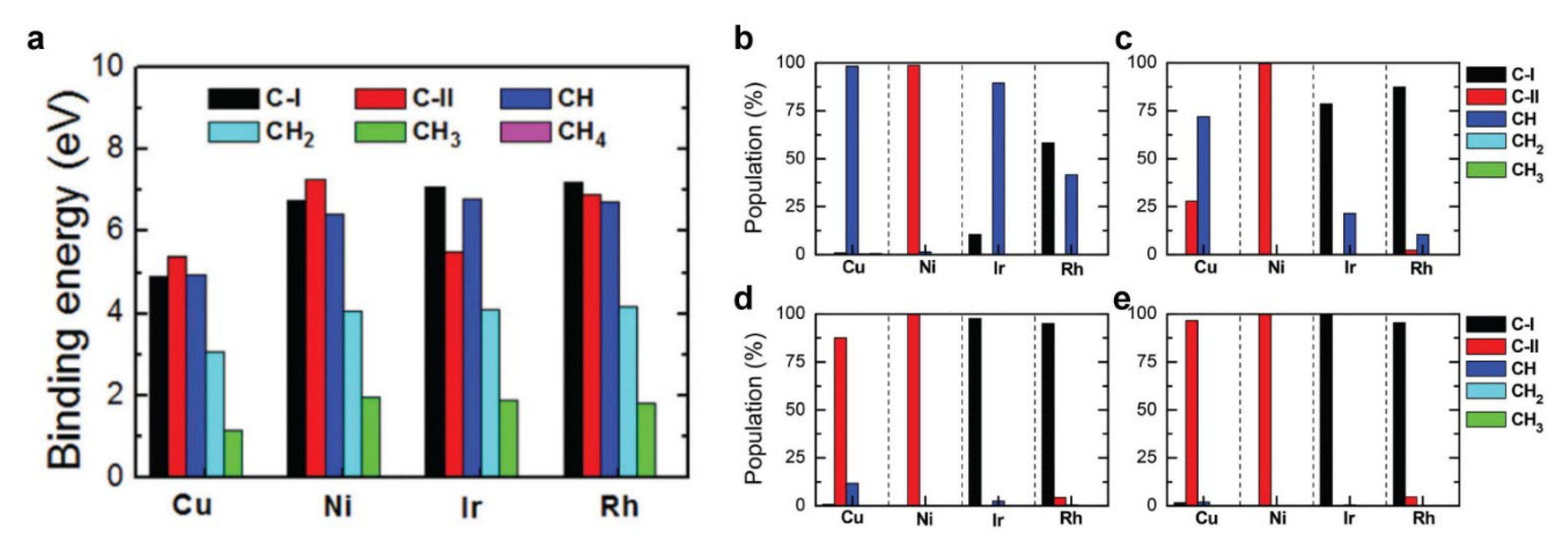
2. Elementary Steps for Graphene Growth on Metal Catalysts
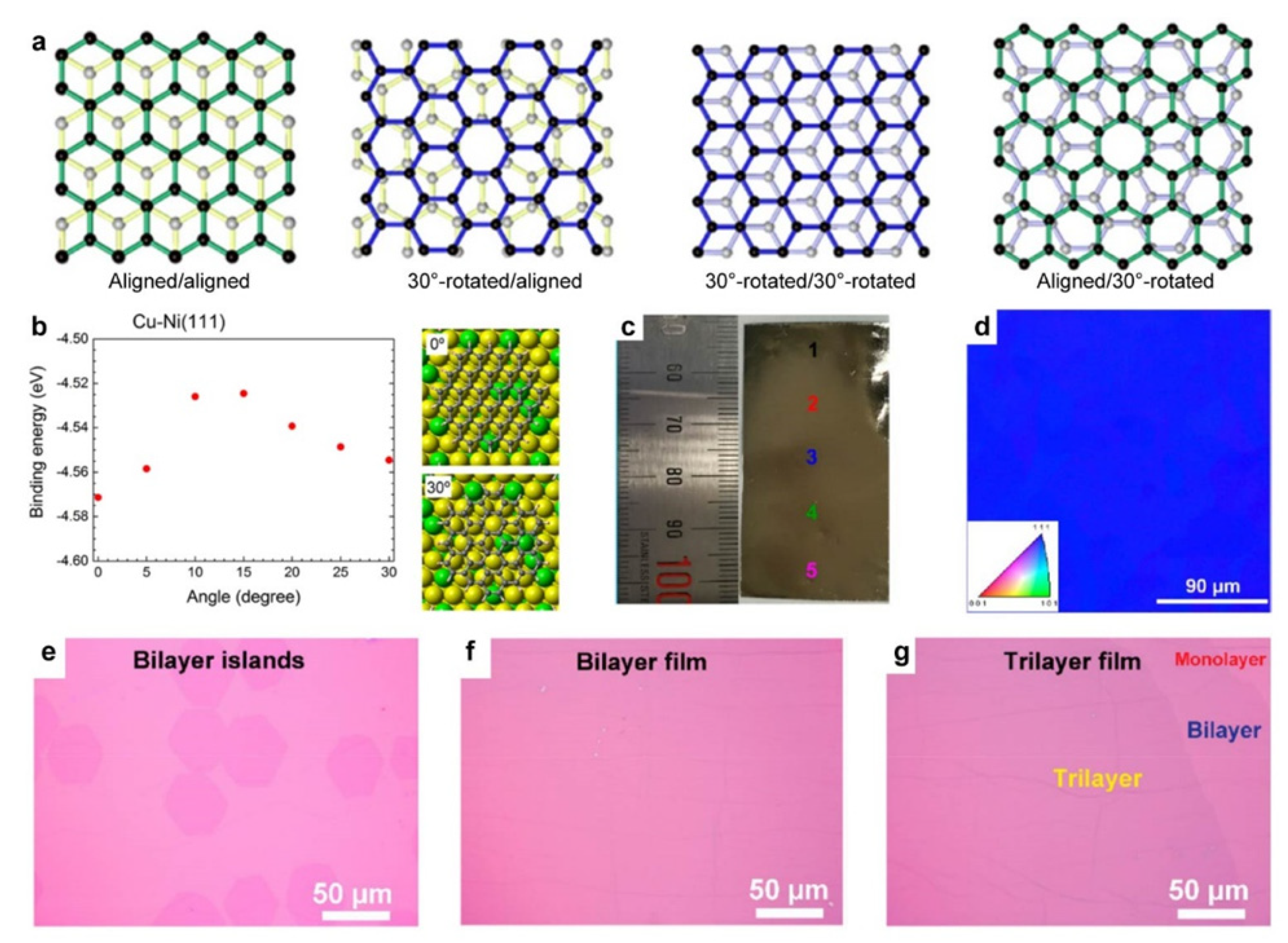
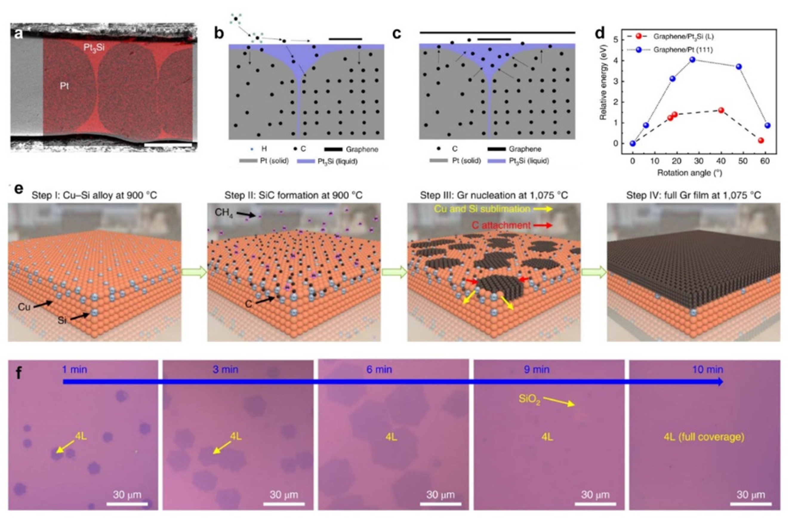
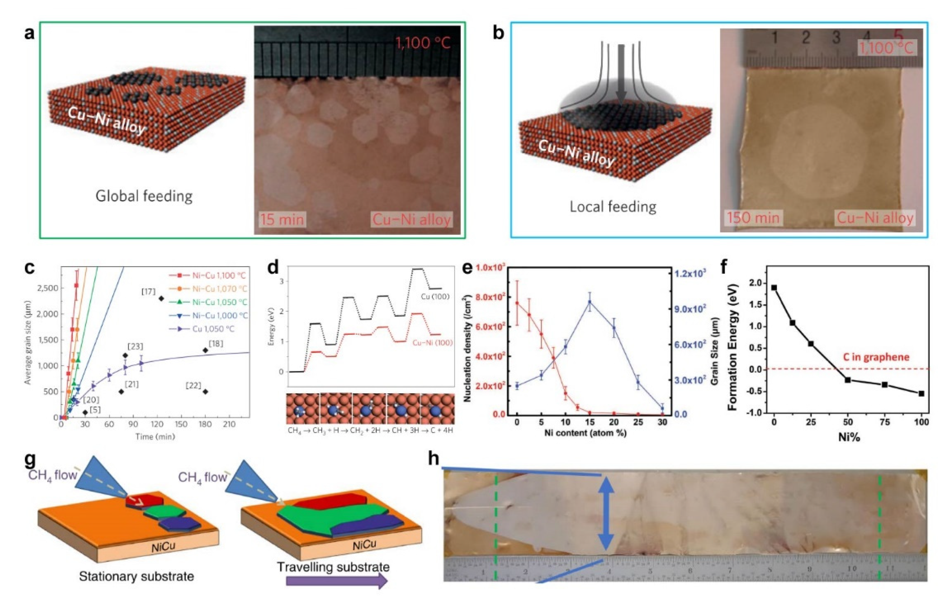
3. Layer Number Control of the Graphene Films
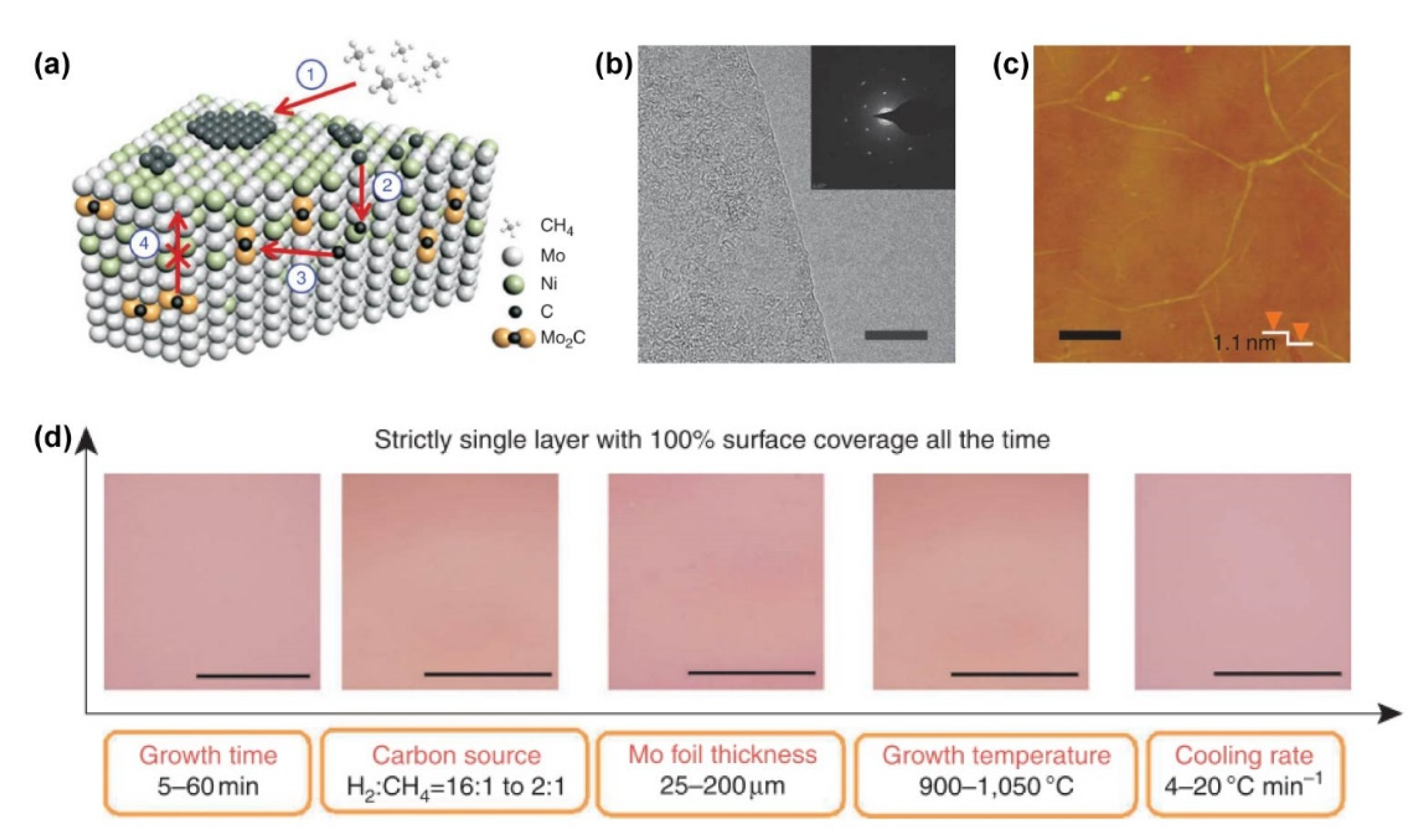
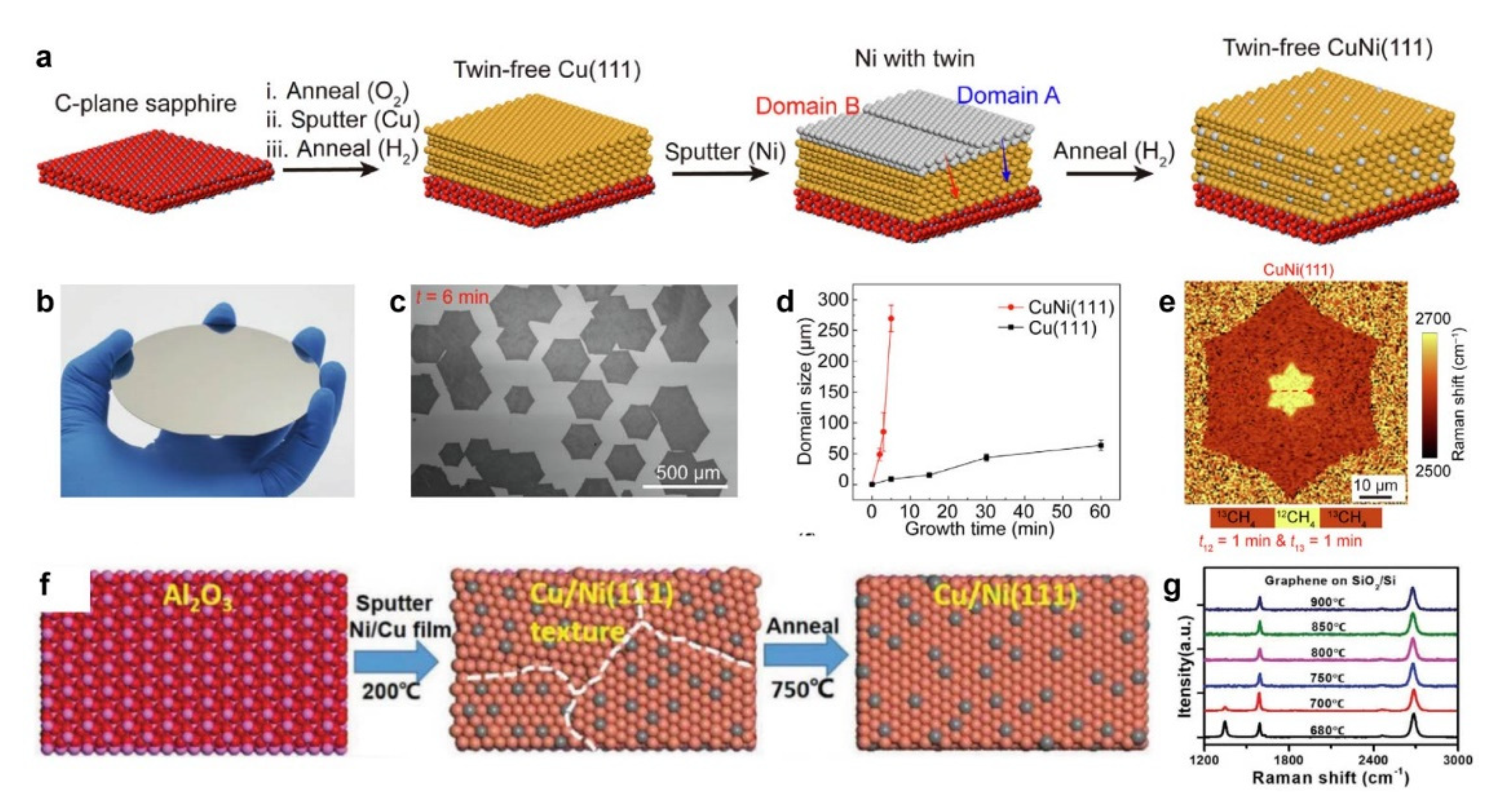
4. Low-Temperature and Fast Growth of Single-Crystal Graphene Films
5. Conclusions and Outlook
Author Contributions
Funding
Acknowledgments
Conflicts of Interest
References
- Novoselov, K.S.; Geim, A.K.; Morozov, S.V.; Jiang, D.; Zhang, Y.; Dubonos, S.V.; Grigorieva, I.V.; Firsov, A.A. Electric field effect in atomically thin carbon films. Science 2004, 306, 666–669. [Google Scholar] [CrossRef] [Green Version]
- Geim, A.K.; Novoselov, K.S. The rise of graphene. Nat. Mater. 2007, 6, 183–191. [Google Scholar] [CrossRef]
- Nair, R.R.; Blake, P.; Grigorenko, A.N.; Novoselov, K.S.; Booth, T.J.; Stauber, T.; Peres, N.M.R.; Geim, A.K. Fine structure constant defines visual transparency of graphene. Science 2008, 320, 1308. [Google Scholar] [CrossRef] [PubMed] [Green Version]
- Novoselov, K.S.; Jiang, Z.; Zhang, Y.; Morozov, S.V.; Stormer, H.L.; Zeitler, U.; Maan, J.C.; Boebinger, G.S.; Kim, P.; Geim, A.K. Room-temperature quantum hall effect in graphene. Science 2007, 315, 1379. [Google Scholar] [CrossRef] [PubMed] [Green Version]
- Novoselov, K.S.; Geim, A.K.; Morozov, S.V.; Jiang, D.; Katsnelson, M.I.; Grigorieva, I.V.; Dubonos, S.V.; Firsov, A.A. Two-dimensional gas of massless Dirac fermions in graphene. Nature 2005, 438, 197–200. [Google Scholar] [CrossRef] [PubMed]
- Du, X.; Skachko, I.; Duerr, F.; Luican, A.; Andrei, E.Y. Fractional quantum Hall effect and insulating phase of Dirac electrons in graphene. Nature 2009, 462, 192–195. [Google Scholar] [CrossRef] [Green Version]
- Bolotin, K.I.; Ghahari, F.; Shulman, M.D.; Stormer, H.L.; Kim, P. Observation of the fractional quantum Hall effect in graphene. Nature 2009, 462, 196–199. [Google Scholar] [CrossRef] [Green Version]
- Lee, C.; Wei, X.; Kysar, J.W.; Hone, J. Measurement of the elastic properties and intrinsic strength of monolayer graphene. Science 2008, 321, 385–388. [Google Scholar] [CrossRef]
- Balandin, A.A.; Ghosh, S.; Bao, W.; Calizo, I.; Teweldebrhan, D.; Miao, F.; Lau, C.N. Superior thermal conductivity of single-layer graphene. Nano Lett. 2008, 8, 902–907. [Google Scholar] [CrossRef]
- Bae, S.; Kim, H.; Lee, Y.; Xu, X.; Park, J.-S.; Zheng, Y.; Balakrishnan, J.; Lei, T.; Ri Kim, H.; Song, Y.I.; et al. Roll-to-roll production of 30-inch graphene films for transparent electrodes. Nat. Nanotechnol. 2010, 5, 574–578. [Google Scholar] [CrossRef] [Green Version]
- Schwierz, F. Graphene transistors. Nat. Nanotechnol. 2010, 5, 487–496. [Google Scholar] [CrossRef] [PubMed]
- Kim, K.; Choi, J.-Y.; Kim, T.; Cho, S.-H.; Chung, H.-J. A role for graphene in silicon-based semiconductor devices. Nature 2011, 479, 338–344. [Google Scholar] [CrossRef] [PubMed]
- Koppens, F.H.L.; Mueller, T.; Avouris, P.; Ferrari, A.C.; Vitiello, M.S.; Polini, M. Photodetectors based on graphene, other two-dimensional materials and hybrid systems. Nat. Nanotechnol. 2014, 9, 780–793. [Google Scholar] [CrossRef]
- Lin, L.; Deng, B.; Sun, J.; Peng, H.; Liu, Z. Bridging the gap between reality and ideal in chemical vapor deposition growth of graphene. Chem. Rev. 2018, 118, 9281–9343. [Google Scholar] [CrossRef]
- Yang, J. Towards large-scale and high-quality graphene films. Acta Phys. Chim. Sin. 2019, 35, 1043–1044. [Google Scholar] [CrossRef]
- Lin, L.; Peng, H.; Liu, Z. Synthesis challenges for graphene industry. Nat. Mater. 2019, 18, 520–524. [Google Scholar] [CrossRef] [PubMed]
- Li, X.; Cai, W.; An, J.; Kim, S.; Nah, J.; Yang, D.; Piner, R.; Velamakanni, A.; Jung, I.; Tutuc, E.; et al. Large-area synthesis of high-quality and uniform graphene films on copper foils. Science 2009, 324, 1312–1314. [Google Scholar] [CrossRef] [Green Version]
- Reina, A.; Jia, X.; Ho, J.; Nezich, D.; Son, H.; Bulovic, V.; Dresselhaus, M.S.; Kong, J. Large area, few-layer graphene films on arbitrary substrates by chemical vapor deposition. Nano Lett. 2009, 9, 30–35. [Google Scholar] [CrossRef]
- Zhang, Y.; Tang, T.-T.; Girit, C.; Hao, Z.; Martin, M.C.; Zettl, A.; Crommie, M.F.; Shen, Y.R.; Wang, F. Direct observation of a widely tunable bandgap in bilayer graphene. Nature 2009, 459, 820–823. [Google Scholar] [CrossRef]
- Li, G.; Luican, A.; Lopes Dos Santos, J.M.B.; Castro Neto, A.H.; Reina, A.; Kong, J.; Andrei, E.Y. Observation of Van Hove singularities in twisted graphene layers. Nat. Phys. 2010, 6, 109–113. [Google Scholar] [CrossRef]
- Yin, J.; Wang, H.; Peng, H.; Tan, Z.; Liao, L.; Lin, L.; Sun, X.; Koh, A.L.; Chen, Y.; Peng, H.; et al. Selectively enhanced photocurrent generation in twisted bilayer graphene with van Hove singularity. Nat. Commun. 2016, 7, 10699. [Google Scholar] [CrossRef] [PubMed] [Green Version]
- Cao, Y.; Fatemi, V.; Demir, A.; Fang, S.; Tomarken, S.L.; Luo, J.Y.; Sanchez-Yamagishi, J.D.; Watanabe, K.; Taniguchi, T.; Kaxiras, E.; et al. Correlated insulator behaviour at half-filling in magic-angle graphene superlattices. Nature 2018, 556, 80–84. [Google Scholar] [CrossRef]
- Cao, Y.; Fatemi, V.; Fang, S.; Watanabe, K.; Taniguchi, T.; Kaxiras, E.; Jarillo-Herrero, P. Unconventional superconductivity in magic-angle graphene superlattices. Nature 2018, 556, 43–50. [Google Scholar] [CrossRef] [PubMed]
- Deng, B.; Xin, Z.; Xue, R.; Zhang, S.; Xu, X.; Gao, J.; Tang, J.; Qi, Y.; Wang, Y.; Zhao, Y.; et al. Scalable and ultrafast epitaxial growth of single-crystal graphene wafers for electrically tunable liquid-crystal microlens arrays. Sci. Bull. 2019, 64, 659–668. [Google Scholar] [CrossRef]
- Zhang, X.; Wu, T.; Jiang, Q.; Wang, H.; Zhu, H.; Chen, Z.; Jiang, R.; Niu, T.; Li, Z.; Zhang, Y.; et al. Epitaxial growth of 6 in. single-crystalline graphene on a Cu/Ni (111) Film at 750 °C via chemical vapor deposition. Small 2019, 15, 1805395. [Google Scholar] [CrossRef]
- Liu, X.; Fu, L.; Liu, N.; Gao, T.; Zhang, Y.; Liao, L.; Liu, Z. Segregation growth of graphene on Cu-Ni alloy for precise layer control. J. Phys. Chem. C 2011, 115, 11976–11982. [Google Scholar] [CrossRef]
- Dai, B.; Fu, L.; Zou, Z.; Wang, M.; Xu, H.; Wang, S.; Liu, Z. Rational design of a binary metal alloy for chemical vapour deposition growth of uniform single-layer graphene. Nat. Commun. 2011, 2, 522–526. [Google Scholar] [CrossRef] [PubMed] [Green Version]
- Nguyen, V.L.; Duong, D.L.; Lee, S.H.; Avila, J.; Han, G.; Kim, Y.M.; Asensio, M.C.; Jeong, S.Y.; Lee, Y.H. Layer-controlled single-crystalline graphene film with stacking order via Cu–Si alloy formation. Nat. Nanotechnol. 2020. [Google Scholar] [CrossRef]
- Babenko, V.; Murdock, A.T.; Koós, A.A.; Britton, J.; Crossley, A.; Holdway, P.; Moffat, J.; Huang, J.; Alexander-Webber, J.A.; Nicholas, R.J.; et al. Rapid epitaxy-free graphene synthesis on silicidated polycrystalline platinum. Nat. Commun. 2015, 6, 7536. [Google Scholar] [CrossRef] [Green Version]
- Weatherup, R.S.; Bayer, B.C.; Blume, R.; Ducati, C.; Baehtz, C.; Schlögl, R.; Hofmann, S. In situ characterization of alloy catalysts for Low-temperature graphene growth. Nano Lett. 2011, 11, 4154–4160. [Google Scholar] [CrossRef]
- Li, J.; Wang, G.; Geng, H.; Zhu, H.; Zhang, M.; Di, Z.; Liu, X.; Chu, P.K.; Wang, X. CVD growth of graphene on NiTi alloy for enhanced biological activity. ACS Appl. Mater. Interfaces 2015, 7, 19876–19881. [Google Scholar] [CrossRef]
- Lin, T.; Huang, F.; Wan, D.; Bi, H.; Xie, X.; Jiang, M. Self-regulating homogenous growth of high-quality graphene on Co-Cu composite substrate for layer control. Nanoscale 2013, 5, 5847–5853. [Google Scholar] [CrossRef] [PubMed]
- Yan, K.; Fu, L.; Peng, H.; Liu, Z. Designed CVD growth of graphene via process engineering. Acc. Chem. Res. 2013, 46, 2263–2274. [Google Scholar] [CrossRef]
- Zhang, X.; Li, H.; Ding, F. Self-Assembly of carbon atoms on transition metal surfaces-chemical vapor deposition growth mechanism of graphene. Adv. Mater. 2014, 26, 5488–5495. [Google Scholar] [CrossRef] [PubMed]
- Liu, N.; Fu, L.; Dai, B.; Yan, K.; Liu, X.; Zhao, R.; Zhang, Y.; Liu, Z. Universal segregation growth approach to wafer-size graphene from non-noble metals. Nano Lett. 2011, 11, 297–303. [Google Scholar] [CrossRef] [PubMed]
- Wang, X.; Yuan, Q.; Li, J.; Ding, F. The transition metal surface dependent methane decomposition in graphene chemical vapor deposition growth. Nanoscale 2017, 9, 11584–11589. [Google Scholar] [CrossRef]
- Nie, S.; Bartelt, N.C.; Wofford, J.M.; Dubon, O.D.; McCarty, K.F.; Thürmer, K. Scanning tunneling microscopy study of graphene on Au(111): Growth mechanisms and substrate interactions. Phys. Rev. B 2012, 85, 205406. [Google Scholar] [CrossRef] [Green Version]
- Sutter, P.; Sadowski, J.T.; Sutter, E. Graphene on Pt(111): Growth and substrate interaction. Phys. Rev. B 2009, 80, 1–10. [Google Scholar] [CrossRef] [Green Version]
- Eom, D.; Prezzi, D.; Rim, K.T.; Zhou, H.; Lefenfeld, M.; Xiao, S.; Nuckolls, C.; Hybertsen, M.S.; Heinz, T.F.; Flynn, G.W. Structure and electronic properties of graphene nanoislands on CO(0001). Nano Lett. 2009, 9, 2844–2848. [Google Scholar] [CrossRef]
- Aizawa, T.; Souda, R.; Otani, S.; Ishizawa, Y.; Oshima, C. Bond softening in monolayer graphite formed on transition-metal carbide surfaces. Phys. Rev. B 1990, 42, 11469–11478. [Google Scholar] [CrossRef]
- Aizawa, T.; Souda, R.; Otani, S.; Ishizawa, Y.; Oshima, C. Anomalous bond of monolayer graphite on transition-metal carbide surfaces. Phys. Rev. Lett. 1990, 64, 768–771. [Google Scholar] [CrossRef] [PubMed]
- Wu, Y.; Yu, G.; Wang, H.; Wang, B.; Chen, Z.; Zhang, Y.; Wang, B.; Shi, X.; Xie, X.; Jin, Z.; et al. Synthesis of large-area graphene on molybdenum foils by chemical vapor deposition. Carbon 2012, 50, 5226–5231. [Google Scholar] [CrossRef]
- Sung, C.-M.; Tai, M.-F. Reactivities of transition metals with carbon: Implications to the mechanism of diamond synthesis under high pressure. Int. J. Refract. Met. Hard Mater. 1997, 15, 237–256. [Google Scholar] [CrossRef]
- Lide, D.R. CRC Handbook of Chemistry and Physics; CRC Press: Boca Raton, FL, USA, 2004. [Google Scholar]
- Batzill, M. The surface science of graphene: Metal interfaces, CVD synthesis, nanoribbons, chemical modifications, and defects. Surf. Sci. Rep. 2012, 67, 83–115. [Google Scholar] [CrossRef]
- Castro Neto, A.H.; Guinea, F.; Peres, N.M.R.; Novoselov, K.S.; Geim, A.K. The electronic properties of graphene. Rev. Mod. Phys. 2009, 81, 109–162. [Google Scholar] [CrossRef] [Green Version]
- Gibney, E. How ‘magic angle’ graphene is stirring up physics. Nature 2019, 565, 15–18. [Google Scholar] [CrossRef] [Green Version]
- Ahn, S.J.; Moon, P.; Kim, T.-H.; Kim, H.-W.; Shin, H.-C.; Kim, E.H.; Cha, H.W.; Kahng, S.-J.; Kim, P.; Koshino, M.; et al. Dirac electrons in a dodecagonal graphene quasicrystal. Science 2018, 361, 782–786. [Google Scholar] [CrossRef] [Green Version]
- Chen, S.; Cai, W.; Piner, R.D.; Suk, J.W.; Wu, Y.; Ren, Y.; Kang, J.; Ruoff, R.S. Synthesis and characterization of large-area graphene and graphite films on commercial Cu–Ni alloy foils. Nano Lett. 2011, 11, 3519–3525. [Google Scholar] [CrossRef]
- Wu, Y.; Chou, H.; Ji, H.; Wu, Q.; Chen, S.; Jiang, W.; Hao, Y.; Kang, J.; Ren, Y.; Piner, R.D.; et al. Growth mechanism and controlled synthesis of AB-stacked bilayer graphene on Cu-Ni alloy foils. ACS Nano 2012, 6, 7731–7738. [Google Scholar] [CrossRef]
- Wan, D.; Lin, T.; Bi, H.; Huang, F.; Xie, X.; Chen, I.W.; Jiang, M. Autonomously controlled homogenous growth of wafer-sized high-quality graphene via a smart Janus substrate. Adv. Funct. Mater. 2012, 22, 1033–1039. [Google Scholar] [CrossRef]
- Wang, G.; Zhang, M.; Liu, S.; Xie, X.; Ding, G.; Wang, Y.; Chu, P.K.; Gao, H.; Ren, W.; Yuan, Q.; et al. Synthesis of layer-tunable graphene: A combined kinetic implantation and thermal ejection approach. Adv. Funct. Mater. 2015, 25, 3666–3675. [Google Scholar] [CrossRef]
- Choi, H.; Lim, Y.; Park, M.; Lee, S.; Kang, Y.; Kim, M.S.; Kim, J.; Jeon, M. Precise control of chemical vapor deposition graphene layer thickness using Ni x Cu 1−x alloys. J. Mater. Chem. C 2015, 3, 1463–1467. [Google Scholar] [CrossRef]
- Liu, W.; Kraemer, S.; Sarkar, D.; Li, H.; Ajayan, P.M.; Banerjee, K. Controllable and rapid synthesis of high-quality and large-area bernal stacked bilayer graphene using chemical vapor deposition. Chem. Mater. 2014, 26, 907–915. [Google Scholar] [CrossRef]
- Yang, C.; Wu, T.; Wang, H.; Zhang, G.; Sun, J.; Lu, G.; Niu, T.; Li, A.; Xie, X.; Jiang, M. Copper-vapor-assisted rapid synthesis of large ab-stacked bilayer graphene domains on Cu-Ni alloy. Small 2016, 12, 2009–2013. [Google Scholar] [CrossRef] [PubMed]
- Takesaki, Y.; Kawahara, K.; Hibino, H.; Okada, S.; Tsuji, M.; Ago, H. Highly uniform bilayer graphene on epitaxial Cu-Ni(111) alloy. Chem. Mater. 2016, 28, 4583–4592. [Google Scholar] [CrossRef]
- Xu, X.; Zhang, Z.; Dong, J.; Yi, D.; Niu, J.; Wu, M.; Lin, L.; Yin, R.; Li, M.; Zhou, J.; et al. Ultrafast epitaxial growth of metre-sized single-crystal graphene on industrial Cu foil. Sci. Bull. 2017, 62, 1074–1080. [Google Scholar] [CrossRef] [Green Version]
- Jin, S.; Huang, M.; Kwon, Y.; Zhang, L.; Li, B.-W.; Oh, S.; Dong, J.; Luo, D.; Biswal, M.; Cunning, B.V.; et al. Colossal grain growth yields single-crystal metal foils by contact-free annealing. Science 2018, 362, 1021–1025. [Google Scholar] [CrossRef] [Green Version]
- Li, Y.; Sun, L.; Chang, Z.; Liu, H.; Wang, Y.; Liang, Y.; Chen, B.; Ding, Q.; Zhao, Z.; Wang, R.; et al. Large single-crystal cu foils with high-index facets by strain-engineered anomalous grain growth. Adv. Mater. 2020, 32, 2002034. [Google Scholar] [CrossRef]
- Huang, M.; Bakharev, P.V.; Wang, Z.-J.; Biswal, M.; Yang, Z.; Jin, S.; Wang, B.; Park, H.J.; Li, Y.; Qu, D.; et al. Large-area single-crystal AB-bilayer and ABA-trilayer graphene grown on a Cu/Ni(111) foil. Nat. Nanotechnol. 2020, 15, 289–295. [Google Scholar] [CrossRef]
- Ma, W.; Chen, M.-L.; Yin, L.; Liu, Z.; Li, H.; Xu, C.; Xin, X.; Sun, D.-M.; Cheng, H.-M.; Ren, W. Interlayer epitaxy of wafer-scale high-quality uniform AB-stacked bilayer graphene films on liquid Pt3Si/solid Pt. Nat. Commun. 2019, 10, 2809. [Google Scholar] [CrossRef] [Green Version]
- Luo, D.; Wang, M.; Li, Y.; Kim, C.; Yu, K.M.; Kim, Y.; Han, H.; Biswal, M.; Huang, M.; Kwon, Y.; et al. Adlayer-free large-area single crystal graphene grown on a Cu(111) foil. Adv. Mater. 2019, 31, 1903615. [Google Scholar] [CrossRef] [PubMed]
- Zhang, Y.; Gomez, L.; Ishikawa, F.N.; Madaria, A.; Ryu, K.; Wang, C.; Badmaev, A.; Zhou, C. Comparison of graphene growth on single-crystalline and polycrystalline Ni by chemical vapor deposition. J. Phys. Chem. Lett. 2010, 1, 3101–3107. [Google Scholar] [CrossRef]
- Sun, X.; Lin, L.; Sun, L.; Zhang, J.; Rui, D.; Li, J.; Wang, M.; Tan, C.; Kang, N.; Wei, D.; et al. Low-temperature and rapid growth of large single-crystalline graphene with ethane. Small 2018, 14, 1702916. [Google Scholar] [CrossRef] [PubMed]
- Lin, L.; Sun, L.; Zhang, J.; Sun, J.; Koh, A.L.; Peng, H.; Liu, Z. Rapid growth of large single-crystalline graphene via second passivation and multistage carbon supply. Adv. Mater. 2016, 28, 4671–4677. [Google Scholar] [CrossRef] [PubMed]
- Sun, L.; Lin, L.; Zhang, J.; Wang, H.; Peng, H.; Liu, Z. Visualizing fast growth of large single-crystalline graphene by tunable isotopic carbon source. Nano Res. 2017, 10, 355–363. [Google Scholar] [CrossRef]
- Wang, H.; Xu, X.; Li, J.; Lin, L.; Sun, L.; Sun, X.; Zhao, S.; Tan, C.; Chen, C.; Dang, W.; et al. Surface monocrystallization of copper foil for fast growth of large single-crystal graphene under free molecular flow. Adv. Mater. 2016, 28, 8968–8974. [Google Scholar] [CrossRef]
- Xu, X.; Zhang, Z.; Qiu, L.; Zhuang, J.; Zhang, L.; Wang, H.; Liao, C.; Song, H.; Qiao, R.; Gao, P.; et al. Ultrafast growth of single-crystal graphene assisted by a continuous oxygen supply. Nat. Nanotechnol. 2016, 11, 930–935. [Google Scholar] [CrossRef]
- Shu, H.; Tao, X.M.; Ding, F. What are the active carbon species during graphene chemical vapor deposition growth? Nanoscale 2015, 7, 1627–1634. [Google Scholar] [CrossRef]
- Massalski, T.B.; Murray, J.L.; Bennet, L.H.; Baker, H. Binary Alloy Phase Diagrams: Volume 1; ASM International: Novelty, OH, USA, 1986. [Google Scholar]
- Huang, P.Y.; Ruiz-Vargas, C.S.; Van Der Zande, A.M.; Whitney, W.S.; Levendorf, M.P.; Kevek, J.W.; Garg, S.; Alden, J.S.; Hustedt, C.J.; Zhu, Y.; et al. Grains and grain boundaries in single-layer graphene atomic patchwork quilts. Nature 2011, 469, 389–392. [Google Scholar] [CrossRef] [Green Version]
- Yazyev, O.V.; Chen, Y.P. Polycrystalline graphene and other two-dimensional materials. Nat. Nanotechnol. 2014, 9, 755–767. [Google Scholar] [CrossRef]
- Wu, T.; Zhang, X.; Yuan, Q.; Xue, J.; Lu, G.; Liu, Z.; Wang, H.; Wang, H.; Ding, F.; Yu, Q.; et al. Fast growth of inch-sized single-crystalline graphene from a controlled single nucleus on Cu–Ni alloys. Nat. Mater. 2016, 15, 43–47. [Google Scholar] [CrossRef] [PubMed]
- Liu, Y.; Wu, T.; Yin, Y.; Zhang, X.; Yu, Q.; Searles, D.J.; Ding, F.; Yuan, Q.; Xie, X. How low nucleation density of graphene on CuNi alloy is achieved. Adv. Sci. 2018, 5, 1700961. [Google Scholar] [CrossRef]
- Vlassiouk, I.V.; Stehle, Y.; Pudasaini, P.R.; Unocic, R.R.; Rack, P.D.; Baddorf, A.P.; Ivanov, I.N.; Lavrik, N.V.; List, F.; Gupta, N.; et al. Evolutionary selection growth of two-dimensional materials on polycrystalline substrates. Nat. Mater. 2018, 17, 318–322. [Google Scholar] [CrossRef] [PubMed]
- Huang, M.; Biswal, M.; Park, H.J.; Jin, S.; Qu, D.; Hong, S.; Zhu, Z.; Qiu, L.; Luo, D.; Liu, X.; et al. Highly oriented monolayer graphene grown on a Cu/Ni(111) alloy foil. ACS Nano 2018, 12, 6117–6127. [Google Scholar] [CrossRef] [PubMed]
- Yuan, G.; Lin, D.; Wang, Y.; Huang, X.; Chen, W.; Xie, X.; Zong, J.; Yuan, Q.Q.; Zheng, H.; Wang, D.; et al. Proton-assisted growth of ultra-flat graphene films. Nature 2020, 577, 204–208. [Google Scholar] [CrossRef] [PubMed]
- Weatherup, R.S.; Dlubak, B.; Hofmann, S. Kinetic control of catalytic CVD for high-quality graphene at low temperatures. ACS Nano 2012, 6, 9996–10003. [Google Scholar] [CrossRef] [Green Version]
- Ma, L.P.; Ren, W.; Cheng, H.M. Transfer methods of graphene from metal substrates: A review. Small Methods 2019, 3, 1900049. [Google Scholar] [CrossRef]
- Sun, L.; Lin, L.; Wang, Z.; Rui, D.; Yu, Z.; Zhang, J.; Li, Y.; Liu, X.; Jia, K.; Wang, K.; et al. A force-engineered lint roller for superclean graphene. Adv. Mater. 2019, 31, 1902978. [Google Scholar] [CrossRef]
- Gao, L.; Ren, W.; Xu, H.; Jin, L.; Wang, Z.; Ma, T.; Ma, L.-P.; Zhang, Z.; Fu, Q.; Peng, L.-M.; et al. Repeated growth and bubbling transfer of graphene with millimetre-size single-crystal grains using platinum. Nat. Commun. 2012, 3, 699. [Google Scholar] [CrossRef]
- Wang, Y.; Zheng, Y.; Xu, X.; Dubuisson, E.; Bao, Q.; Lu, J.; Loh, K.P. Electrochemical delamination of CVD-grown graphene film: Toward the recyclable use of copper catalyst. ACS Nano 2011, 5, 9927–9933. [Google Scholar] [CrossRef]


| Metal | Au | Co | Cu | Mo | Ni | Pt | Si | Ti |
|---|---|---|---|---|---|---|---|---|
| Carbon solubility (at.%, 1000 °C) 1 | 0.01 | 3.41 | 0.04 | 0.50 | 1.3 | 1.76 | - | 1.88 |
| Lattice constant (Å) 2 | 4.0786 | 3.5442 | 3.6150 | 3.1653 | 3.5238 | 3.9231 | 5.4305 | a = b = 2.953 c = 4.729 |
| Melting point (°C) 2 | 1064.18 | 1495 | 1084.62 | 2623 | 1455 | 1768.4 | 1414 | 1668 |
| Metal–graphene interaction 3 | π = intact | - | π = intact | - | π = 2 eV | π = intact | - | - |
| Electron configurations 4 | 5d106s1 | 3d74s2 | 3d104s1 | 4d55s1 | 3d84s2 | 5d96s1 | 3s23p2 | 3d24S2 |
| Purpose | Substrate | Key Parameters | Layer Number and Stacking Sequences | Domain Size | Growth Rate | Mobility (cm2·V−1·s−1) | Sheet Resistance (Ω/sq) | Ref |
|---|---|---|---|---|---|---|---|---|
| Layer number control | Cu/Co foil | Controlling the Co content by varying the thickness of Co layer (80, 130, 205, 260, 400 nm, etc.) | 1–6 L | - | - | 926.6 (1 L), 836.4 (2 L), 804.5 (3 L), 664.2 (4 L), 428.3 (6 L) | 864 (1 L), 624 (2 L), 473 (3 L), 328 (4 L), 282 (6 L) | [32] |
| Cu/Si film | Optimizing the Si content (28.7 at.%) and controlling the diluted CH4 concentration (0.01%, 0.04%, 0.06%, 0.1%, etc.) | 1 L, 2 L (100% AB-Stacking), 3 L (100% ABA-Stacking), 4 L (ABCA and ABAB-stacking) | - | 10 min for full coverage | - | - | [28] | |
| Pt/Si foil | Optimizing the Si content and controlling a constant slow cooling rate | 2 L (AB-Stacking) | Millimeter size | 133 μm·min−1 | 2100 (at room temperature) | - | [61] | |
| Commercial Cu70/Ni30 foil | Controlling the growth temperature (975 °C, 1000 °C, 1030 °C) | 1 L, 2 L and few layers | - | - | - | 409 (1 L), 287 (2 L) | [49] | |
| Cu/Ni film | Controlling the Ni content (10%, 18%, 33%, 46%, 75% thickness ratio) | ~2 L, ~4 L, ~8 L, ~13, L~17 L, etc. | - | - | - | - | [53] | |
| Cu/Ni film | Controlling the Ni content (5.5 at.%, 10.4 at.%, 18.9 at.%, 100 at.%) | 1 L, 2 L, 2–4 L and few layers | - | - | - | - | [26] | |
| Cu/Ni film | Optimizing the Ni content (1200 nm Cu, 400 nm Ni) | 2L (98%AB-Stacking) | ~60 μm | - | 3450 (2 L), 1500 (3 L) | - | [54] | |
| Cu/Ni(111) foil | Controlling the Ni content (16.6 at.%, 20.3 at.%) and preparing the single-crystal Cu/Ni(111) foil | 2 L (95% AB-Stacking), 3 L (60% ABA-Stacking) | - | - | ~4000 (2 L, at room temperature) | - | [60] | |
| Cu/Ni foil | Placing a Cu foil above the Cu/Ni foil (Ni content 15 wt.%) | 2 L (90% AB-Stacking) | ~300 μm | 30 μm·min−1 (2 L) | - | - | [55] | |
| Cu/Ni(111) film | Preparing the single-crystal Cu/Ni(111) film and optimizing the Ni content (400 nm Cu, 100 nm Ni) | 2 L (90% AB-Stacking) | - | - | - | - | [56] | |
| Ni/Mo foil | Depositing Ni films (200 nm) on Mo foils (25 or 200 μm) | 1 L | - | - | 973 | - | [27] | |
| Low temperature and fast growth | Cu/Ni foil | Optimizing the Ni content (15 wt%) and suitable growing temperature(1100 °C) and local precursor feeding | 1 L | 1.5 inch | 170 μm·min−1 (1100 °C) | 10,000–20,000 (at room temperature, h-BN substrate) | - | [73] |
| Cu/Ni foil | Local carbon feeding and high-velocity wind of the buffer gas and pulling the substrates | 1 L | Decimeter size | 2.5 cm·h−1 | >10,000 | - | [75] | |
| Cu90/Ni10(111) film | Optimizing the Ni content(Cu90Ni10) and preparing single-crystal Cu/Ni(111)film | 1 L | 4 inch wafer | 50 μm·min−1, 10 min for full coverage | - | - | [24] | |
| Cu85/Ni15(111) film | Preparing the single-crystal Cu/Ni(111)film and optimizing the growth temperature (750 °C) | 1 L | 6 inch wafer | - | ~9700 (at 300K, h-BN substrate) | - | [25] | |
| Cu/Ni(111) foil | Preparing the single-crystal Cu/Ni(111) foil and optimizing the Ni content (<10 at.%) | 1 L | ~400 μm (singe domain) | 70 μm·min−1, 5 min for full coverage | 5273 | 650 | [76] | |
| Ni/Au foil | Preparing Au-decorated Ni foil and growing graphene at ∼600 °C | 1 L | ~20 μm | - | 3000 | - | [78] | |
| Pt/Si foil | Forming silicated Pt to increase the on-surface dwell time of carbon atoms | 1 L | ~1.8 mm | 120 μm·min−1 | 5525 | - | [29] |
Publisher’s Note: MDPI stays neutral with regard to jurisdictional claims in published maps and institutional affiliations. |
© 2020 by the authors. Licensee MDPI, Basel, Switzerland. This article is an open access article distributed under the terms and conditions of the Creative Commons Attribution (CC BY) license (http://creativecommons.org/licenses/by/4.0/).
Share and Cite
Li, Y.; Sun, L.; Liu, H.; Wang, Y.; Liu, Z. Rational Design of Binary Alloys for Catalytic Growth of Graphene via Chemical Vapor Deposition. Catalysts 2020, 10, 1305. https://doi.org/10.3390/catal10111305
Li Y, Sun L, Liu H, Wang Y, Liu Z. Rational Design of Binary Alloys for Catalytic Growth of Graphene via Chemical Vapor Deposition. Catalysts. 2020; 10(11):1305. https://doi.org/10.3390/catal10111305
Chicago/Turabian StyleLi, Yanglizhi, Luzhao Sun, Haiyang Liu, Yuechen Wang, and Zhongfan Liu. 2020. "Rational Design of Binary Alloys for Catalytic Growth of Graphene via Chemical Vapor Deposition" Catalysts 10, no. 11: 1305. https://doi.org/10.3390/catal10111305