Next Issue
Volume 13, January
Previous Issue
Volume 12, November


Micromachines, Volume 12, Issue 12 (December 2021) – 160 articles

Cover Story (view full-size image): 
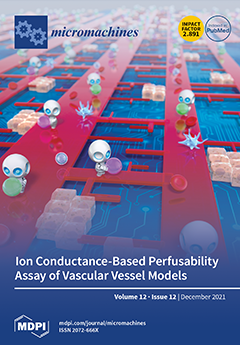
A novel methodology based on ion conductance has been presented to evaluate the perfusability of blood vessels constructed in microfluidic devices without microscopic imaging. A pair of electrodes were used to obtain ion currents through the mimicked vessels. The observed ion currents correlated with the perfusability of the vessel. Therefore, the methodology will be applied to drug screening using organs-on-a-chip including blood vessels. In the cover, “ion current flow” has been anthropomorphized as microrobots which bring ions in the blood vessel consisting of vascular endothelial cells. Electronic circuits have been drawn to represent the electrochemical analysis. The original design was created by the first author of this paper, Rise Akasaka, and the cover was completed by a scientific graphic designer.View this paper
  • Issues are regarded as officially published after their release is announced to the table of contents alert mailing list.
  • You may sign up for e-mail alerts to receive table of contents of newly released issues.
  • PDF is the official format for papers published in both, html and pdf forms. To view the papers in pdf format, click on the "PDF Full-text" link, and use the free Adobe Reader to open them.
Order results
Result details
Section
Select all
Export citation of selected articles as:
15 pages, 3474 KiB  
Article
Biomimetic Artificial Joints Based on Multi-Material Pneumatic Actuators Developed for Soft Robotic Finger Application
by Shumi Zhao, Yisong Lei, Ziwen Wang, Jie Zhang, Jianxun Liu, Pengfei Zheng, Zidan Gong and Yue Sun
Micromachines 2021, 12(12), 1593; https://doi.org/10.3390/mi12121593 - 20 Dec 2021
Cited by 5 | Viewed by 3099
Abstract
To precisely achieve a series of daily finger bending motions, a soft robotic finger corresponding to the anatomical range of each joint was designed in this study with multi-material pneumatic actuators. The actuator as a biomimetic artificial joint was developed on the basis [...] Read more.
To precisely achieve a series of daily finger bending motions, a soft robotic finger corresponding to the anatomical range of each joint was designed in this study with multi-material pneumatic actuators. The actuator as a biomimetic artificial joint was developed on the basis of two composite materials of different shear modules, and the pneumatic bellows as expansion parts was restricted by frame that made from polydimethylsiloxane (PDMS). A simplified mathematical model was used for the bending mechanism description and provides guidance for the multi-material pneumatic actuator fabrication (e.g., stiffness and thickness) and structural design (e.g., cross length and chamber radius), as well as the control parameter optimization (e.g., the air pressure supply). An actuation pressure of over 70 kPa is required by the developed soft robotic finger to provide a full motion range (MCP = 36°, PIP = 114°, and DIP = 75°) for finger action mimicking. In conclusion, a multi-material pneumatic actuator was designed and developed for soft robotic finger application and theoretically and experimentally demonstrated its feasibility in finger action mimicking. This study explored the mechanical properties of the actuator and could provide evidence-based technical parameters for pneumatic robotic finger design and precise control of its dynamic air pressure dosages in mimicking actions. Thereby, the conclusion was supported by the results theoretically and experimentally, which also aligns with our aim to design and develop a multi-material pneumatic actuator as a biomimetic artificial joint for soft robotic finger application. Full article
(This article belongs to the Special Issue Wearable Devices for Healthcare)
Show Figures

Figure 1

14 pages, 5035 KiB  
Article
Numerical Simulation of the Photobleaching Process in Laser-Induced Fluorescence Photobleaching Anemometer
by Yu Chen, Shuangshuang Meng, Kaige Wang, Jintao Bai and Wei Zhao
Micromachines 2021, 12(12), 1592; https://doi.org/10.3390/mi12121592 - 20 Dec 2021
Cited by 2 | Viewed by 2203
Abstract
At present, a novel flow diagnostic technique for micro/nanofluidics velocity measurement—laser-induced fluorescence photobleaching anemometer (LIFPA)—has been developed and successfully applied in broad areas, e.g., electrokinetic turbulence in micromixers and AC electroosmotic flow. Nevertheless, in previous investigations, to qualitatively reveal the dynamics of the [...] Read more.
At present, a novel flow diagnostic technique for micro/nanofluidics velocity measurement—laser-induced fluorescence photobleaching anemometer (LIFPA)—has been developed and successfully applied in broad areas, e.g., electrokinetic turbulence in micromixers and AC electroosmotic flow. Nevertheless, in previous investigations, to qualitatively reveal the dynamics of the photobleaching process of LIFPA, an approximation of uniform laser distribution was applied. This is different from the actual condition where the laser power density distribution is normally Gaussian. In this investigation, we numerically studied the photobleaching process of fluorescent dye in the laser focus region, according to the convection–diffusion reaction equation. The profiles of effective dye concentration and fluorescence were elucidated. The relationship between the commonly used photobleaching time constant obtained by experiments and the photochemical reaction coefficient is revealed. With the established model, we further discuss the effective spatial resolution of LIFPA and study the influence of the detection region of fluorescence on the performance of the LIFPA system. It is found that at sufficiently high excitation laser power density, LIFPA can even achieve a super-resolution that breaks the limit of optical diffraction. We hope the current investigation can reveal the photobleaching process of fluorescent dye under high laser power density illumination, to enhance our understanding of fluorescent dynamics and photochemistry and develop more powerful photobleaching-related flow diagnostic techniques. Full article
(This article belongs to the Special Issue MEMS and Microfluidic Devices for Analytical Chemistry and Biosensing)
Show Figures

Figure 1

10 pages, 3481 KiB  
Article
Study of Microscale Meniscus Confined Electrodeposition Based on COMSOL
by Fuyue Zhang, Dongjie Li, Weibin Rong, Liu Yang and Yu Zhang
Micromachines 2021, 12(12), 1591; https://doi.org/10.3390/mi12121591 - 20 Dec 2021
Cited by 9 | Viewed by 3208
Abstract
The rate and quality of microscale meniscus confined electrodeposition represent the key to micromanipulation based on electrochemistry and are extremely susceptible to the ambient relative humidity, electrolyte concentration, and applied voltage. To solve this problem, based on a neural network and genetic algorithm [...] Read more.
The rate and quality of microscale meniscus confined electrodeposition represent the key to micromanipulation based on electrochemistry and are extremely susceptible to the ambient relative humidity, electrolyte concentration, and applied voltage. To solve this problem, based on a neural network and genetic algorithm approach, this paper optimizes the process parameters of the microscale meniscus confined electrodeposition to achieve high-efficiency and -quality deposition. First, with the COMSOL Multiphysics, the influence factors of electrodeposition were analyzed and the range of high efficiency and quality electrodeposition parameters were discovered. Second, based on the back propagation (BP) neural network, the relationships between influence factors and the rate of microscale meniscus confined electrodeposition were established. Then, in order to achieve effective electrodeposition, the determined electrodeposition rate of 5 × 10⁻⁸ m/s was set as the target value, and the genetic algorithm was used to optimize each parameter. Finally, based on the optimization parameters obtained, we proceeded with simulations and experiments. The results indicate that the deposition rate maximum error is only 2.0% in experiments. The feasibility and accuracy of the method proposed in this paper were verified. Full article
Show Figures

Figure 1

14 pages, 5382 KiB  
Article
Using Modified-Intake Plasma-Enhanced Metal–Organic Chemical Vapor Deposition System to Grow Gallium Doped Zinc Oxide
by Po-Hsun Lei, Jia-Jan Chen, Ming-Hsiu Song, Yuan-Yu Zhan and Zong-Lin Jiang
Micromachines 2021, 12(12), 1590; https://doi.org/10.3390/mi12121590 - 20 Dec 2021
Cited by 2 | Viewed by 2204
Abstract
We have used a modified-intake plasma-enhanced metal–organic chemical vapor deposition (MIPEMOCVD) system to fabricate gallium-doped zinc oxide (GZO) thin films with varied Ga content. The MIPEMOCVD system contains a modified intake system of a mixed tank and a spraying terminal to deliver the [...] Read more.
We have used a modified-intake plasma-enhanced metal–organic chemical vapor deposition (MIPEMOCVD) system to fabricate gallium-doped zinc oxide (GZO) thin films with varied Ga content. The MIPEMOCVD system contains a modified intake system of a mixed tank and a spraying terminal to deliver the metal–organic (MO) precursors and a radio-frequency (RF) system parallel to the substrate normal, which can achieve a uniform distribution of organic precursors in the reaction chamber and reduce the bombardment damage. We examined the substitute and interstitial mechanisms of Ga atoms in zinc oxide (ZnO) matrix in MIPEMOCVD-grown GZO thin films through crystalline analyses and Hall measurements. The optimal Ga content of MIPEMOCVD-grown GZO thin film is 3.01 at%, which shows the highest conductivity and transmittance. Finally, the optimal MIPEMOCVD-grown GZO thin film was applied to n-ZnO/p-GaN LED as a window layer. As compared with the indium–tin–oxide (ITO) window layer, the n-ZnO/p-GaN LED with the MIPEMOCVD-grown GZO window layer of the rougher surface and higher transmittance at near UV range exhibits an enhanced light output power owing to the improved light extraction efficiency (LEE). Full article
Show Figures

Figure 1

16 pages, 2693 KiB  
Article
Numerical Study on Flow and Heat Transfer Characteristics of Trapezoidal Printed Circuit Heat Exchanger
by Yuxuan Ji, Kaixiang Xing, Kefa Cen, Mingjiang Ni, Haoran Xu and Gang Xiao
Micromachines 2021, 12(12), 1589; https://doi.org/10.3390/mi12121589 - 20 Dec 2021
Cited by 6 | Viewed by 2622
Abstract
Printed circuit heat exchanger (PCHE) is a promising regenerative device in the sCO2 power cycle, with the advantages of a large specific surface area and compact structure. Its tiny and complex flow channel structure brings enhanced heat transfer performance, while increasing pressure [...] Read more.
Printed circuit heat exchanger (PCHE) is a promising regenerative device in the sCO2 power cycle, with the advantages of a large specific surface area and compact structure. Its tiny and complex flow channel structure brings enhanced heat transfer performance, while increasing pressure drop losses. It is, thus, important to balance heat transfer and flow resistance performances with the consideration of sCO2 as the working agent. Herein, three-dimensional models are built with a full consideration of fluid flow and heat transfer fields. A trapezoidal channel is developed and its thermal–hydraulic performances are compared with the straight, the S-shape, and the zigzag structures. Nusselt numbers and the Fanning friction factors are analyzed with respect to the changes in Reynolds numbers and structure geometric parameters. A sandwiched structure that couples two hot channels with one cold channel is further designed to match the heat transfer capacity and the velocity of sCO2 flows between different sides. Through this novel design, we can reduce the pressure drop by 75% and increase the regenerative efficiency by 5%. This work can serve as a solid reference for the design and applications of PCHEs. Full article
(This article belongs to the Special Issue Feature Papers of Micromachines in Engineering and Technology 2021)
Show Figures

Graphical abstract

16 pages, 481 KiB  
Article
Evaluation of Self-Field Effects in Magnetometers Based on Meander-Shaped Arrays of Josephson Junctions or SQUIDs Connected in Series
by Denis Crété, Julien Kermorvant, Yves Lemaître, Bruno Marcilhac, Salvatore Mesoraca, Juan Trastoy and Christian Ulysse
Micromachines 2021, 12(12), 1588; https://doi.org/10.3390/mi12121588 - 20 Dec 2021
Cited by 3 | Viewed by 2365
Abstract
Arrays of superconducting quantum interference devices (SQUIDs) are highly sensitive magnetometers that can operate without a flux-locked loop, as opposed to single SQUID magnetometers. They have no source of ambiguity and benefit from a larger bandwidth. They can be used to measure absolute [...] Read more.
Arrays of superconducting quantum interference devices (SQUIDs) are highly sensitive magnetometers that can operate without a flux-locked loop, as opposed to single SQUID magnetometers. They have no source of ambiguity and benefit from a larger bandwidth. They can be used to measure absolute magnetic fields with a dynamic range scaling as the number of SQUIDs they contain. A very common arrangement for a series array of SQUIDs is with meanders as it uses the substrate area efficiently. As for most layouts with long arrays, this layout breaks the symmetry required for the elimination of adverse self-field effects. We investigate the scaling behavior of series arrays of SQUIDs, taking into account the self-field generated by the bias current flowing along the meander. We propose a design for the partial compensation of this self-field. In addition, we provide a comparison with the case of series arrays of long Josephson junctions, using the Fraunhofer pattern for applications in magnetometry. We find that compensation is required for arrays of the larger size and that, depending on the technology, arrays of long Josephson junctions may have better performance than arrays of SQUIDs. Full article
(This article belongs to the Special Issue Nano and Micro Superconducting Quantum Interference Devices)
Show Figures

Figure 1

16 pages, 43467 KiB  
Article
Design and Implementation of a Flexible Photovoltaic Emulator Using a GaN-Based Synchronous Buck Converter
by Chao-Tsung Ma, Zhen-Yu Tsai, Hung-Hsien Ku and Chin-Lung Hsieh
Micromachines 2021, 12(12), 1587; https://doi.org/10.3390/mi12121587 - 20 Dec 2021
Cited by 4 | Viewed by 2302
Abstract
In order to efficiently facilitate various research works related to power converter design and testing for solar photovoltaic (PV) generation systems, it is a great merit to use advanced power-converter-based and digitally controlled PV emulators in place of actual PV modules to reduce [...] Read more.
In order to efficiently facilitate various research works related to power converter design and testing for solar photovoltaic (PV) generation systems, it is a great merit to use advanced power-converter-based and digitally controlled PV emulators in place of actual PV modules to reduce the space, cost, and time to obtain the required scenarios of solar irradiances for various functional tests. This paper presents a flexible PV emulator based on gallium nitride (GaN), a wide-bandgap (WBG) semiconductor, and a based synchronous buck converter and controlled with a digital signal processor (DSP). With the help of GaN-based switching devices, the proposed emulator can accurately mimic the dynamic voltage-current characteristics of any PV module under normal irradiance and partial shading conditions. With the proposed PV emulator, it is possible to closely emulate any PV module characteristic both theoretically, based on manufacturer’s datasheets, and experimentally, based on measured data from practical PV modules. A curve fitting algorithm is used to handle the real-time generation of control signals for the digital controller. Both simulation with computer software and implementation on 1 kW GaN-based experimental hardware using Texas Instruments DSP as the controller have been carried out. Results show that the proposed emulator achieves efficiency as high as 99.05% and exhibits multifaceted application features in tracking various PV voltage and current parameters, demonstrating the feasibility and excellent performance of the proposed PV emulator. Full article
Show Figures

Figure 1

12 pages, 3332 KiB  
Communication
Wafer-Level 3D Integration Based on Poly (Diallyl Phthalate) Adhesive Bonding
by Zhong Fang, Peng You, Yijie Jia, Xuchao Pan, Yunlei Shi, Junjie Jiao and Yong He
Micromachines 2021, 12(12), 1586; https://doi.org/10.3390/mi12121586 - 20 Dec 2021
Cited by 1 | Viewed by 2447
Abstract
Three-dimensional integration technology provides a promising total solution that can be used to achieve system-level integration with high function density and low cost. In this study, a wafer-level 3D integration technology using PDAP as an intermediate bonding polymer was applied effectively for integration [...] Read more.
Three-dimensional integration technology provides a promising total solution that can be used to achieve system-level integration with high function density and low cost. In this study, a wafer-level 3D integration technology using PDAP as an intermediate bonding polymer was applied effectively for integration with an SOI wafer and dummy a CMOS wafer. The influences of the procedure parameters on the adhesive bonding effects were determined by Si–Glass adhesive bonding tests. It was found that the bonding pressure, pre-curing conditions, spin coating conditions, and cleanliness have a significant influence on the bonding results. The optimal procedure parameters for PDAP adhesive bonding were obtained through analysis and comparison. The 3D integration tests were conducted according to these optimal parameters. In the tests, process optimization was focused on Si handle-layer etching, PDAP layer etching, and Au pillar electroplating. After that, the optimal process conditions for the 3D integration process were achieved. The 3D integration applications of the micro-bolometer array and the micro-bridge resistor array were presented. It was confirmed that 3D integration based on PDAP adhesive bonding is suitable for the fabrication of system-on-chip when using MEMS and IC integration and that it is especially useful for the fabrication of low-cost suspended-microstructure on-CMOS-chip systems. Full article
(This article belongs to the Special Issue Micro- and Nano-Systems for Manipulation, Actuation and Sensing)
Show Figures

Figure 1

11 pages, 3411 KiB  
Article
Detection of Senecionine in Dietary Sources by Single-Use Electrochemical Sensor
by Huseyin Senturk, Ece Eksin, Ulvi Zeybek and Arzum Erdem
Micromachines 2021, 12(12), 1585; https://doi.org/10.3390/mi12121585 - 20 Dec 2021
Cited by 8 | Viewed by 2583
Abstract
Pyrrolizidine alkaloids (PAs) are produced by plants as secondary compounds that are the most widely distributed natural toxins. There have been many cases of human toxicity caused by consumption of toxic plant species, as herbal teas and grain or grain products contaminated with [...] Read more.
Pyrrolizidine alkaloids (PAs) are produced by plants as secondary compounds that are the most widely distributed natural toxins. There have been many cases of human toxicity caused by consumption of toxic plant species, as herbal teas and grain or grain products contaminated with PA-containing seeds have been reported. Companies that produce dried spices and tea leaves should examine the PA level in their products. For the first time in the literature, a simple and inexpensive electrochemical assay based on a single-use sensor was introduced for quantitative determination of senecionine (SEN) in the most frequently contaminated food sources. SEN was immobilized on a pencil graphite electrode surface by the passive adsorption technique. Differential pulse voltammetry (DPV) was used to evaluate the oxidation signal of SEN, which was observed to be around +0.95 V. The oxidation signal was specific to the SEN in the sample, and the current value was proportional to its concentration. The selectivity of our assay was also tested in the presence of other similar PAs such as intermedine, lycopsamine, and heliotrine. The detection limit is calculated by developed assay and found to be 5.45 µg/mL, which is an acceptable concentration value of SEN occurring at toxic levels for consumers. As an application of the developed sensor in food products, the electrochemical detection of SEN was successfully performed in flour and herbal tea products. Full article
(This article belongs to the Special Issue Nanomaterials Modified Electrochemical Sensors)
Show Figures

Graphical abstract

18 pages, 7100 KiB  
Review
Metasurface Photodetectors
by Jinzhao Li, Junyu Li, Shudao Zhou and Fei Yi
Micromachines 2021, 12(12), 1584; https://doi.org/10.3390/mi12121584 - 20 Dec 2021
Cited by 13 | Viewed by 5594
Abstract
Photodetectors are the essential building blocks of a wide range of optical systems. Typical photodetectors only convert the intensity of light electrical output signals, leaving other electromagnetic parameters, such as the frequencies, phases, and polarization states unresolved. Metasurfaces are arrays of subwavelength structures [...] Read more.
Photodetectors are the essential building blocks of a wide range of optical systems. Typical photodetectors only convert the intensity of light electrical output signals, leaving other electromagnetic parameters, such as the frequencies, phases, and polarization states unresolved. Metasurfaces are arrays of subwavelength structures that can manipulate the amplitude, phase, frequency, and polarization state of light. When combined with photodetectors, metasurfaces can enhance the light-matter interaction at the pixel level and also enable the detector pixels to resolve more electromagnetic parameters. In this paper, we review recent research efforts in merging metasurfaces with photodetectors towards improved detection performances and advanced detection schemes. The impacts of merging metasurfaces with photodetectors, on the architecture of optical systems, and potential applications are also discussed. Full article
(This article belongs to the Special Issue 2D Materials Optoelectronic and Nanophotonic Devices)
Show Figures

Figure 1

15 pages, 2538 KiB  
Article
Static and Dynamic Optical Analysis of Micro Wrinkle Formation on a Liquid Surface
by Antariksh Saxena, Costas Tsakonas, David Chappell, Chi Shing Cheung, Andrew Michael John Edwards, Haida Liang, Ian Charles Sage and Carl Vernon Brown
Micromachines 2021, 12(12), 1583; https://doi.org/10.3390/mi12121583 - 19 Dec 2021
Cited by 1 | Viewed by 2221
Abstract
A spatially periodic voltage was used to create a dielectrophoresis induced periodic micro wrinkle deformation on the surface of a liquid film. Optical Coherence Tomography provided the equilibrium wrinkle profile at submicron accuracy. The dynamic wrinkle amplitude was derived from optical diffraction analysis [...] Read more.
A spatially periodic voltage was used to create a dielectrophoresis induced periodic micro wrinkle deformation on the surface of a liquid film. Optical Coherence Tomography provided the equilibrium wrinkle profile at submicron accuracy. The dynamic wrinkle amplitude was derived from optical diffraction analysis during sub-millisecond wrinkle formation and decay, after abruptly increasing or reducing the voltage, respectively. The decay time constant closely followed the film thickness dependence expected for surface tension driven viscous levelling. Modelling of the system using numerical solution of the Stokes flow equations with electrostatic forcing predicted that wrinkle formation was faster than decay, in accord with observations. Full article
(This article belongs to the Special Issue Advances in Electrowetting Devices)
Show Figures

Figure 1

12 pages, 3908 KiB  
Article
Microfluidic Chip with Two-Stage Isothermal Amplification Method for Highly Sensitive Parallel Detection of SARS-CoV-2 and Measles Virus
by Qin Huang, Xiaohui Shan, Ranran Cao, Xiangyu Jin, Xue Lin, Qiurong He, Yulei Zhu, Rongxin Fu, Wenli Du, Wenqi Lv, Ying Xia and Guoliang Huang
Micromachines 2021, 12(12), 1582; https://doi.org/10.3390/mi12121582 - 19 Dec 2021
Cited by 16 | Viewed by 2964
Abstract
A two-stage isothermal amplification method, which consists of a first-stage basic recombinase polymerase amplification (RPA) and a second-stage fluorescence loop-mediated isothermal amplification (LAMP), as well as a microfluidic-chip-based portable system, were developed in this study; these enabled parallel detection of multiplex targets in [...] Read more.
A two-stage isothermal amplification method, which consists of a first-stage basic recombinase polymerase amplification (RPA) and a second-stage fluorescence loop-mediated isothermal amplification (LAMP), as well as a microfluidic-chip-based portable system, were developed in this study; these enabled parallel detection of multiplex targets in real time in around one hour, with high sensitivity and specificity, without cross-contamination. The consumption of the sample and the reagent was 2.1 μL and 10.6 μL per reaction for RPA and LAMP, respectively. The lowest detection limit (LOD) was about 10 copies. The clinical amplification of about 40 nasopharyngeal swab samples, containing 17 SARS-CoV-2 (severe acute respiratory syndrome coronavirus) and 23 measles viruses (MV), were parallel tested by using the microfluidic chip. Both clinical specificity and sensitivity were 100% for MV, and the clinical specificity and sensitivity were 94.12% and 95.83% for SARS-CoV-2, respectively. This two-stage isothermal amplification method based on the microfluidic chip format offers a convenient, clinically parallel molecular diagnostic method, which can identify different nucleic acid samples simultaneously and in a timely manner, and with a low cost of the reaction reagent. It is especially suitable for resource-limited areas and point-of-care testing (POCT). Full article
(This article belongs to the Special Issue MEMS and Microfluidic Devices for Analytical Chemistry and Biosensing)
Show Figures

Figure 1

14 pages, 1886 KiB  
Article
Nanoribbon Biosensor in the Detection of miRNAs Associated with Colorectal Cancer
by Yuri D. Ivanov, Kristina V. Goldaeva, Kristina A. Malsagova, Tatyana O. Pleshakova, Rafael A. Galiullin, Vladimir P. Popov, Nikolay E. Kushlinskii, Alexander A. Alferov, Dmitry V. Enikeev, Natalia V. Potoldykova and Alexander I. Archakov
Micromachines 2021, 12(12), 1581; https://doi.org/10.3390/mi12121581 - 18 Dec 2021
Cited by 5 | Viewed by 2630
Abstract
A nanoribbon biosensor (NRBS) was developed to register synthetic DNAs that simulate and are analogous to miRNA-17-3p associated with colorectal cancer. Using this nanoribbon biosensor, the ability to detect miRNA-17-3p in the blood plasma of a patient diagnosed with colorectal cancer has been [...] Read more.
A nanoribbon biosensor (NRBS) was developed to register synthetic DNAs that simulate and are analogous to miRNA-17-3p associated with colorectal cancer. Using this nanoribbon biosensor, the ability to detect miRNA-17-3p in the blood plasma of a patient diagnosed with colorectal cancer has been demonstrated. The sensing element of the NRBS was a nanochip based on a silicon-on-insulator (SOI) nanostructure. The nanochip included an array of 10 nanoribbons and was designed with the implementation of top-down technology. For biospecific recognition of miRNA-17-3p, the nanochip was modified with DNA probes specific for miRNA-17-3p. The performance of the nanochip was preliminarily tested on model DNA oligonucleotides, which are synthetic analogues of miRNA-17-3p, and a detection limit of ~10−17 M was achieved. The results of this work can be used in the development of serological diagnostic systems for early detection of colorectal cancer. Full article
(This article belongs to the Special Issue Advances in Biomedical Nanotechnology)
Show Figures

Figure 1

13 pages, 4736 KiB  
Article
Analysis of Aspect Ratio in a Miniature Rectangle Channel for Low Frictional Resistance
by Takashi Fukuda and Makoto Ryo Harada
Micromachines 2021, 12(12), 1580; https://doi.org/10.3390/mi12121580 - 18 Dec 2021
Viewed by 1927
Abstract
We conducted a theoretical investigation of the cross-sectional aspect ratio of a rectangular channel to have sufficiently low frictional resistance under less than 150 of the Reynolds number. From the theoretical consideration, it was clarified that 3.40 or more is recommended as a [...] Read more.
We conducted a theoretical investigation of the cross-sectional aspect ratio of a rectangular channel to have sufficiently low frictional resistance under less than 150 of the Reynolds number. From the theoretical consideration, it was clarified that 3.40 or more is recommended as a criterion for determining the aspect ratio. This addresses the problem of determining the interval of rectangle channels, installed in a plate reactor. There is a concern that the real system does not follow the analytical solution, assuming laminar flow, since the higher aspect ratio leads to disturbances of the flow such as the emergence of vortices. However, in the channel’s volume range of (W × H × L) = (7.0 mm × 0.38 mm × 0.26 m), such a turbulence was not observed in the detailed numerical calculation by CFD, where both calculation results were in agreement to within 3% accuracy. Moreover, even in an experimental system with a surface roughness of ca. 7%, friction resistance took agreement within an accuracy of ±30%. Full article
(This article belongs to the Section E:Engineering and Technology)
Show Figures

Figure 1

11 pages, 3246 KiB  
Article
Index Modulation Embedded in Type I Waveguide Written by Femtosecond Laser in Fused Silica
by Jing Lv, Razvan Stoian, Guanghua Cheng and Kedian Wang
Micromachines 2021, 12(12), 1579; https://doi.org/10.3390/mi12121579 - 18 Dec 2021
Cited by 2 | Viewed by 2771
Abstract
Slit-shaped laser beams focused in bulk optical materials can realize embedded waveguides with circular cross sections consisting of positive index change type I traces. In these kinds of waveguide traces, a peculiar periodical refractive index modulation was observed in type I waveguides with [...] Read more.
Slit-shaped laser beams focused in bulk optical materials can realize embedded waveguides with circular cross sections consisting of positive index change type I traces. In these kinds of waveguide traces, a peculiar periodical refractive index modulation was observed in type I waveguides with two different femtosecond lasers. The direction of refractive index modulation can be controlled with the slit configuration, and its period can be controlled by mechanical perturbation of the stages and the scanning speed. We argue that platform perturbation and dynamical thermal transport processes during the scan are generating factors in the appearance of this modulation. The embedded microstructures in waveguides can provide spectrum modulation, which may have potential applications in optical sensing, filtering, and phase control. Full article
Show Figures

Figure 1

14 pages, 7221 KiB  
Article
Individual Microparticle Manipulation Using Combined Electroosmosis and Dielectrophoresis through a Si3N4 Film with a Single Micropore
by Chenang Lyu, Leo Lou, Matthew J. Powell-Palm, Gideon Ukpai, Xing Li and Boris Rubinsky
Micromachines 2021, 12(12), 1578; https://doi.org/10.3390/mi12121578 - 18 Dec 2021
Viewed by 1875
Abstract
Porous dielectric membranes that perform insulator-based dielectrophoresis or electroosmotic pumping are commonly used in microchip technologies. However, there are few fundamental studies on the electrokinetic flow patterns of single microparticles around a single micropore in a thin dielectric film. Such a study would [...] Read more.
Porous dielectric membranes that perform insulator-based dielectrophoresis or electroosmotic pumping are commonly used in microchip technologies. However, there are few fundamental studies on the electrokinetic flow patterns of single microparticles around a single micropore in a thin dielectric film. Such a study would provide fundamental insights into the electrokinetic phenomena around a micropore, with practical applications regarding the manipulation of single cells and microparticles by focused electric fields. We have fabricated a device around a silicon nitride film with a single micropore (2–4 µm in diameter) which has the ability to locally focus electric fields on the micropore. Single microscale polystyrene beads were used to study the electrokinetic flow patterns. A mathematical model was developed to support the experimental study and evaluate the electric field distribution, fluid motion, and bead trajectories. Good agreement was found between the mathematic model and the experimental data. We show that the combination of electroosmotic flow and dielectrophoretic force induced by direct current through a single micropore can be used to trap, agglomerate, and repel microparticles around a single micropore without an external pump. The scale of our system is practically relevant for the manipulation of single mammalian cells, and we anticipate that our single-micropore approach will be directly employable in applications ranging from fundamental single cell analyses to high-precision single cell electroporation or cell fusion. Full article
(This article belongs to the Special Issue Micro/Nanofluidic Devices for Single Cell Analysis, Volume III)
Show Figures

Figure 1

13 pages, 5024 KiB  
Article
Theoretical and Experimental Investigations into a Crawling Robot Propelled by Piezoelectric Material
by Xiangli Zeng, Yue Wu, Shangyan Han, Yanbo Liu, Haohua Xiu, Fengjun Tian and Luquan Ren
Micromachines 2021, 12(12), 1577; https://doi.org/10.3390/mi12121577 - 18 Dec 2021
Cited by 4 | Viewed by 2164
Abstract
Conventional motors with complicated electromagnetic structures are difficult to miniaturise for millimetre- and centimetre-sized robots. Instead, small-scale robots are actuated using a variety of functional materials. We proposed a novel robot propelled by a piezoelectric ceramic in this work. The robot advances due [...] Read more.
Conventional motors with complicated electromagnetic structures are difficult to miniaturise for millimetre- and centimetre-sized robots. Instead, small-scale robots are actuated using a variety of functional materials. We proposed a novel robot propelled by a piezoelectric ceramic in this work. The robot advances due to the asymmetric friction created by the spikes on the surface. The structural modelling was completed, static and dynamic models were established to predict the moving characteristics, the prototype was built using three dimensional (3D) printing technology, and the models were evaluated via experiments. Compared with conventional inchworm-type robots, the proposed robot is superior in simple structure because the clamping components are replaced by spikes with asymmetric friction. Compared with SMA (shape memory alloy) actuating inchworm-type robots, it has a faster velocity with higher resolution. Meanwhile, the components are printed through an additive manufacturing process that is convenient and avoids assembly errors. This design could make contributions to many areas, such as pipe inspection, earthquake rescue, and medicine delivery. Full article
Show Figures

Figure 1

10 pages, 2461 KiB  
Article
Ionic-Liquid Gating in Two-Dimensional TMDs: The Operation Principles and Spectroscopic Capabilities
by Daniel Vaquero, Vito Clericò, Juan Salvador-Sánchez, Jorge Quereda, Enrique Diez and Ana M. Pérez-Muñoz
Micromachines 2021, 12(12), 1576; https://doi.org/10.3390/mi12121576 - 17 Dec 2021
Cited by 6 | Viewed by 3606
Abstract
Ionic-liquid gating (ILG) is able to enhance carrier densities well above the achievable values in traditional field-effect transistors (FETs), revealing it to be a promising technique for exploring the electronic phases of materials in extreme doping regimes. Due to their chemical stability, transition [...] Read more.
Ionic-liquid gating (ILG) is able to enhance carrier densities well above the achievable values in traditional field-effect transistors (FETs), revealing it to be a promising technique for exploring the electronic phases of materials in extreme doping regimes. Due to their chemical stability, transition metal dichalcogenides (TMDs) are ideal candidates to produce ionic-liquid-gated FETs. Furthermore, as recently discovered, ILG can be used to obtain the band gap of two-dimensional semiconductors directly from the simple transfer characteristics. In this work, we present an overview of the operation principles of ionic liquid gating in TMD-based transistors, establishing the importance of the reference voltage to obtain hysteresis-free transfer characteristics, and hence, precisely determine the band gap. We produced ILG-based bilayer WSe2 FETs and demonstrated their ambipolar behavior. We estimated the band gap directly from the transfer characteristics, demonstrating the potential of ILG as a spectroscopy technique. Full article
Show Figures

Figure 1

11 pages, 5165 KiB  
Article
Low Temperature Hydrophilic SiC Wafer Level Direct Bonding for Ultrahigh-Voltage Device Applications
by Wenting Zhang, Caorui Zhang, Junmin Wu, Fei Yang, Yunlai An, Fangjing Hu and Ji Fan
Micromachines 2021, 12(12), 1575; https://doi.org/10.3390/mi12121575 - 17 Dec 2021
Cited by 3 | Viewed by 2688
Abstract
SiC direct bonding using O2 plasma activation is investigated in this work. SiC substrate and n SiC epitaxy growth layer are activated with an optimized duration of 60s and power of the oxygen ion beam source at 20 W. After O [...] Read more.
SiC direct bonding using O2 plasma activation is investigated in this work. SiC substrate and n SiC epitaxy growth layer are activated with an optimized duration of 60s and power of the oxygen ion beam source at 20 W. After O2 plasma activation, both the SiC substrate and n SiC epitaxy growth layer present a sufficient hydrophilic surface for bonding. The two 4-inch wafers are prebonded at room temperature followed by an annealing process in an atmospheric N2 ambient for 3 h at 300 °C. The scanning results obtained by C-mode scanning acoustic microscopy (C-SAM) shows a high bonding uniformity. The bonding strength of 1473 mJ/m2 is achieved. The bonding mechanisms are investigated through interface analysis by transmission electron microscopy (TEM) and energy dispersive X-ray spectroscopy (EDX). Oxygen is found between the two interfaces, which indicates Si–O and C–O are formed at the bonding interface. However, a C-rich area is also detected at the bonding interface, which reveals the formation of C-C bonds in the activated SiC surface layer. These results show the potential of low cost and efficient surface activation method for SiC direct bonding for ultrahigh-voltage devices applications. Full article
(This article belongs to the Special Issue Two-Dimensional Materials for Advanced Electronic Devices)
Show Figures

Figure 1

15 pages, 3541 KiB  
Article
A Cerebral Organoid Connectivity Apparatus to Model Neuronal Tract Circuitry
by Denise A. Robles, Andrew J. Boreland, Zhiping P. Pang and Jeffrey D. Zahn
Micromachines 2021, 12(12), 1574; https://doi.org/10.3390/mi12121574 - 17 Dec 2021
Cited by 4 | Viewed by 3157
Abstract
Mental disorders have high prevalence, but the efficacy of existing therapeutics is limited, in part, because the pathogenic mechanisms remain enigmatic. Current models of neural circuitry include animal models and post-mortem brain tissue, which have allowed enormous progress in understanding the pathophysiology of [...] Read more.
Mental disorders have high prevalence, but the efficacy of existing therapeutics is limited, in part, because the pathogenic mechanisms remain enigmatic. Current models of neural circuitry include animal models and post-mortem brain tissue, which have allowed enormous progress in understanding the pathophysiology of mental disorders. However, these models limit the ability to assess the functional alterations in short-range and long-range network connectivity between brain regions that are implicated in many mental disorders, e.g., schizophrenia and autism spectrum disorders. This work addresses these limitations by developing an in vitro model of the human brain that models the in vivo cerebral tract environment. In this study, microfabrication and stem cell differentiation techniques were combined to develop an in vitro cerebral tract model that anchors human induced pluripotent stem cell-derived cerebral organoids (COs) and provides a scaffold to promote the formation of a functional connecting neuronal tract. Two designs of a Cerebral Organoid Connectivity Apparatus (COCA) were fabricated using SU-8 photoresist. The first design contains a series of spikes which anchor the CO to the COCA (spiked design), whereas the second design contains flat supporting structures with open holes in a grid pattern to anchor the organoids (grid design); both designs allow effective media exchange. Morphological and functional analyses reveal the expression of key neuronal markers as well as functional activity and signal propagation along cerebral tracts connecting CO pairs. The reported in vitro models enable the investigation of critical neural circuitry involved in neurodevelopmental processes and has the potential to help devise personalized and targeted therapeutic strategies. Full article
(This article belongs to the Special Issue Microfluidic Platforms for the Nervous System)
Show Figures

Figure 1

2 pages, 160 KiB  
Editorial
Micromachines: 5000th Publications Milestone
by Nam-Trung Nguyen
Micromachines 2021, 12(12), 1573; https://doi.org/10.3390/mi12121573 - 17 Dec 2021
Viewed by 1360
Abstract
Micromachines has achieved a major milestone this year [...] Full article
14 pages, 5788 KiB  
Article
Development of Cell-Carrying Magnetic Microrobots with Bioactive Nanostructured Titanate Surface for Enhanced Cell Adhesion
by Junyang Li, Lei Fan, Yanfang Li, Tanyong Wei, Cheng Wang, Feng Li, Hua Tian and Dong Sun
Micromachines 2021, 12(12), 1572; https://doi.org/10.3390/mi12121572 - 17 Dec 2021
Cited by 4 | Viewed by 2714
Abstract
Cell-carrying magnet-driven microrobots are easily affected by blood flow or body fluids during transportation in the body, and thus cells often fall off from the microrobots. To reduce the loss of loaded cells, we developed a microrobot with a bioactive nanostructured titanate surface [...] Read more.
Cell-carrying magnet-driven microrobots are easily affected by blood flow or body fluids during transportation in the body, and thus cells often fall off from the microrobots. To reduce the loss of loaded cells, we developed a microrobot with a bioactive nanostructured titanate surface (NTS), which enhances cell adhesion. The microrobot was fabricated using 3D laser lithography and coated with nickel for magnetic actuation. Then, the microrobot was coated with titanium for the external generation of an NTS through reactions in NaOH solution. Enhanced cell adhesion may be attributed to the changes in the surface wettability of the microrobot and in the morphology of the loaded cells. An experiment was performed on a microfluidic chip for the simulation of blood flow environment, and result revealed that the cells adhered closely to the microrobot with NTS and were not obviously affected by flow. The cell viability and protein absorption test and alkaline phosphatase activity assay indicated that NTS can provide a regulatory means for improving cell proliferation and early osteogenic differentiation. This research provided a novel microrobotic platform that can positively influence the behaviour of cells loaded on microrobots through surface nanotopography, thereby opening up a new route for microrobot cell delivery. Full article
(This article belongs to the Special Issue Micro- and Nano-Systems for Manipulation, Actuation and Sensing)
Show Figures

Figure 1

12 pages, 10572 KiB  
Article
Multiphoton Absorption Simulation of Sapphire Substrate under the Action of Femtosecond Laser for Larger Density of Pattern-Related Process Windows
by Xintian Cai, Chaoyue Ji, Changkai Li, Zhiqiang Tian, Xuan Wang, Cheng Lei and Sheng Liu
Micromachines 2021, 12(12), 1571; https://doi.org/10.3390/mi12121571 - 17 Dec 2021
Cited by 8 | Viewed by 2268
Abstract
It is essential to develop pattern-related process windows on substrate surface for reducing the dislocation density of wide bandgap semiconductor film growth. For extremely high instantaneous intensity and excellent photon absorption rate, femtosecond lasers are currently being increasingly adopted. However, the mechanism of [...] Read more.
It is essential to develop pattern-related process windows on substrate surface for reducing the dislocation density of wide bandgap semiconductor film growth. For extremely high instantaneous intensity and excellent photon absorption rate, femtosecond lasers are currently being increasingly adopted. However, the mechanism of the femtosecond laser developing pattern-related process windows on the substrate remains to be further revealed. In this paper, a model is established based on the Fokker–Planck equation and the two-temperature model (TTM) equation to simulate the ablation of a sapphire substrate under the action of a femtosecond laser. The transient nonlinear evolutions such as free electron density, absorption coefficient, and electron–lattice temperature are obtained. This paper focuses on simulating the multiphoton absorption of sapphire under femtosecond lasers of different wavelengths. The results show that within the range of 400 to 1030 nm, when the wavelength is large, the number of multiphoton required for ionization is larger, and wider and shallower ablation pits can be obtained. When the wavelength is smaller, the number of multiphoton is smaller, narrower and deeper ablation pits can be obtained. Under the simulation conditions presented in this paper, the minimum ablation pit depth can reach 0.11 μm and the minimum radius can reach 0.6 μm. In the range of 400 to 1030 nm, selecting a laser with a shorter wavelength can achieve pattern-related process windows with a smaller diameter, which is beneficial to increase the density of pattern-related process windows on the substrate surface. The simulation is consistent with existing theories and experimental results, and further reveals the transient nonlinear mechanism of the femtosecond laser developing the pattern-related process windows on the sapphire substrate. Full article
(This article belongs to the Topic Frontiers of Optomechanics of Nanocrystals)
Show Figures

Figure 1

3 pages, 195 KiB  
Editorial
Special Issue on Networks-on-Chip Again on the Rise: From Emerging Applications to Emerging Technologies
by Davide Bertozzi, José L. Abellán and Mahdi Nikdast
Micromachines 2021, 12(12), 1570; https://doi.org/10.3390/mi12121570 - 17 Dec 2021
Viewed by 1665
Abstract
Twenty years after the advent of interconnection networks to tackle the on-chip communication bottleneck [...] Full article
15 pages, 2299 KiB  
Article
Modeling the Double Layer Capacitance Effect in Electrolyte Gated FETs with Gel and Aqueous Electrolytes
by Roslyn S. Massey and Ravi Prakash
Micromachines 2021, 12(12), 1569; https://doi.org/10.3390/mi12121569 - 17 Dec 2021
Cited by 4 | Viewed by 2443
Abstract
Potential implementation of bio-gel Electrolyte Double Layer capacitors (bio-gel EDLCs) and electrolyte-gated FET biosensors, two commonly reported configurations of bio-electrolytic electronic devices, requires a robust analysis of their complex internal capacitive behavior. Presently there is neither enough of the parameter extraction literature, nor [...] Read more.
Potential implementation of bio-gel Electrolyte Double Layer capacitors (bio-gel EDLCs) and electrolyte-gated FET biosensors, two commonly reported configurations of bio-electrolytic electronic devices, requires a robust analysis of their complex internal capacitive behavior. Presently there is neither enough of the parameter extraction literature, nor an effective simulation model to represent the transient behavior of these systems. Our work aims to supplement present transient thin film transistor modelling techniques with the reported parameter extraction method, to accurately model both bio-gel EDLC and the aqueous electrolyte gated FET devices. Our parameter extraction method was tested with capacitors analogous to polymer-electrolyte gated FETs, electrolyte gated Field effect transistor (EGOFET) and Organic Electrolyte Gated Field Effect Transistor (OEGFET) capacitance stacks. Our method predicts the input/output electrical behavior of bio-gel EDLC and EGOFET devices far more accurately than conventional DLC techniques, with less than 5% error. It is also more effective in capturing the characteristic aqueous electrolyte charging behavior and maximum charging capability which are unique to these systems, than the conventional DLC Zubieta and the Two branch models. We believe this significant improvement in device simulation is a pivotal step towards further integration and commercial implementation of organic bio-electrolyte devices. The effective reproduction of the transient response of the OEGFET equivalent system also predicts the transient capacitive effects observed in our previously reported label-free OEGFET biosensor devices. This is the first parameter extraction method specifically designed for electrical parameter-based modelling of organic bio-electrolytic capacitor devices. Full article
Show Figures

Figure 1

3 pages, 175 KiB  
Editorial
Editorial for the Special Issue on Flash Memory Devices
by Cristian Zambelli and Rino Micheloni
Micromachines 2021, 12(12), 1566; https://doi.org/10.3390/mi12121566 - 17 Dec 2021
Viewed by 1943
Abstract
Flash memory devices represented a breakthrough in the storage industry since their inception in the mid-1980s, and innovation is still ongoing after more than 35 years [...] Full article
(This article belongs to the Special Issue Flash Memory Devices)
18 pages, 24835 KiB  
Article
A Prognostics Method Based on Back Propagation Neural Network for Corroded Pipelines
by Mingjiang Xie, Zishuo Li, Jianli Zhao and Xianjun Pei
Micromachines 2021, 12(12), 1568; https://doi.org/10.3390/mi12121568 - 16 Dec 2021
Cited by 7 | Viewed by 2175
Abstract
A method that employs the back propagation (BP) neural network is used to predict the growth of corrosion defect in pipelines. This method considers more diversified parameters that affect the pipeline’s corrosion rate, including pipe parameters, service life, corrosion type, corrosion location, corrosion [...] Read more.
A method that employs the back propagation (BP) neural network is used to predict the growth of corrosion defect in pipelines. This method considers more diversified parameters that affect the pipeline’s corrosion rate, including pipe parameters, service life, corrosion type, corrosion location, corrosion direction, and corrosion amount in a three-dimensional direction. The initial corrosion time is also considered, and, on this basis, the uncertainties of the initial corrosion time and the corrosion size are added to the BP neural network model. In this paper, three kinds of pipeline corrosion growth models are constructed: the traditional corrosion model, the corrosion model considering the uncertainties of initial corrosion time and corrosion depth, and corrosion model also considering the uncertainties of corrosion size (length, width, depth). The rationality and effectiveness of the proposed prediction models are verified by three case studies: the uniform model, the exponential model, and the gamma process model. The proposed models can be widely used in the prediction and management of pipeline corrosion. Full article
(This article belongs to the Special Issue Advanced Manufacturing Technology and Systems)
Show Figures

Figure 1

12 pages, 3576 KiB  
Article
Contact Engineering Approach to Improve the Linearity of Multilevel Memristive Devices
by Natalia Andreeva, Dmitriy Mazing, Alexander Romanov, Marina Gerasimova, Dmitriy Chigirev and Victor Luchinin
Micromachines 2021, 12(12), 1567; https://doi.org/10.3390/mi12121567 - 16 Dec 2021
Cited by 4 | Viewed by 1787
Abstract
Physical mechanisms underlying the multilevel resistive tuning over seven orders of magnitude in structures based on TiO2/Al2O3 bilayers, sandwiched between platinum electrodes, are responsible for the nonlinear dependence of the conductivity of intermediate resistance states on the writing [...] Read more.
Physical mechanisms underlying the multilevel resistive tuning over seven orders of magnitude in structures based on TiO2/Al2O3 bilayers, sandwiched between platinum electrodes, are responsible for the nonlinear dependence of the conductivity of intermediate resistance states on the writing voltage. To improve the linearity of the electric-field resistance tuning, we apply a contact engineering approach. For this purpose, platinum top electrodes were replaced with aluminum and copper ones to induce the oxygen-related electrochemical reactions at the interface with the Al2O3 switching layer of the structures. Based on experimental results, it was found that electrode material substitution provokes modification of the physical mechanism behind the resistive switching in TiO2/Al2O3 bilayers. In the case of aluminum electrodes, a memory window has been narrowed down to three orders of magnitude, while the linearity of resistance tuning was improved. For copper electrodes, a combination of effects related to metal ion diffusion with oxygen vacancies driven resistive switching was responsible for a rapid relaxation of intermediate resistance states in TiO2/Al2O3 bilayers. Full article
Show Figures

Figure 1

19 pages, 6336 KiB  
Article
Waveguide Manufacturing Technologies for Next-Generation Millimeter-Wave Antennas
by Lucas Polo-López, Pablo Sanchez-Olivares, Eduardo García-Marín, Jorge A. Ruiz-Cruz, Juan Córcoles, José L. Masa-Campos, José R. Montejo-Garai and Jesús M. Rebollar
Micromachines 2021, 12(12), 1565; https://doi.org/10.3390/mi12121565 - 16 Dec 2021
Cited by 4 | Viewed by 3071
Abstract
Some recent waveguide-based antennas are presented in this paper, designed for the next generation of communication systems operating at the millimeter-wave band. The presented prototypes have been conceived to be manufactured using different state-of-the-art techniques, involving subtractive and additive approaches. All the designs [...] Read more.
Some recent waveguide-based antennas are presented in this paper, designed for the next generation of communication systems operating at the millimeter-wave band. The presented prototypes have been conceived to be manufactured using different state-of-the-art techniques, involving subtractive and additive approaches. All the designs have used the latest developments in the field of manufacturing to guarantee the required accuracy for operation at millimeter-wave frequencies, where tolerances are extremely tight. Different designs will be presented, including a monopulse antenna combining a comparator network, a mode converter, and a spline profile horn; a tunable phase shifter that is integrated into an array to implement reconfigurability of the main lobe direction; and a conformal array antenna. These prototypes were manufactured by diverse approaches taking into account the waveguide configuration, combining parts with high-precision milling, electrical discharge machining, direct metal laser sintering, or stereolithography with spray metallization, showing very competitive performances at the millimeter-wave band till 40 GHz. Full article
(This article belongs to the Special Issue Micro Manufacturing for 5G Communications)
Show Figures

Figure 1

10 pages, 4536 KiB  
Article
An Optical Acoustic Detection System Based on Fabry Pérot Etalon Stability Structure
by Liyun Wu, Yongqiu Zheng, Chenyang Xue, Jiandong Bai and Jiamin Chen
Micromachines 2021, 12(12), 1564; https://doi.org/10.3390/mi12121564 - 16 Dec 2021
Cited by 1 | Viewed by 2616
Abstract
The optical acoustic detection system based on the Fabry Pérot Etalon (FPE) with high quality–factor (High Q) and stability structure is described and tested. The FPE contains two high–reflectivity Plano–Concave lenses, achieving high fineness and stability. The protective structure of the confocal stabilized [...] Read more.
The optical acoustic detection system based on the Fabry Pérot Etalon (FPE) with high quality–factor (High Q) and stability structure is described and tested. The FPE contains two high–reflectivity Plano–Concave lenses, achieving high fineness and stability. The protective structure of the confocal stabilized FPE is composed of an invar tube, copper sheath, Bakelite sheath and aluminum housing to protect the sensor from the effects of ambient temperature and vibration. The audio signal is injected into the cavity through the sound hole located in the center of the cavity. Acoustic waves induce the vibration of the medium in the cavity, which leads to a simultaneous change in the FPE optical path and a shift of the interference spectrum. The acoustic detection system is built, and the frequency of the laser is locked on the resonant frequency points of the FPE by using phase modulation technology, so as to detect acoustic signals of different frequencies and amplitudes. In addition, the sensitivity of the proposed sensor exceeds 34.49 mV/Pa in the range of 20 Hz–20 kHz. A Signal-to-Noise Ratio (SNR) of 37 dB can be achieved at 20 Hz. Acoustic signal detection technology based on the FPE stability model is used to test the theoretical feasibility of the future high sensitivity Fabry Pérot Interferometric (FPI) acoustic sensors. Full article
Show Figures

Figure 1

Previous Issue
Next Issue
Back to TopTop