
Metasurface Photodetectors


Abstract
:1. Introduction
2. Concepts
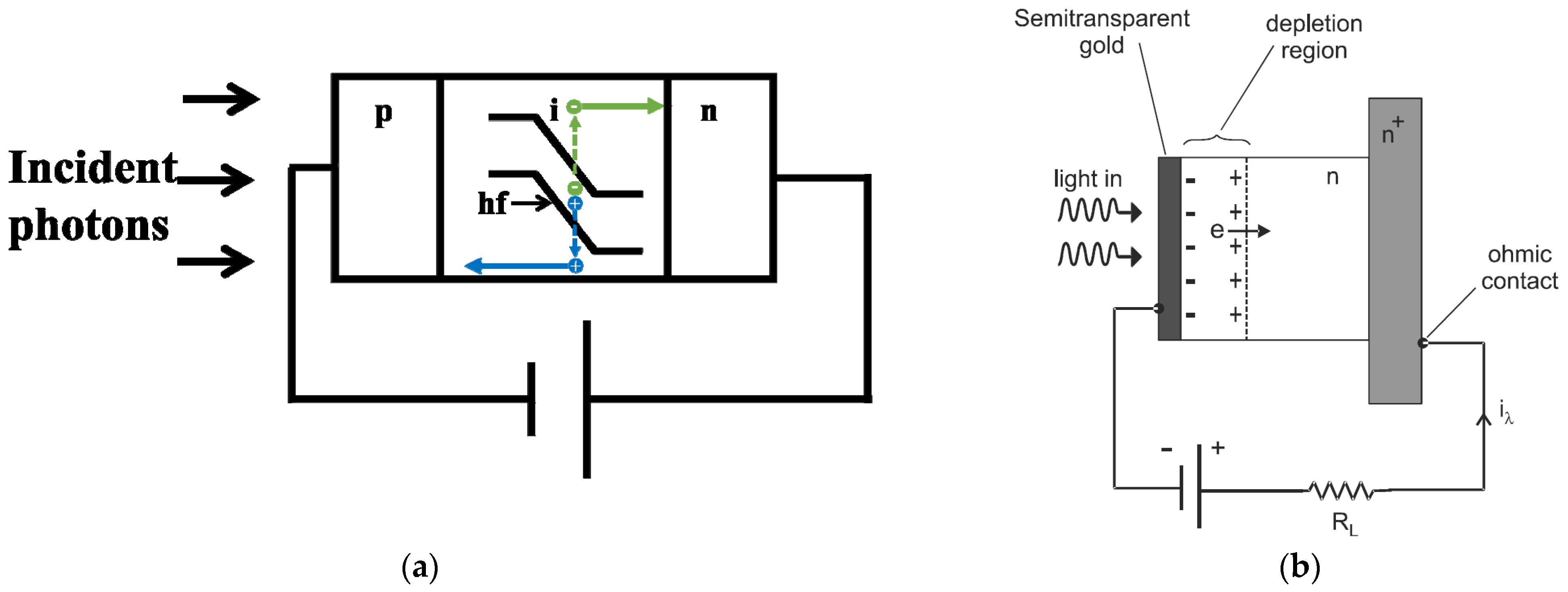
2.1. Photodetectors
2.2. Manipulation of Light by Optical Antennas
- (a)
- Near field scattering: in this scheme, optical antennas confine the incident light in the vicinity of the nanostructures, enhancing the light-matter interaction and promoting the transduction of photons into electric signals (Figure 2a). Mechanisms for near field scattering include surface plasmon resonance (SPR) and localized surface plasmon resonance (LSPR). SPRs arise from the coupling of electromagnetic fields to the oscillation of the electron plasma in metals, while LSPRs are non-propagating excitations of the conduction electrons in metallic nanostructures coupled to the electromagnetic fields [17].
- (b) Resonant detection: in this scheme, the incident light is coupled to the resonant modes in the nanostructured semiconductors and is absorbed efficiently due to the resonantly enhanced light-matter interaction (Figure 2b).
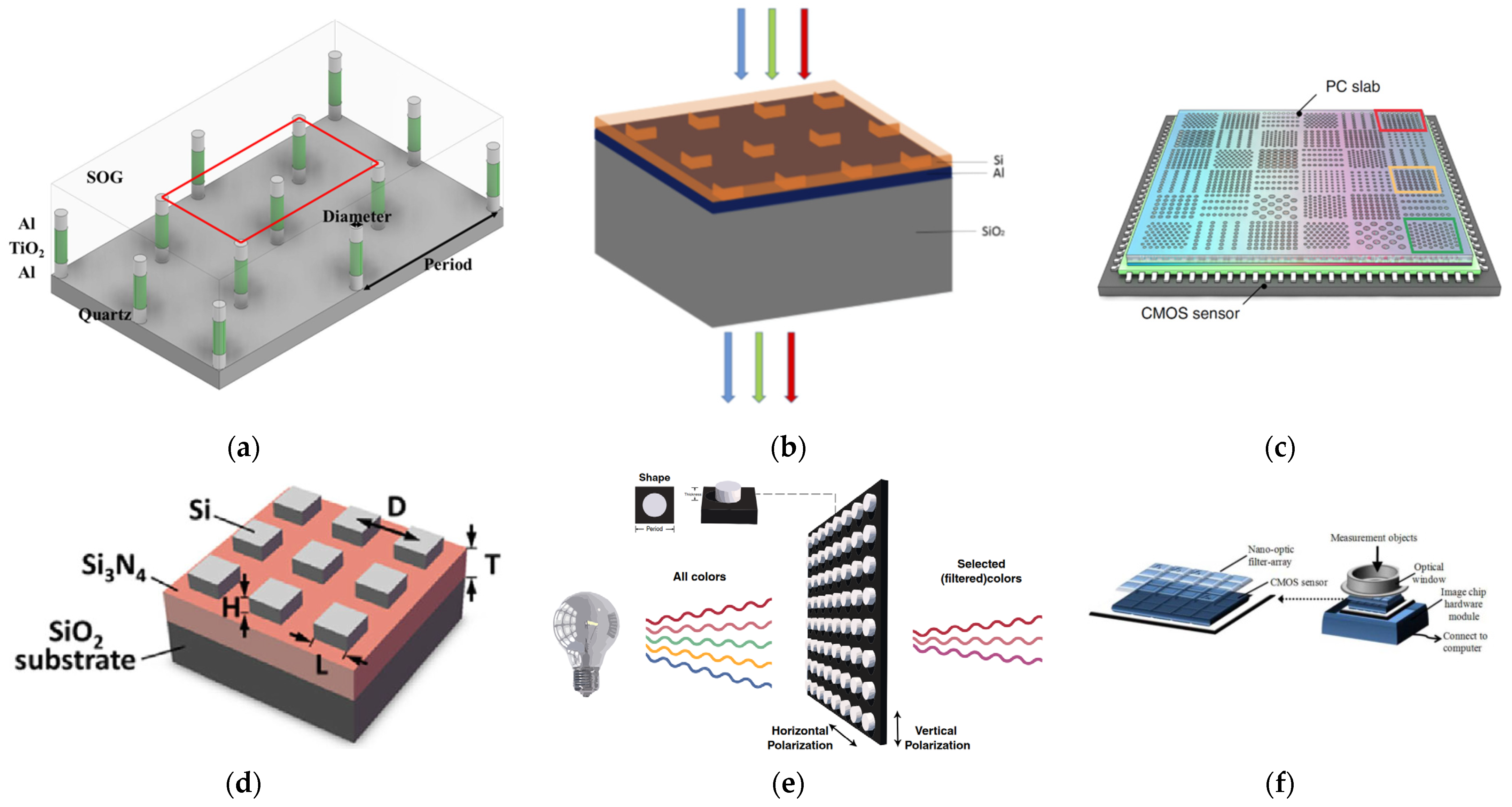
- (c) Far field scattering: in this scheme, the metasurfaces (arrays of optical antennas) collect and selectively scatter (or transmit) the incident light into far field, functioning as optical filters, polarizers, or other optical devices (Figure 2c).
3. Near-Field Scattering
3.1. SPRs Assisted QWIP
3.2. Plasmonic Nanoantenna Integrated Graphene Photodetector
3.3. LSPRs Assisted QWIP FPA
3.4. LSPRs Assisted HgTe Colloidal Quantum Dot Photodetector
3.5. Metamaterial Perfect Absorber (MPA) Schottky Photodetector
3.6. Plasmonic Antenna Integrated Stokes Polarimeter and Multi-Spectral Photodetector
4. Resonant Detection
4.1. Resonant Cavity-Enhanced Photodetector
4.2. Photon-Trapping Microstructures Assisted Photodetector
4.3. Nanowire Waveguide Photodetector
4.4. Anti-Hermitian Coupling Photodetector
5. Far-Field Scattering
5.1. Plasmonic Color Filter for Image Sensor
5.2. Coded Optical Filter for Hyperspectral Imaging
6. Discussion
Author Contributions
Funding
Conflicts of Interest
References
- Chee, K. Advances in Photodetectors—Research and Applications; IntechOpen: London, UK, 2019; ISBN 978-1-78985-622-4. [Google Scholar]
- Rogalski, A. Infrared and Terahertz Detectors, 3rd ed.; CRC Press: Boca Raton, FL, USA, 2018; ISBN 978-1-138-19800-5. [Google Scholar]
- Tan, X.; Zhang, H.; Li, J.; Wan, H.; Guo, Q.; Zhu, H.; Liu, H.; Yi, F. Non-Dispersive Infrared Multi-Gas Sensing via Nanoantenna Integrated Narrowband Detectors. Nat. Commun. 2020, 11, 5245. [Google Scholar] [CrossRef]
- Chen, H.-T.; Taylor, A.J.; Yu, N. A Review of Metasurfaces: Physics and Applications. Rep. Prog. Phys. 2016, 79, 076401. [Google Scholar] [CrossRef] [PubMed] [Green Version]
- Hsiao, H.-H.; Chu, C.H.; Tsai, D.P. Fundamentals and Applications of Metasurfaces. Small Methods 2017, 1, 1600064. [Google Scholar] [CrossRef] [Green Version]
- Capasso, F. The Future and Promise of Flat Optics: A Personal Perspective. Nanophotonics 2018, 7, 953–957. [Google Scholar] [CrossRef] [Green Version]
- Scheuer, J. Optical Metasurfaces Are Coming of Age: Short- and Long-Term Opportunities for Commercial Applications. ACS Photonics 2020, 7, 1323–1354. [Google Scholar] [CrossRef]
- Kamali, S.M.; Arbabi, E.; Arbabi, A.; Faraon, A. A Review of Dielectric Optical Metasurfaces for Wavefront Control. Nanophotonics 2018, 7, 1041–1068. [Google Scholar] [CrossRef]
- Li, J.; Bao, L.; Jiang, S.; Guo, Q.; Xu, D.; Xiong, B.; Zhang, G.; Yi, F. Inverse Design of Multifunctional Plasmonic Metamaterial Absorbers for Infrared Polarimetric Imaging. Opt. Express 2019, 27, 8375–8386. [Google Scholar] [CrossRef]
- Jiang, S.; Li, J.; Li, J.; Zhang, G.; Liu, H.; Yi, F. Genetic Optimization of Plasmonic Metamaterial Absorber towards Dual-Band Infrared Imaging Polarimetry. Opt. Express 2020, 28, 22617. [Google Scholar] [CrossRef] [PubMed]
- Quimby, R.S. Photonics and Lasers: An Introduction; John Wiley & Sons, Inc.: Hoboken, NJ, USA, 2006; ISBN 978-0-471-79159-1. [Google Scholar]
- Schneider, H.; Liu, H.C. Quantum Well Infrared Photodetectors: Physics and Applications; Springer Series in Optical Sciences; Springer: Berlin/Heidelberg, Germany, 2007; ISBN 978-3-540-36323-1. [Google Scholar]
- Xia, F.; Mueller, T.; Lin, Y.; Valdes-Garcia, A.; Avouris, P. Ultrafast Graphene Photodetector. Nat. Nanotechnol. 2009, 4, 839–843. [Google Scholar] [CrossRef] [Green Version]
- Stuart, H.R.; Hall, D.G. Absorption Enhancement in Silicon-on-insulator Waveguides Using Metal Island Films. Appl. Phys. Lett. 1996, 69, 2327–2329. [Google Scholar] [CrossRef]
- Codreanu, I.; Boreman, G.D. Infrared Microstrip Dipole Antennas—FDTD Predictions versus Experiment. Microw. Opt. Technol. Lett. 2001, 29, 381–383. [Google Scholar] [CrossRef]
- Bharadwaj, P.; Deutsch, B.; Novotny, L. Optical Antennas. Adv. Opt. Photonics 2009, 1, 438. [Google Scholar] [CrossRef] [Green Version]
- Maier, S.A. Plasmonics: Fundamentals and Applications; Springer: New York, NY, USA, 2007; ISBN 978-0-387-33150-8. [Google Scholar]
- Crozier, K.B.; Sundaramurthy, A.; Kino, G.S.; Quate, C.F. Optical Antennas: Resonators for Local Field Enhancement. J. Appl. Phys. 2003, 94, 4632–4642. [Google Scholar] [CrossRef]
- Tang, L.; Kocabas, S.E.; Latif, S.; Okyay, A.K.; Ly-Gagnon, D.-S.; Saraswat, K.C.; Miller, D.A.B. Nanometre-Scale Germanium Photodetector Enhanced by a near-Infrared Dipole Antenna. Nat. Photonics 2008, 2, 226–229. [Google Scholar] [CrossRef]
- Novotny, L.; van Hulst, N. Antennas for Light. Nat. Photonics 2011, 5, 83–90. [Google Scholar] [CrossRef]
- Cao, L.; Park, J.-S.; Fan, P.; Clemens, B.; Brongersma, M.L. Resonant Germanium Nanoantenna Photodetectors. Nano Lett. 2010, 10, 1229–1233. [Google Scholar] [CrossRef] [PubMed]
- Ebbesen, T.W.; Lezec, H.J.; Ghaemi, H.F.; Thio, T.; Wolff, P.A. Extraordinary Optical Transmission through Sub-Wavelength Hole Arrays. Nature 1998, 391, 667–669. [Google Scholar] [CrossRef]
- Burgos, S.P.; Yokogawa, S.; Atwater, H.A. Color Imaging via Nearest Neighbor Hole Coupling in Plasmonic Color Filters Integrated onto a Complementary Metal-Oxide Semiconductor Image Sensor. ACS Nano 2013, 7, 10038–10047. [Google Scholar] [CrossRef] [Green Version]
- Wu, W.; Bonakdar, A.; Mohseni, H. Plasmonic Enhanced Quantum Well Infrared Photodetector with High Detectivity. Appl. Phys. Lett. 2010, 96, 161107. [Google Scholar] [CrossRef] [Green Version]
- Yao, Y.; Shankar, R.; Rauter, P.; Song, Y.; Kong, J.; Loncar, M.; Capasso, F. High-Responsivity Mid-Infrared Graphene Detectors with Antenna-Enhanced Photocarrier Generation and Collection. Nano Lett. 2014, 14, 3749–3754. [Google Scholar] [CrossRef] [Green Version]
- Hutter, E.; Fendler, J.H. Exploitation of Localized Surface Plasmon Resonance. Adv. Mater. 2004, 16, 1685–1706. [Google Scholar] [CrossRef]
- Jing, Y.L.; Li, Z.F.; Li, Q.; Chen, X.S.; Chen, P.P.; Wang, H.; Li, M.Y.; Li, N.; Lu, W. Pixel-Level Plasmonic Microcavity Infrared Photodetector. Sci. Rep. 2016, 6, 25849. [Google Scholar] [CrossRef]
- Tang, X.; Ackerman, M.M.; Guyot-Sionnest, P. Thermal Imaging with Plasmon Resonance Enhanced HgTe Colloidal Quantum Dot Photovoltaic Devices. ACS Nano 2018, 12, 7362–7370. [Google Scholar] [CrossRef]
- Chang, C.-C.; Sharma, Y.D.; Kim, Y.-S.; Bur, J.A.; Shenoi, R.V.; Krishna, S.; Huang, D.; Lin, S.-Y. A Surface Plasmon Enhanced Infrared Photodetector Based on InAs Quantum Dots. Nano Lett. 2010, 10, 1704–1709. [Google Scholar] [CrossRef]
- Li, W.; Valentine, J. Metamaterial Perfect Absorber Based Hot Electron Photodetection. Nano Lett. 2014, 14, 3510–3514. [Google Scholar] [CrossRef] [PubMed]
- Zhou, Y.W.; Li, Z.F.; Zhou, J.; Li, N.; Zhou, X.H.; Chen, P.P.; Zheng, Y.L.; Chen, X.S.; Lu, W. High Extinction Ratio Super Pixel for Long Wavelength Infrared Polarization Imaging Detection Based on Plasmonic Microcavity Quantum Well Infrared Photodetectors. Sci. Rep. 2018, 8, 15070. [Google Scholar] [CrossRef] [PubMed] [Green Version]
- Li, W.; Coppens, Z.J.; Besteiro, L.V.; Wang, W.; Govorov, A.O.; Valentine, J. Circularly Polarized Light Detection with Hot Electrons in Chiral Plasmonic Metamaterials. Nat. Commun. 2015, 6, 8379. [Google Scholar] [CrossRef] [PubMed]
- Montoya, J.A.; Tian, Z.-B.; Krishna, S.; Padilla, W.J. Ultra-Thin Infrared Metamaterial Detector for Multicolor Imaging Applications. Opt. Express 2017, 25, 23343. [Google Scholar] [CrossRef] [PubMed]
- Yang, H.; Zheng, Y.; Li, N.; Wang, J.; Chen, P. Enhanced Terahertz Absorption of Quantum Wells Sandwiched between Heavily Doped Contacts Based on Micro-Cavity Resonance. J. Appl. Phys. 2020, 127, 053104. [Google Scholar] [CrossRef]
- Kishino, K.; Unlu, M.S.; Chyi, J.-I.; Reed, J.; Arsenault, L.; Morkoc, H. Resonant Cavity-Enhanced (RCE) Photodetectors. IEEE J. Quantum Electron. 1991, 27, 2025–2034. [Google Scholar] [CrossRef]
- Savich, G.R.; Wicks, G.W.; Jamison, K.; Fredin, L.; Golding, T.D.; Carmichael, M.; Reilly, J.; Craig, A.P.; Al-Saymari, F.; Marshall, A.R. Mid-Wavelength Infrared Resonant Cavity Enhanced Photodiodes for Infrared Spectroscopic Sensing of Chemicals and Other Narrow-Band Optical Signals. In Infrared Technology and Applications XLV, Proceedings of the SPIE Defense + Commercial Sensing, Baltimore, ML, USA, 14–18 April 2019; Fulop, G.F., Hanson, C.M., Andresen, B.F., Eds.; SPIE: Washington, DC, USA, 2019; p. 65. [Google Scholar]
- Park, G.C.; Taghizadeh, A.; Chung, I.-S. Hybrid Grating Reflectors: Origin of Ultrabroad Stopband. Appl. Phys. Lett. 2016, 108, 141108. [Google Scholar] [CrossRef] [Green Version]
- Craig, A.P.; Al-Saymari, F.; Jain, M.; Bainbridge, A.; Savich, G.R.; Golding, T.; Krier, A.; Wicks, G.W.; Marshall, A.R. Resonant Cavity Enhanced Photodiodes on GaSb for the Mid-Wave Infrared. Appl. Phys. Lett. 2019, 114, 151107. [Google Scholar] [CrossRef]
- Learkthanakhachon, S.; Taghizadeh, A.; Park, G.C.; Yvind, K.; Chung, I.-S. Hybrid III–V/SOI Resonant Cavity Enhanced Photodetector. Opt. Express 2016, 24, 16512–16519. [Google Scholar] [CrossRef] [Green Version]
- Lai, K.-W.; Lee, Y.-S.; Fu, Y.-J.; Lin, S.-D. Selecting Detection Wavelength of Resonant Cavity-Enhanced Photodetectors by Guided-Mode Resonance Reflectors. Opt. Express 2012, 20, 3572. [Google Scholar] [CrossRef] [Green Version]
- Gao, Y.; Cansizoglu, H.; Polat, K.G.; Ghandiparsi, S.; Kaya, A.; Mamtaz, H.H.; Mayet, A.S.; Wang, Y.; Zhang, X.; Yamada, T.; et al. Photon-Trapping Microstructures Enable High-Speed High-Efficiency Silicon Photodiodes. Nat. Photonics 2017, 11, 301–308. [Google Scholar] [CrossRef]
- Schmitt, S.W.; Sarau, G.; Christiansen, S. Observation of Strongly Enhanced Photoluminescence from Inverted Cone-Shaped Silicon Nanostructures. Sci. Rep. 2015, 5, 17089. [Google Scholar] [CrossRef] [PubMed] [Green Version]
- Vahala, K.J. Optical Microcavities. Nature 2003, 424, 839–846. [Google Scholar] [CrossRef]
- Kim, K.; Yoon, S.; Seo, M.; Lee, S.; Cho, H.; Meyyappan, M.; Baek, C.-K. Whispering Gallery Modes Enhance the Near-Infrared Photoresponse of Hourglass-Shaped Silicon Nanowire Photodiodes. Nat. Electron. 2019, 2, 572–579. [Google Scholar] [CrossRef]
- Pralle, M.U.; Vineis, C.; Palsule, C.; Jiang, J.; Carey, J.E. Ultra Low Light CMOS Image Sensors. In Infrared Technology and Applications XLVII, Proceedings of the SPIE Defense + Commercial Sensing, Online Only, FL, USA, 12–17 April 2021; Fulop, G.F., Kimata, M., Zheng, L., Andresen, B.F., Miller, J.L., Eds.; SPIE: Washington, DC, USA, 2021; p. 7. [Google Scholar]
- Huang, S.; Wu, Q.; Jia, Z.; Jin, X.; Fu, X.; Huang, H.; Zhang, X.; Yao, J.; Xu, J. Black Silicon Photodetector with Excellent Comprehensive Properties by Rapid Thermal Annealing and Hydrogenated Surface Passivation. Adv. Opt. Mater. 2020, 8, 1901808. [Google Scholar] [CrossRef]
- Wang, S.S.; Magnusson, R. Theory and Applications of Guided-Mode Resonance Filters. Appl. Opt. 1993, 32, 2606. [Google Scholar] [CrossRef]
- Verdun, M.; Portier, B.; Jaworowicz, K.; Jaeck, J.; Lelarge, F.; Guilet, S.; Dupuis, C.; Haïdar, R.; Pardo, F.; Pelouard, J.-L. Guided-Mode Resonator for Thin InGaAs P-i-N Short-Wave Infrared Photo-Diode. Appl. Phys. Lett. 2016, 108, 053501. [Google Scholar] [CrossRef]
- Gunapala, S.D.; Rafol, S.B.; Ting, D.Z.; Soibel, A.; Khoshakhlagh, A.; Keo, S.A.; Pepper, B.J.; Fisher, A.M.; Hill, C.J.; Choi, K.-K.; et al. T2SL Meta-Surfaced Digital Focal Plane Arrays for Earth Remote Sensing Applications. In Infrared Sensors, Devices, and Applications IX, Proceedings of the SPIE OPtical Engineering + Applications, San Diego, FL, USA, 11–15 August 2019; LeVan, P.D., Sood, A.K., Wijewarnasuriya, P., Eds.; SPIE: Washington, DC, USA, 2019; p. 9. [Google Scholar]
- Verdun, M.; Portier, B.; Jaworowicz, K.; Jaeck, J.; Dupuis, C.; Haidar, R.; Pardo, F.; Pelouard, J.-L. New Design of InGaAs Guided-Mode Resonance Photodiode for SWIR Low Dark Current Imaging. In Nanophotonics VI, Proceedings of the SPIE Photonics Europe, Brussels, Belgium, 3–7 April 2016; Andrews, D.L., Nunzi, J.-M., Ostendorf, A., Eds.; SPIE: Washington, DC, USA, 2016; Volume 9884, pp. 421–427. [Google Scholar]
- Fan, S.; Joannopoulos, J.D. Analysis of Guided Resonances in Photonic Crystal Slabs. Phys. Rev. B 2002, 65, 235112. [Google Scholar] [CrossRef] [Green Version]
- Kalchmair, S.; Gansch, R.; Ahn, S.I.; Andrews, A.M.; Detz, H.; Zederbauer, T.; Mujagić, E.; Reininger, P.; Lasser, G.; Schrenk, W.; et al. Detectivity Enhancement in Quantum Well Infrared Photodetectors Utilizing a Photonic Crystal Slab Resonator. Opt. Express OE 2012, 20, 5622–5628. [Google Scholar] [CrossRef] [PubMed]
- Sharma, G.; Bala, R. Digital Color Imaging Handbook; CRC Press: Boca Raton, FL, USA, 2017; ISBN 978-1-351-83597-8. [Google Scholar]
- Bayer, B.E. Color Imaging Array. U.S. Patent US3971065A, 20 July 1976. [Google Scholar]
- Wang, B.; Leu, P.W. Tunable and Selective Resonant Absorption in Vertical Nanowires. Opt. Lett. 2012, 37, 3756. [Google Scholar] [CrossRef] [PubMed]
- Park, H.; Dan, Y.; Seo, K.; Yu, Y.J.; Duane, P.K.; Wober, M.; Crozier, K.B. Filter-Free Image Sensor Pixels Comprising Silicon Nanowires with Selective Color Absorption. Nano Lett. 2014, 14, 1804–1809. [Google Scholar] [CrossRef]
- Meng, J.; Cadusch, J.J.; Crozier, K.B. Detector-Only Spectrometer Based on Structurally Colored Silicon Nanowires and a Reconstruction Algorithm. Nano Lett. 2019, 20, 320–328. [Google Scholar] [CrossRef] [PubMed]
- Zhang, S.; Ye, Z.; Wang, Y.; Park, Y.; Bartal, G.; Mrejen, M.; Yin, X.; Zhang, X. Anti-Hermitian Plasmon Coupling of an Array of Gold Thin-Film Antennas for Controlling Light at the Nanoscale. Phys. Rev. Lett. 2012, 109, 193902. [Google Scholar] [CrossRef] [Green Version]
- Kim, S.J.; Kang, J.-H.; Mutlu, M.; Park, J.; Park, W.; Goodson, K.E.; Sinclair, R.; Fan, S.; Kik, P.G.; Brongersma, M.L. Anti-Hermitian Photodetector Facilitating Efficient Subwavelength Photon Sorting. Nat. Commun. 2018, 9, 316. [Google Scholar] [CrossRef] [PubMed] [Green Version]
- Smalley, J.S.T.; Ren, X.; Lee, J.Y.; Ko, W.; Joo, W.-J.; Park, H.; Yang, S.; Wang, Y.; Lee, C.S.; Choo, H.; et al. Subwavelength Pixelated CMOS Color Sensors Based on Anti-Hermitian Metasurface. Nat. Commun. 2020, 11, 3916. [Google Scholar] [CrossRef]
- Brewer, T.L.; Hawley, D.W.; Lamb, J.E.; Latham, W.J.; Stichnote, L.K. Light Filters for Microelectronics. European Patent EP0298116B1, 27 August 1997. [Google Scholar]
- Yokogawa, S.; Burgos, S.P.; Atwater, H.A. Plasmonic Color Filters for CMOS Image Sensor Applications. Nano Lett. 2012, 12, 4349–4354. [Google Scholar] [CrossRef]
- Yu, Y.; Chen, Q.; Wen, L.; Hu, X.; Zhang, H.-F. Spatial Optical Crosstalk in CMOS Image Sensors Integrated with Plasmonic Color Filters. Opt. Express 2015, 23, 21994. [Google Scholar] [CrossRef]
- He, X.; Liu, Y.; Uddin, H.; Nirmalathas, A.; Unnithan, R.R. Integration of Angle Independent CMY Nanorod Colour Filter Mosaic on CMOS Image Sensor. In Proceedings of the Conference on Lasers and Electro-Optics, Washington, DC, USA, 10–15 May 2020; OSA: Washington, DC, USA, 2020; p. JTu2D.22. [Google Scholar]
- He, X.; Liu, Y.; Beckett, P.; Uddin, H.; Nirmalathas, A.; Unnithan, R.R. CMY Camera Using a Nanorod Filter Mosaic Integrated on a CMOS Image Sensor. OSA Contin. OSAC 2021, 4, 229–238. [Google Scholar] [CrossRef]
- West, M.; Grossmann, J.; Galvan, C. Commercial Snapshot Spectral Imaging: The Art of the Possible; MITRE: McLean, VA, USA, 2018; 42p. [Google Scholar]
- Bao, J.; Bawendi, M.G. A Colloidal Quantum Dot Spectrometer. Nature 2015, 523, 67–70. [Google Scholar] [CrossRef]
- Wang, X.; Thomas, J.-B.; Hardeberg, J.Y.; Gouton, P. Multispectral Imaging: Narrow or Wide Band Filters? J. Int. Colour Assoc. 2014, 12, 44–51. [Google Scholar]
- Li, S. Superiority of Optimal Broadband Filter Sets under Lower Noise Levels in Multispectral Color Imaging. Color Res. Appl. 2021, 46, 783–790. [Google Scholar] [CrossRef]
- Oliver, J.; Lee, W.; Park, S.; Lee, H.-N. Improving Resolution of Miniature Spectrometers by Exploiting Sparse Nature of Signals. Opt. Express 2012, 20, 2613. [Google Scholar] [CrossRef] [PubMed]
- Oliver, J.; Lee, W.-B.; Lee, H.-N. Filters with Random Transmittance for Improving Resolution in Filter-Array-Based Spectrometers. Opt. Express 2013, 21, 3969. [Google Scholar] [CrossRef]
- Wu, X.; Gao, D.; Chen, Q.; Chen, J. Multispectral Imaging via Nanostructured Random Broadband Filtering. Opt. Express 2020, 28, 4859. [Google Scholar] [CrossRef] [PubMed]
- Wang, Z.; Yi, S.; Chen, A.; Zhou, M.; Luk, T.S.; James, A.; Nogan, J.; Ross, W.; Joe, G.; Shahsafi, A.; et al. Single-Shot on-Chip Spectral Sensors Based on Photonic Crystal Slabs. Nat. Commun. 2019, 10, 1020. [Google Scholar] [CrossRef] [PubMed]
- Song, H.; Ma, Y.; Han, Y.; Shen, W.; Zhang, W.; Li, Y.; Liu, X.; Peng, Y.; Hao, X. Deep-Learned Broadband Encoding Stochastic Filters for Computational Spectroscopic Instruments. Adv. Theory Simul. 2021, 4, 2000299. [Google Scholar] [CrossRef]
- Han, X.; Fan, Z.; Liu, Z.; Li, C.; Guo, L.J. Inverse Design of Metasurface Optical Filters Using Deep Neural Network with High Degrees of Freedom. InfoMat 2021, 3, 432–442. [Google Scholar] [CrossRef]
- Kurokawa, U.; Choi, B.I.; Chang, C.-C. Filter-Based Miniature Spectrometers: Spectrum Reconstruction Using Adaptive Regularization. IEEE Sens. J. 2011, 11, 1556–1563. [Google Scholar] [CrossRef]


Publisher’s Note: MDPI stays neutral with regard to jurisdictional claims in published maps and institutional affiliations. |
© 2021 by the authors. Licensee MDPI, Basel, Switzerland. This article is an open access article distributed under the terms and conditions of the Creative Commons Attribution (CC BY) license (https://creativecommons.org/licenses/by/4.0/).
Share and Cite
Li, J.; Li, J.; Zhou, S.; Yi, F. Metasurface Photodetectors. Micromachines 2021, 12, 1584. https://doi.org/10.3390/mi12121584
Li J, Li J, Zhou S, Yi F. Metasurface Photodetectors. Micromachines. 2021; 12(12):1584. https://doi.org/10.3390/mi12121584
Chicago/Turabian StyleLi, Jinzhao, Junyu Li, Shudao Zhou, and Fei Yi. 2021. "Metasurface Photodetectors" Micromachines 12, no. 12: 1584. https://doi.org/10.3390/mi12121584