1. Introduction
The modular multilevel converter (MMC) is considered to be the most promising multilevel power converter in medium and high voltage applications. It has the advantages of modularity, low switching frequency, low harmonic distortion and expandability [
1,
2]. These excellent characteristics enable the MMC to be applied to high-voltage DC (HVDC) transmission, the static synchronous compensator (STATCOM), high-power motor drive and the unified power flow controller (UPFC) [
3,
4,
5,
6]. The research on the MMC mainly focus on the capacitor voltage balance strategy of submodules, the circulating current control algorithm and the modulation method [
1].
The output waveform quality and the switching loss are directly affected by the modulation method. Thus, various modulation methods have been proposed for MMC, such as carrier-based pulse width modulation, space vector pulse width modulation (SVPWM), nearest level modulation (NLM) and selective harmonic elimination (SHE) [
7,
8,
9,
10,
11]. More submodules need to be connected in series if the MMC is adapted to high voltage application. Thus, the switching loss needs to be considered a key issue.
Discontinuous pulse width modulation (DPWM) can clamp the output voltage of a certain phase to the DC bus in each fundamental period to reduce the switching loss. In [
12], an improved DPWM method is proposed to modify the reference voltage of each submodule by splitting and rotating discontinuous modulated waves, which solves the problem of unbalanced power distribution among submodules. However, the output waveform quality is poor and the capacitor voltage ripple of submodules is large. Moreover, the control complexity increases with the increase in the number of submodules. In [
13], a DPWM method with zero-sequence voltage injection is proposed, which reduced the capacitor voltage ripple and switching loss of the submodule. However, this scheme requires redundant submodules to prevent overmodulation. In [
14], a DPWM method based on the space vector concept is proposed. The zero-sequence voltage can be determined based on the position of the two-level space vector. This method only uses the two-level space vector and the clamping interval width cannot be changed. In [
15], a model predictive control technology based on the DPWM scheme is proposed to reduce the switching loss of the submodules, but the algorithm is complex.
In this paper, a discontinuous modulation method with variable clamping interval width is proposed. The influence of power factor on output current phase is considered, and different clamping interval positions can be determined by the selection of different zero-sequence components. The width of the clamping interval can also be changed according to the requirement of the switching loss and the output waveform quality.
2. Principle of Modular Multilevel Converter
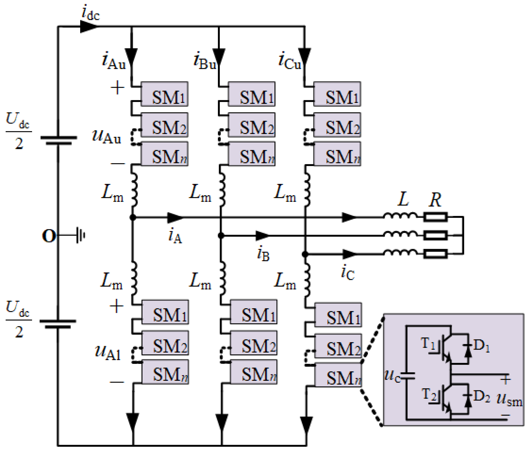
The topology of the three-phase MMC is shown in
Figure 1. The upper and lower arms of each phase are composed of several half-bridge submodules and arm inductors in series. The switching state of power devices of each submodule and the corresponding output voltage of the submodule are shown in
Table 1. If T
1 is ON and T
2 is OFF, the state of the submodule is defined as ON, and the output voltage of the submodule is
uc; on the contrary, if T
1 is OFF and T
2 is ON, the state of the submodule is defined as OFF, and the output voltage of the submodule is 0.
The total output voltage of the submodules of the upper and lower arms of any phase in the MMC can be expressed as:
where
x∈{A, B, C}, u and l represent upper and lower arms, respectively,
h represents the
h-th submodule and
h∈{1, 2,...,
n}.
Taking Phase A as an example, ignoring the voltage drop of arm inductance, the following expression can be obtained from Kirchhoff’s voltage law:
The output voltage of Phase A can be expressed as:
Similarly, the arm current can be expressed as:
where
ix and
ixz are the phase current and differential current flowing through the arm, which can be expressed as:
3. Conventional Discontinuous Modulation Method
Each phase of the MMC can be clamped to the DC bus by injecting discontinuous zero-sequence voltage into the three-phase reference voltage. If any phase is clamped to the DC bus, the switching state of the corresponding power device will remain unchanged, and the switching loss will be significantly reduced. For the MMC, when the upper and lower arm of any arbitrary phase are in the clamping state, the submodule of the arm is bypassed and the submodule has no switching action, which significantly reduces the switching loss. Due to the specific topology of the MMC, no current flows through the capacitors in the bypassed submodules. As a result, the voltage fluctuation of capacitors is reduced.
The three-phase reference voltage of the MMC can be expressed as:
where
ω is the frequency of the reference voltage and
m is the modulation index, which is defined as:
where
Um is the amplitude of the reference voltage.
The reference voltage after zero-sequence component injection can be expressed as:
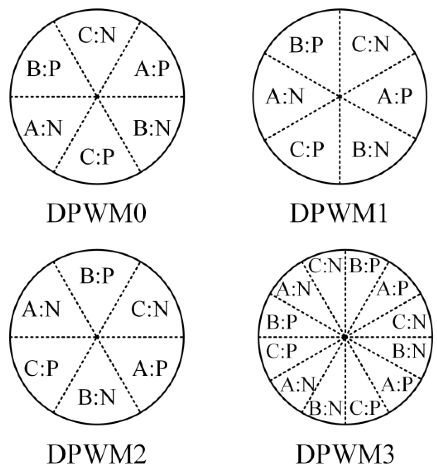
Conventional discontinuous modulation methods can be classified into four types: DPWM0~DPWM3 (as shown in
Figure 2). A, B and C represent the clamping phase, P represents the phase is clamped to the positive DC bus and N indicates that the phase is clamped to the negative DC bus.
According to the division of clamping interval in
Figure 2, let us take Phase A as an example.
λ is defined as the clamping factor.
λ is equal to 1 when Phase A is in the clamping interval. While
λ is equal to 0 when Phase A is in the non-clamping interval. The value of
λ in each sector for DPWM0~DPWM3 is shown in
Figure 3. Then the expression of zero-sequence voltage can be expressed as:
where
umax = max{
uA,
uB,
uC} and
umin = min{
uA,
uB,
uC}. Thus, the expression of zero-sequence voltage can be further expressed as:
4. Discontinuous Modulation Method with Variable Clamping Interval
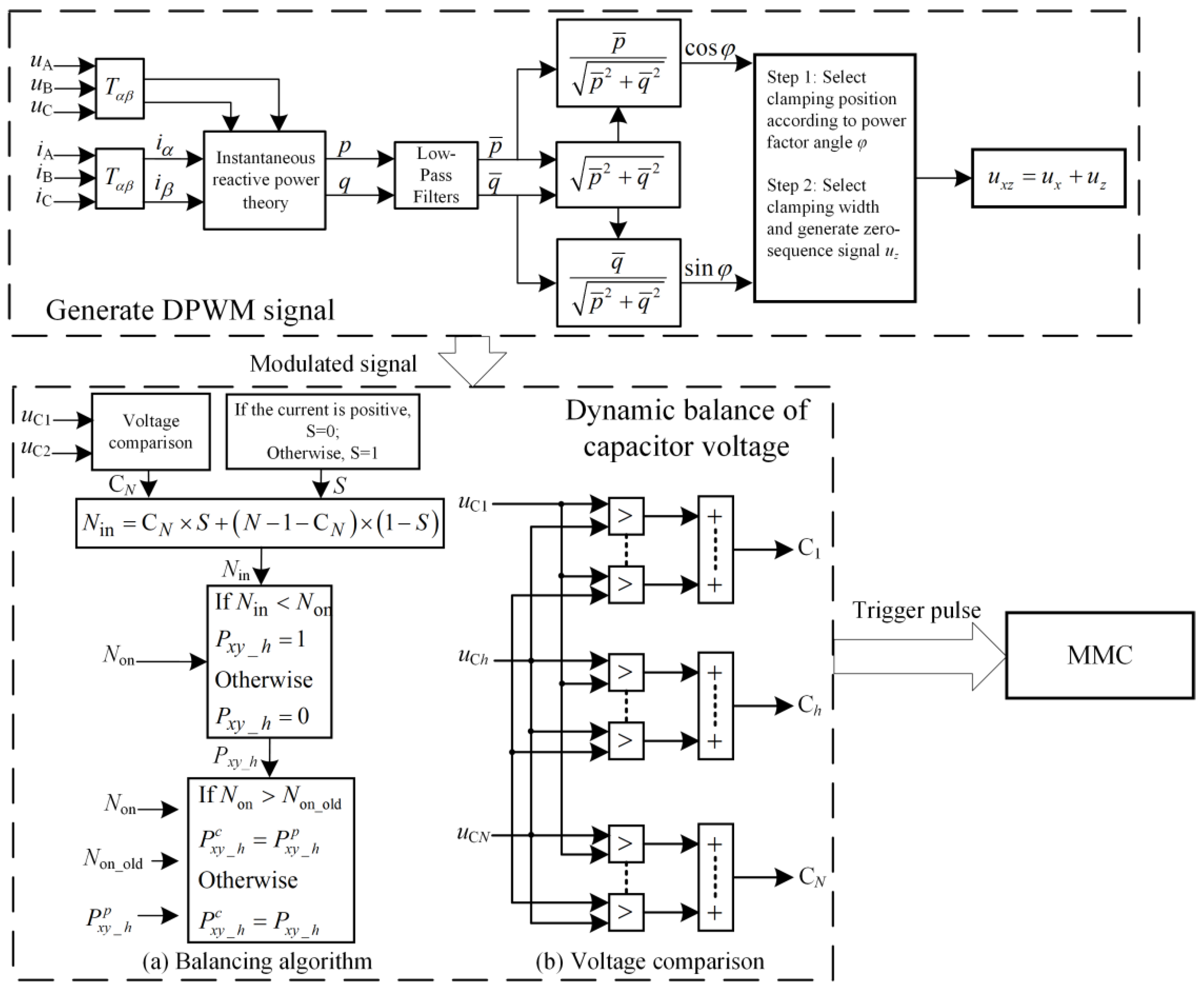
Conventional discontinuous modulation methods clamp the switching state in a fixed interval in each fundamental cycle. If the power factor changes, the switching loss will be increased. In this paper, an improved discontinuous modulation strategy is proposed. Each phase can be clamped to the DC bus at the maximum value of load current by adjusting the clamping interval online. Thus, the switching loss and the voltage fluctuation of the submodule can be reduced. The overall control flow diagram of the system is shown in
Figure 4.
4.1. Calculation of Power Factor
The power factor can be calculated by the instantaneous reactive power theory [
16]. The DC components of reactive power and active power can be separated and then the power factor can be calculated.
The phase of the original reference voltage signal can be shifted according to the calculated power factor angle
φ. Thus:
The maximum and minimum value of the reference voltage signal after phase shifting can be defined as:
4.2. Discontinuous Modulation Method with Variable Clamping Interval
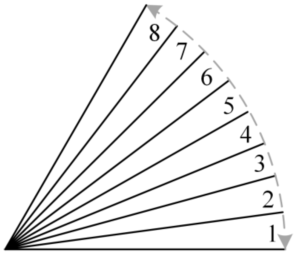
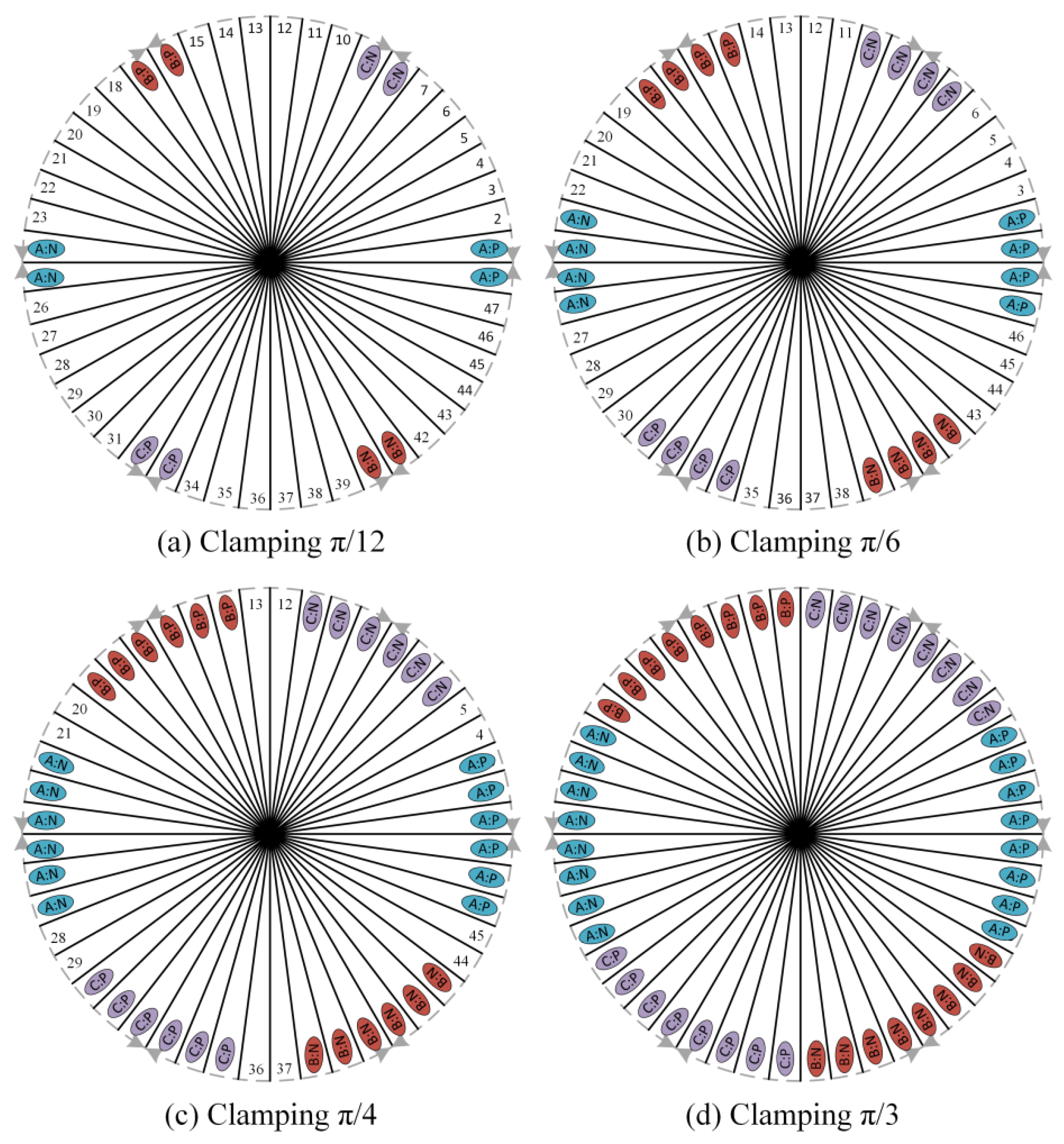
The change of clamping interval will lead to the change of switching loss and output waveform quality. In industrial applications, different widths of the clamping interval need to be selected according to the requirements of the system. To achieve variable width of the clamping interval, each sector is further divided into eight subregions with an interval of π/24, as shown in
Figure 5. Each subregion can be independently set as a clamping interval or an unclamping interval.
In the unclamp interval, the zero-sequence component
uz = 0, while in the clamping interval:
The clamping interval and the unclamping interval can be flexibly selected. It does not require complex coordinate transformation, trigonometric function calculation, vector selection and duty cycle calculation.
Figure 6 shows the discontinuous modulation methods with four clamping interval widths: π/12, π/6, π/4 and π/3.
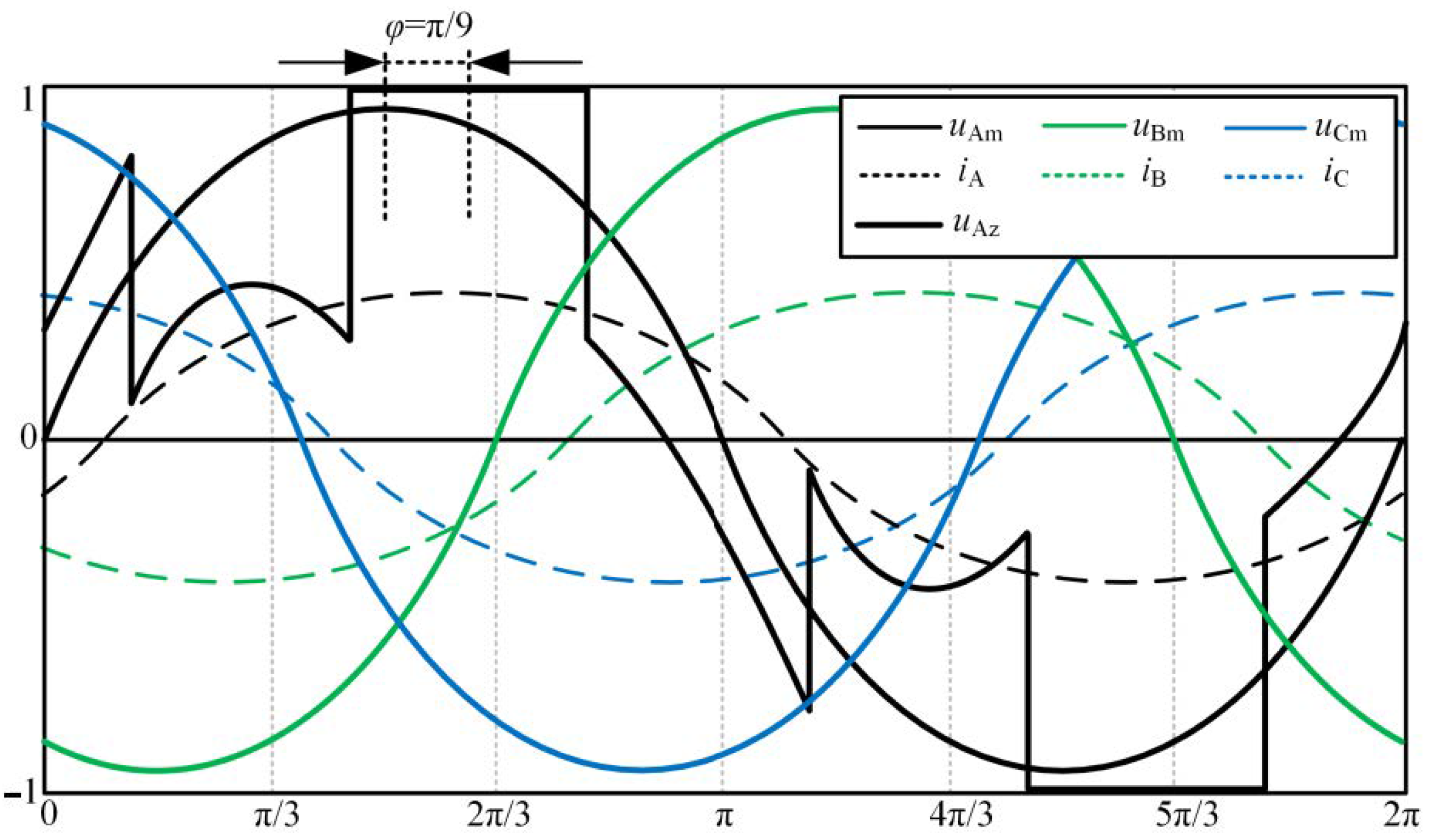
Taking power factor angle
φ = π/9 as an example, the variable load power factor discontinuous modulation voltage is shown in
Figure 7. When the amplitude of the load current is close to its peak value, the corresponding phase is clamped to the DC bus. The switching loss can effectively be reduced.
4.3. Capacitor Voltage Dynamic Balance Algorithm
In order to solve the power imbalance problem of submodule, the capacitor voltage dynamic balance algorithm needs to be adopted. The ON and OFF of submodules are determined by the direction of the arm current and the capacitor voltage of submodules. The algorithm can be divided into the following steps (as shown in
Figure 4):
- (1)
Determining the total number of submodules which need to be put in, then subsequently sorting the submodules into numerical order according to the amplitude of the capacitor voltage;
- (2)
Judging the direction of the current ixy. When the direction of ixy is positive, set S = 0, otherwise, set S = 1;
- (3)
Determining the index number of submodules according to the direction of
ixy. The expression of the index number is as follows:
- (4)
The ON and OFF of each submodule is determined by the calculation result of step (3);
- (5)
Judging the change of the number of submodules in the ON state. If the number of submodules in the ON state is not changed, there will be no switching behavior, and the switching loss will be reduced.
In the clamping interval, the number of submodules in the ON state is constant, and the dynamic balance algorithm of the capacitor voltage is not applied.
5. Experimental Verification
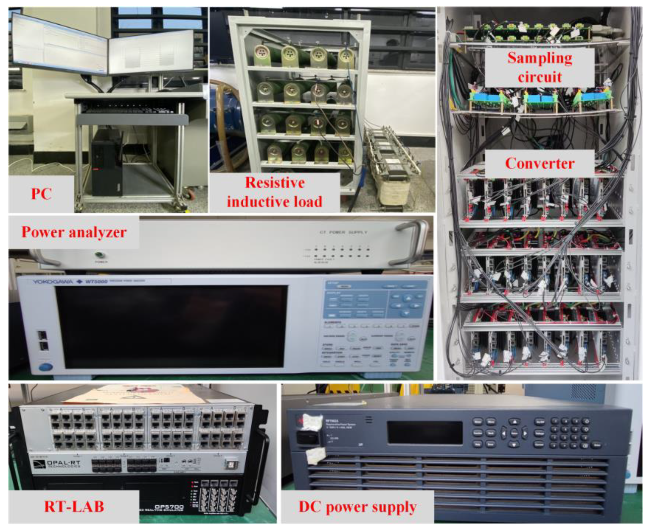
In order to verify the feasibility and effectiveness of the proposed modulation method, the rapid control prototype OP5700 (OPAL-RT Co. Ltd. Montreal, Quebec, Canada) and the H-bridge power model PEH2015 (Imperix Co. Ltd., Sion, Switzerland) are adopted to establish the experimental setup, as shown in
Figure 8.
The proposed modulation strategy is tested under eight different clamping interval conditions (π/24, π/12, π/8, π/6, 5π/24, π/4, 7π/24 and π/3). The parameters of the experimental setup are listed in
Table 2.
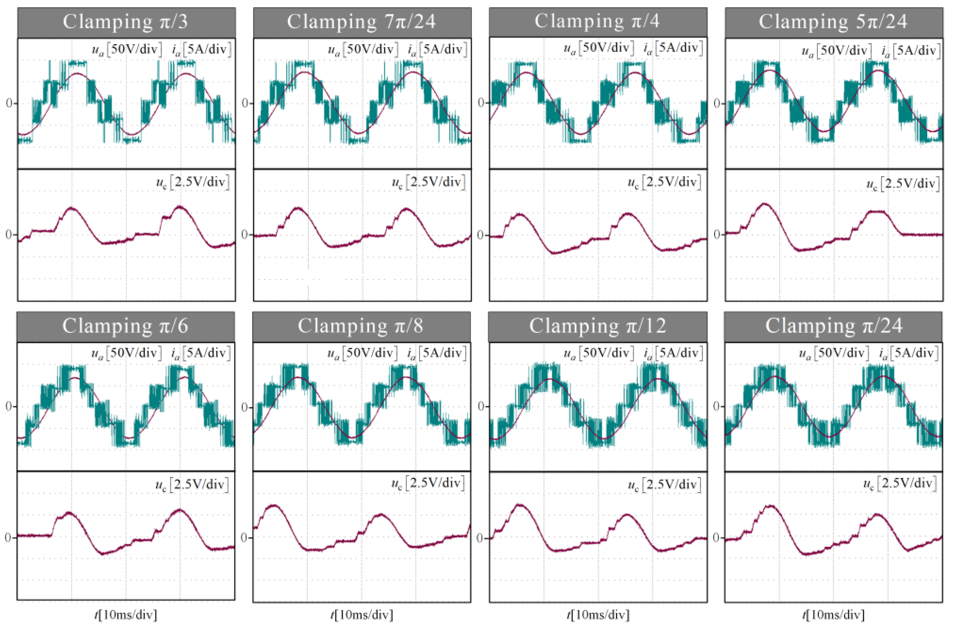
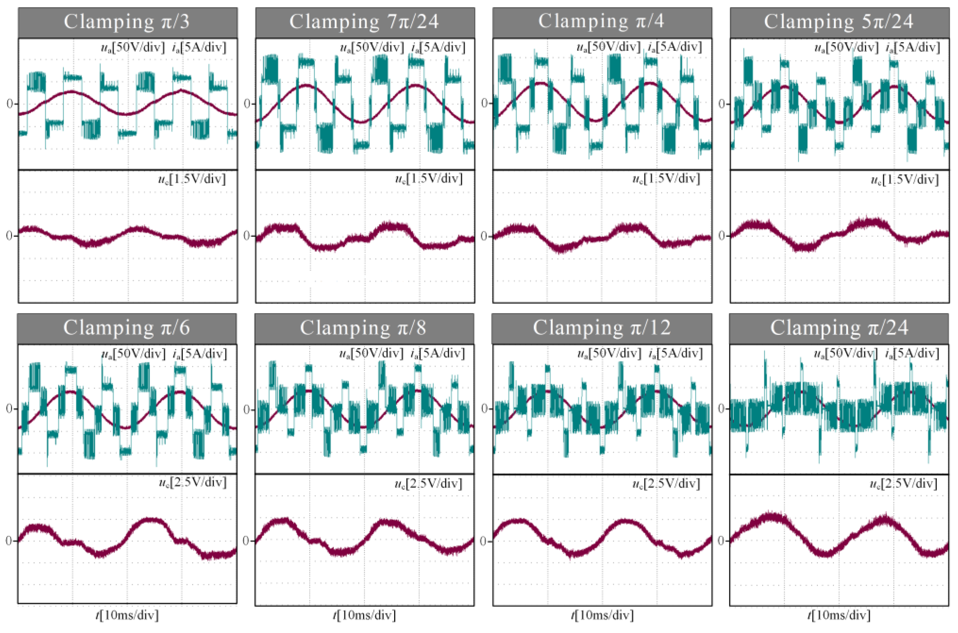
Figure 9 and
Figure 10 shows the output current, phase voltage and capacitor voltage ripple of eight different clamping intervals (π/24 to π/3) under the condition of
m = 0.9 and
m = 0.3. As can be seen, no matter how the width of the clamping interval changes, the output current remains sinusoidal. With the decrease in the width of the clamping interval, the capacitor voltage ripple of the submodule increases.
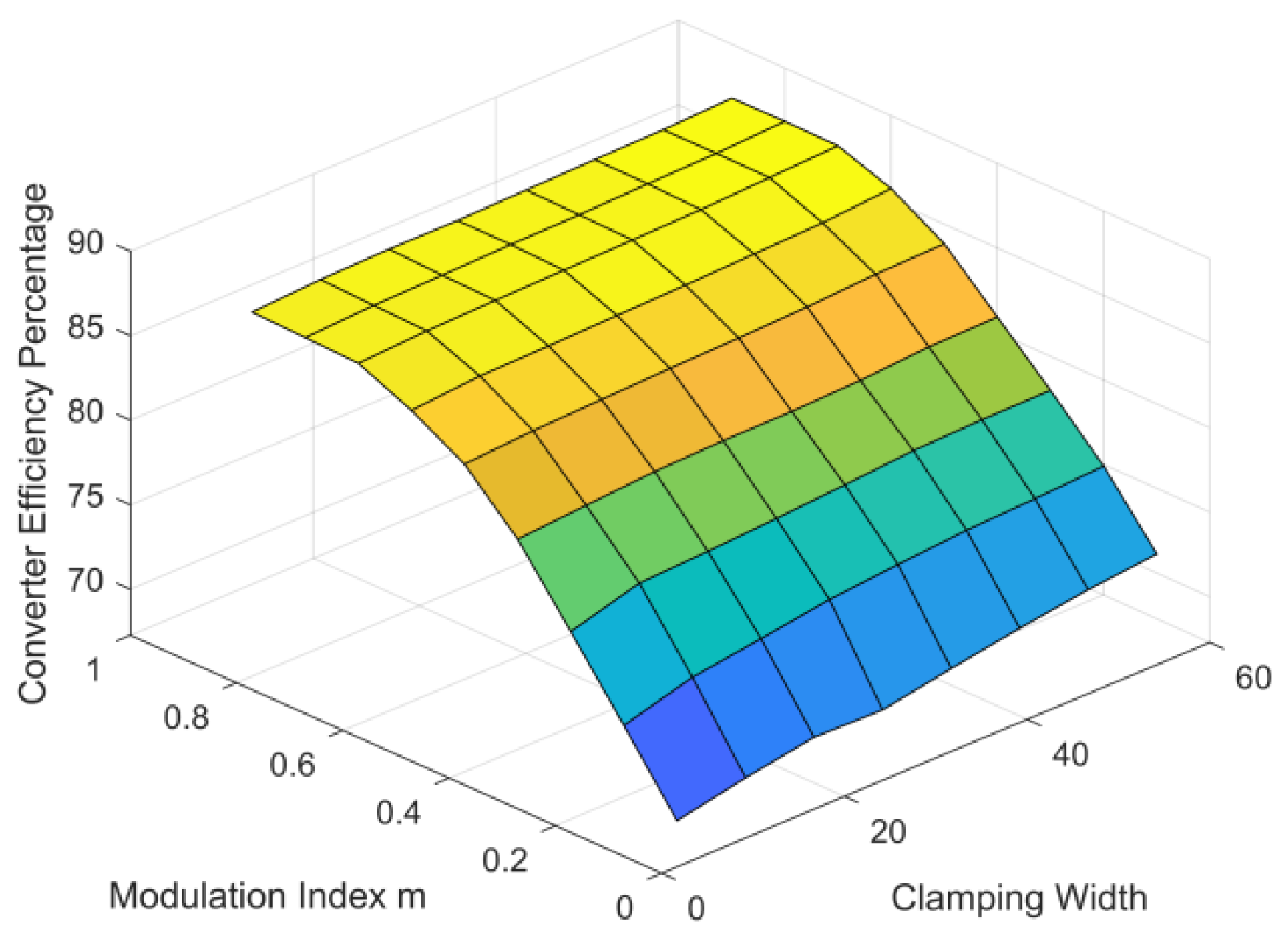
5.1. Switching Loss
The efficiency of the proposed modulation strategy under different modulation indices and clamping interval width conditions is recorded by a Yokogawa WT5000 power analyzer. The variation of efficiency with the change of the modulation index and the width of the clamping interval is shown in
Figure 11.
Under lower modulation index conditions, the efficiency is gradually improved with the increase in clamping width. While under higher modulation index conditions, the change of the efficiency is unobvious.
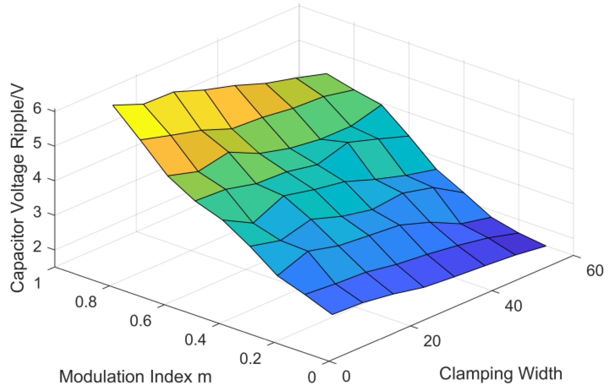
5.2. Capacitor Voltage Ripple of Submodule
The variation of the capacitor voltage ripple with the change of the modulation index and the width of the clamping interval is shown in
Figure 12.
As shown in
Figure 12, under the same modulation index, the capacitance voltage ripple decreases continuously with the increase in the width of the clamping interval from π/24 to π/3. This is because there is no current flowing through the capacitor of the submodule during the clamping interval.
5.3. Total Harmonic Distortion
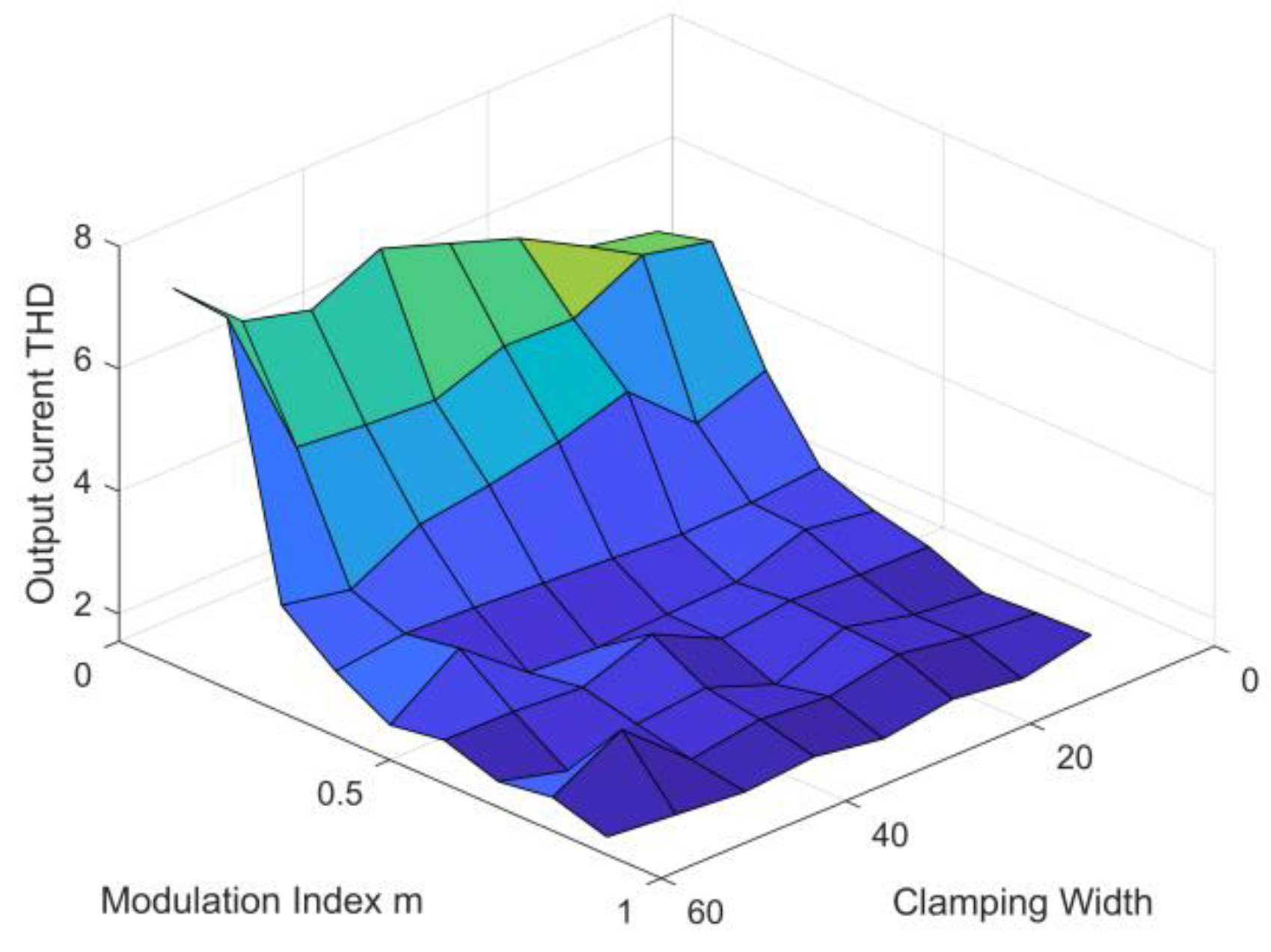
The variation of total harmonic distortion (THD) of the output current with the change of the modulation index and the width of the clamping interval is shown in
Figure 13.
Under lower modulation index conditions, the THD of the output current raises with the increase in clamping width. While under higher modulation index conditions, the change of the THD of the output current is unobvious.
In conclusion, under higher modulation index conditions, the change of the width of the clamping interval will not lead to a rapid variation of the THD of the output current and the switching loss. Under lower modulation index conditions, the switching loss can be effectively reduced by broadening the clamping interval. In addition, the variation of the THD of the output current is simultaneously unobvious.
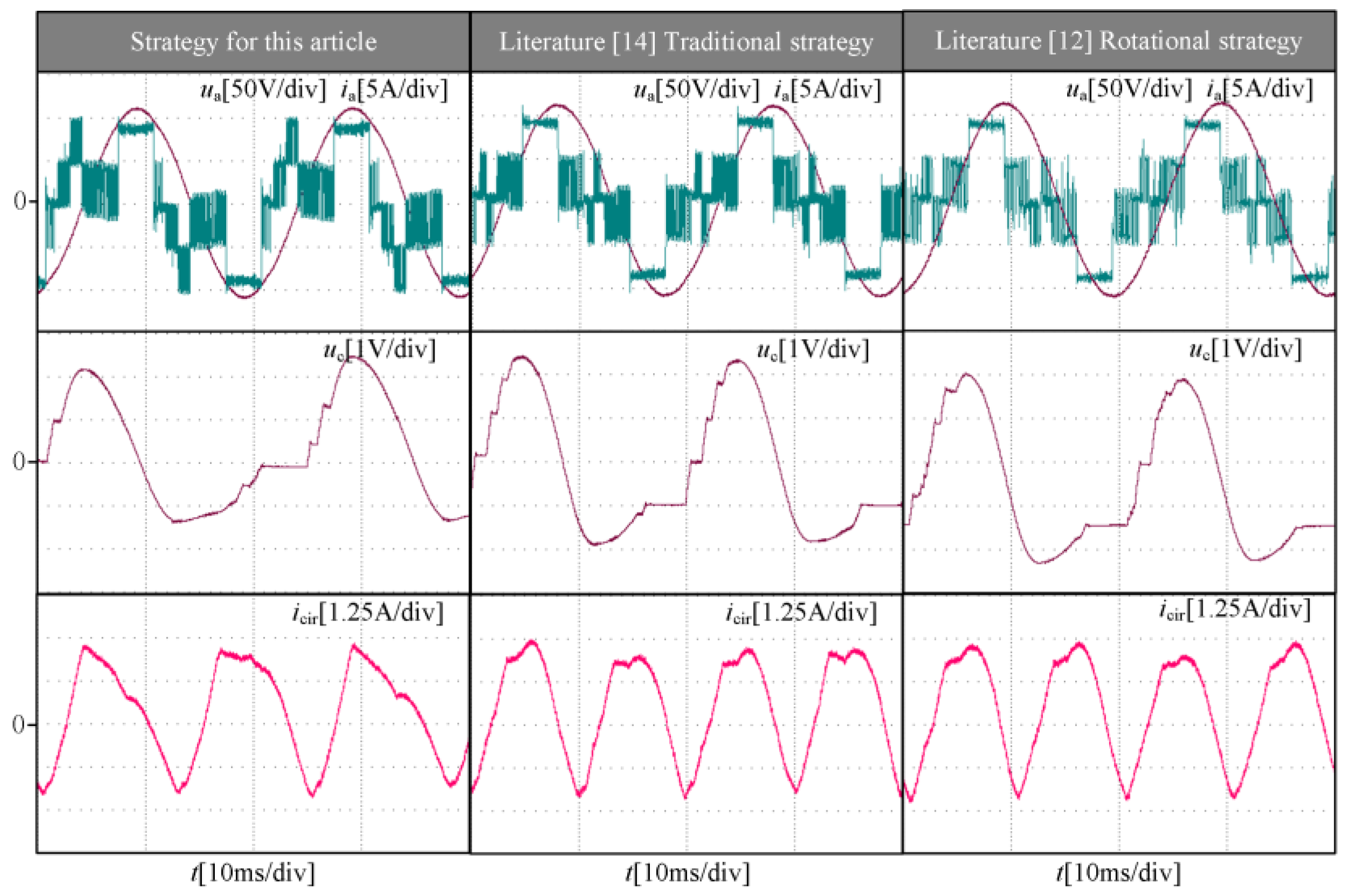
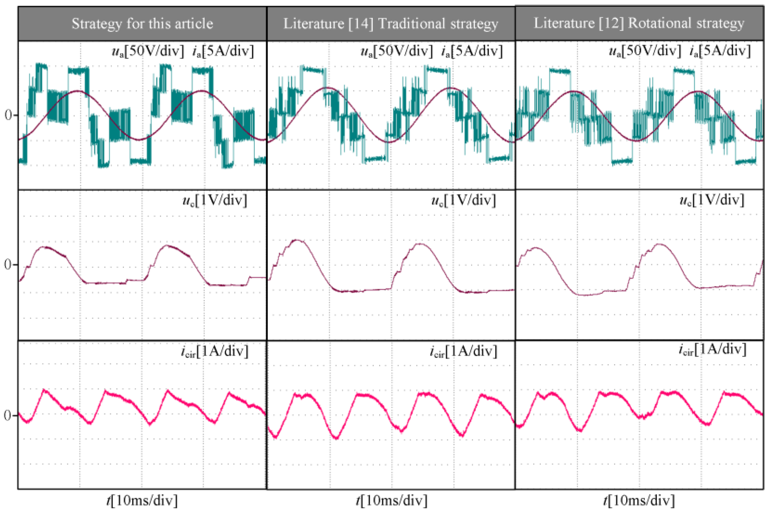
5.4. Strategy Comparison
To verify the effectiveness of the algorithm in this paper, the proposed strategy is compared with the conventional strategy and the rotation strategy. Comparison experiments were performed at a clamping width of π/3 and
m = 0.8.
Figure 14 shows the output current, phase voltage, capacitor voltage ripple and circulating current under the condition of 5 Ω and 10 mH. The proposed strategy reduces capacitor voltage fluctuations and circulating current.
As shown in
Figure 15, under the condition of 10 Ω and 30 mH, the effect of the proposed strategy is the same.
6. Conclusions
In this paper, a discontinuous modulation method with variable clamping interval width of the MMC for different load power factor conditions is proposed. The position of the clamping interval can be adjusted according to the power factor. In addition, the width of the clamping interval can also be adjusted according to the requirements of switching loss and the output waveform quality. The proposed method is tested and verified by a RT-LAB based rapid prototype development experimental system. The results show that the switching loss can be significantly reduced without reducing the output waveform quality under lower modulation conditions.
Author Contributions
Conceptualization, G.Z. and X.G.; methodology, L.M. and X.G.; software, L.M.; validation, L.M. and X.J.; formal analysis, L.M. and X.G.; writing—original draft preparation, L.M.; writing—review and editing, X.G., and G.Z.; funding acquisition, X.G. and G.Z. All authors have read and agreed to the published version of the manuscript.
Funding
This research was funded by “The National Natural Science Foundation of China, grant number 52177055”, “The Zhejiang Provincial Basic Public Welfare Research Projects, grant number LGG22E070011”.
Institutional Review Board Statement
Not applicable.
Informed Consent Statement
Not applicable.
Data Availability Statement
Not applicable.
Conflicts of Interest
The authors declare no conflict of interest.
References
- Lv, G.T.; Lei, W.J.; Wang, M. Reliability Analysis and Design of MMC Based on Mission Profile for the Components Degradation. IEEE Access 2020, 8, 149940–149951. [Google Scholar] [CrossRef]
- Tian, Y.M.; Wickramasinghe, H.-R.; Li, Z.X. Review, Classification and Loss Comparison of Modular Multilevel Converter Submodules for HVDC Applications. Energies 2022, 15, 1985. [Google Scholar] [CrossRef]
- Guo, J.; Jiang, D.Z.; Zhou, Y.B. Energy storable VSC-HVDC system based on modular multilevel converter. Int. J. Elec. Power 2016, 78, 269–276. [Google Scholar] [CrossRef]
- Franquelo, L.-G.; Rodriguez, J.; Leon, J.-I. The Age of Multilevel Converters Arrives. IEEE Ind. Electron. Mag. 2008, 2, 28–39. [Google Scholar] [CrossRef] [Green Version]
- Xu, Q.M.; Ma, F.J.; He, Z.X. Double Star Multilevel Railway Power Regulator and Its Control Method. Proc. CSEE 2016, 36, 3609–3618. [Google Scholar]
- Tang, G.F.; Luo, X.; Wei, X.G. Multi-terminal DC transmission and DC network technology. Proc. CSEE 2013, 33, 8–17. [Google Scholar]
- Moranchel, M.; Huerta, F.; Sanz, I. A Comparison of Modulation Techniques for Modular Multilevel Converters. Energies 2016, 9, 1091. [Google Scholar] [CrossRef] [Green Version]
- Hagiwara, M.; Akagi, H. Control and Experiment of Pulsewidth-Modulated Modular Multilevel Converters. IEEE Trans. Power Electron. 2009, 24, 1737–1746. [Google Scholar] [CrossRef]
- Hu, P.F.; Jiang, D.Z. A Level-Increased Nearest Level Modulation Method for Modular Multilevel Converters. IEEE Trans. Power Electron. 2014, 30, 1836–1842. [Google Scholar] [CrossRef]
- Meshram, P.-M.; Borghate, V.-B. A Simplified Nearest Level Control (NLC) Voltage Balancing Method for Modular Multilevel Converter (MMC). IEEE Trans. Power Electron. 2015, 30, 450–462. [Google Scholar] [CrossRef]
- Angel, P.-B.; Salvador, C. Circulating Current Control for Modular Multilevel Converters with (N+1) Selective Harmonic Elimination-PWM. IEEE Trans. Power Electron. 2020, 35, 8712–8725. [Google Scholar]
- Jeong, M.-G.; Kim, S.-M.; Lee, J.-S. Discontinuous PWM Scheme for Switching Losses Reduction in Modular Multilevel Converters. J. Power Electron. 2017, 17, 1490–1499. [Google Scholar]
- Picas, R.; Ceballos, S.; Pou, J. Closed-Loop Discontinuous Modulation Technique for Capacitor Voltage Ripples and Switching Losses Reduction in Modular Multilevel Converters. IEEE Trans. Power Electron. 2015, 30, 4714–4725. [Google Scholar] [CrossRef] [Green Version]
- Ronanki, D.; Williamson, S.-S. Discontinuous Space Vector Modulation Schemes for Modular Multilevel Converters. IEEE Trans. Power Electron. 2021, 36, 3987–3994. [Google Scholar] [CrossRef]
- Dekka, A.; Wu, B.; Yaramasu, V. Integrated model predictive control with reduced switching frequency for modular multilevel converters. IET Electr Power App. 2017, 11, 857–863. [Google Scholar] [CrossRef]
- Xu, M.X.; Li, C.A.; Wang, Z.Q. DPWM control strategy of urban rail auxiliary inverter based on power factor adaption. Proc. CSEE 2021, 41, 356–365. [Google Scholar]
| Disclaimer/Publisher’s Note: The statements, opinions and data contained in all publications are solely those of the individual author(s) and contributor(s) and not of MDPI and/or the editor(s). MDPI and/or the editor(s) disclaim responsibility for any injury to people or property resulting from any ideas, methods, instructions or products referred to in the content. |
© 2022 by the authors. Licensee MDPI, Basel, Switzerland. This article is an open access article distributed under the terms and conditions of the Creative Commons Attribution (CC BY) license (https://creativecommons.org/licenses/by/4.0/).


