3. Results and Discussion
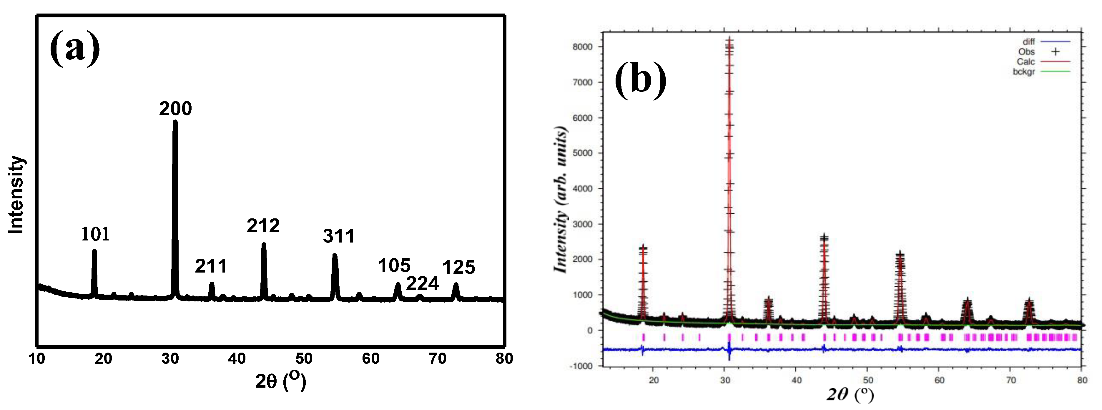
Figure 1a,b show the XRD plot of Sr
2CaTeO
6 and the refined data by the Rietveld refinement method. From refinement data, this compound formed in a single phase without any secondary phase(s) present with reliabilities (
χ2) of 1.15, which shows the very reliable refinement result as per the literature review. The single phase formed in a monoclinic structure of
P21/n symmetry. The obtained unit cell volume (
V) for the compound was 278.5 Å
3, with the lattice constants of 5.804, 5.838, and 8.219 Å, for
a,
b, and
c, respectively.
Table 1 shows the complete parameters that were obtained from the refinement. The refined structure parameters were comparable to the other report [
14].
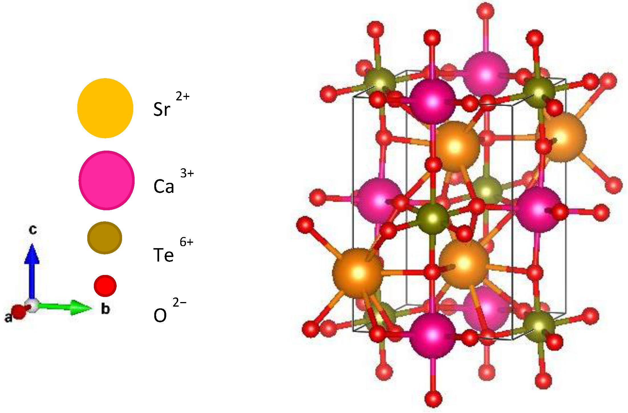
Figure 2 shows a refined structure of Sr
2CaTeO
6 from the
bc plane. It is clear that A-site cations (Sr
2+) are placed between B-site (Ca–O) and (Te–O) octahedral to strengthen the octahedral structure.
From
Table 1, there are different bond lengths existing within the B-site octahedral structure. A longer Ca–O bond compared to Te–O bond was attributed to the larger size and lower electronegativity Ca
2+ compared to Te
6+. Additionally, a stronger hexavalent hold of the Te–O bond could be the other factor that contributed to the aforementioned difference. The different bond lengths for each Te–O
1, Te–O
2, and Te–O
3 and Ca–O
1, Ca–O
2, and Ca–O
3 bonds indicate distortion in the octahedral shape and deviation from the equivalent bond lengths of the octahedral structure. Ca–O octahedral formed in elongate–like structure with the longest bond at Ca–O
3. Moreover, Te–O octahedral formed the compressed-like structure since the shortest bond was Te–O
3. The angle of 157.2° between Ca–O–Te can be referred to as the inclination between different octahedral structures. The deviation of the angle from 180° supported that structural distortion occurred in this compound. This value of bond angles indicates a higher inclination than other reported tellurium-based double perovskites [
19,
20]. The smaller value can be deduced due to the larger size of Ca
2+ at the B-site location in this compound and thus, decreasing the structural integrity. From
Figure 2, the different locations of Te
6+ in both compounds indicate that the B-site cations could fill any suitable locations. Nevertheless, the large difference in charge between Te
6+/Ca
2+ cations ensured that these cations’ locations were arranged periodically. Since there is a single type of A-site cations, hence, the formation of a layered arrangement of the cations can be withdrawn. Thus, any anion vacancies to accommodate this arrangement can be dismissed [
21]. However, since our solid-state method required the sintering at a temperature higher than 1000 °C, the evaporation of CaO chemical could take place [
22]. The oxygen vacancy in this sample was determined approximately to
δ = 0.05 as per refinement.
In order to calculate the tolerance factor of the sample,
τ, we applied Equation (1) [
3]:
where
RA = radii of the A-site atom,
RB and
RB′ = the radii of the B-site atoms, and
RO = the radius of the oxygen atom in Å.
The calculated tolerance factor (
τ) of the compound was 0.921, which shows a deviation from the cubic structure. This value confirmed the distortion occurrence between A-site and B-site and hence, distorted the shape of octahedral structures in this material. The size of cations used for the calculation were 1.44 Å (Sr
2+) with coordination number (CN) of 12 and 1.00 Å (Ca
2+), 0.56 Å (Te
6+) and 1.40 Å (O
2−) with CN of 6 [
23]. The calculated tilting angle for the compound can be calculated by using Equation (2) [
24]:
where
θ is the average angle for the (Ca–O–Te) bond. This value indicated the distortion and supported the inclination angle between octahedral structures within the compound. Meanwhile, the crystallite size (
D) was calculated by using the Scherrer formula [
25]:
where
K is the constant value, which is 0.9;
β is the full width at half maximum (FWHM);
θ is the angle of XRD peaks; and
λ is the wavelength of XRD beam in nm [
26,
27]. Both the calculated tilting angle and crystallite size of this compound were 11.40° and 10.71 nm, respectively.
Table 1.
Obtained space symmetry, parameters of lattice, V, angles of bonds, lengths of bond, and fit goodness from Rietveld refinement with calculated ϕ, τ, and D in Sr2CaTeO6.
Table 1.
Obtained space symmetry, parameters of lattice, V, angles of bonds, lengths of bond, and fit goodness from Rietveld refinement with calculated ϕ, τ, and D in Sr2CaTeO6.
| Lattice Parameters | Bond Lengths (Ǻ) |
|---|
| Space Symmetry | P21/n |
|---|
| a (Å) | 5.804 (2) | Ca-O1 (x 2) | 2.058 (9) |
| B (Å) | 5.838 (7) | Ca-O2 (x 2) | 2.199 (8) |
| c (Å) | 8.219 (4) | Ca-O3 (x 2) | 2.258 (12) |
| α | 90.00° | Ave. < Ca-O > | 2.172 (10) |
| ß | 90.21° | Te-O1 (x 2) | 1.992 (8) |
| γ | 90.00° | Te-O2 (x 2) | 2.194 (8) |
| Unit cell volume, V (Å3) | Te-O3 (x 2) | 1.899 (10) |
| 278.5 | Ave. < Te-O > | 2.028 (9) |
| Tilting angle, Φ | Ave. < Sr-Sr > | 4.119 (11) |
| 11.40° | Bond angles (°) |
| Fit Goodness |
| χ2 | 1.150 |
| Rp (%) | 4.9 | Ca-O1-Te | 158.1 (1) |
| Rwp (%) | 6.4 | Ca-O2-Te | 150.9 (1) |
| Crystallite size, D | Ca-O3-Te | 162.5 (1) |
| 10.71 nm | Aver. < Ca-O-Te > | 157.2 (1) |
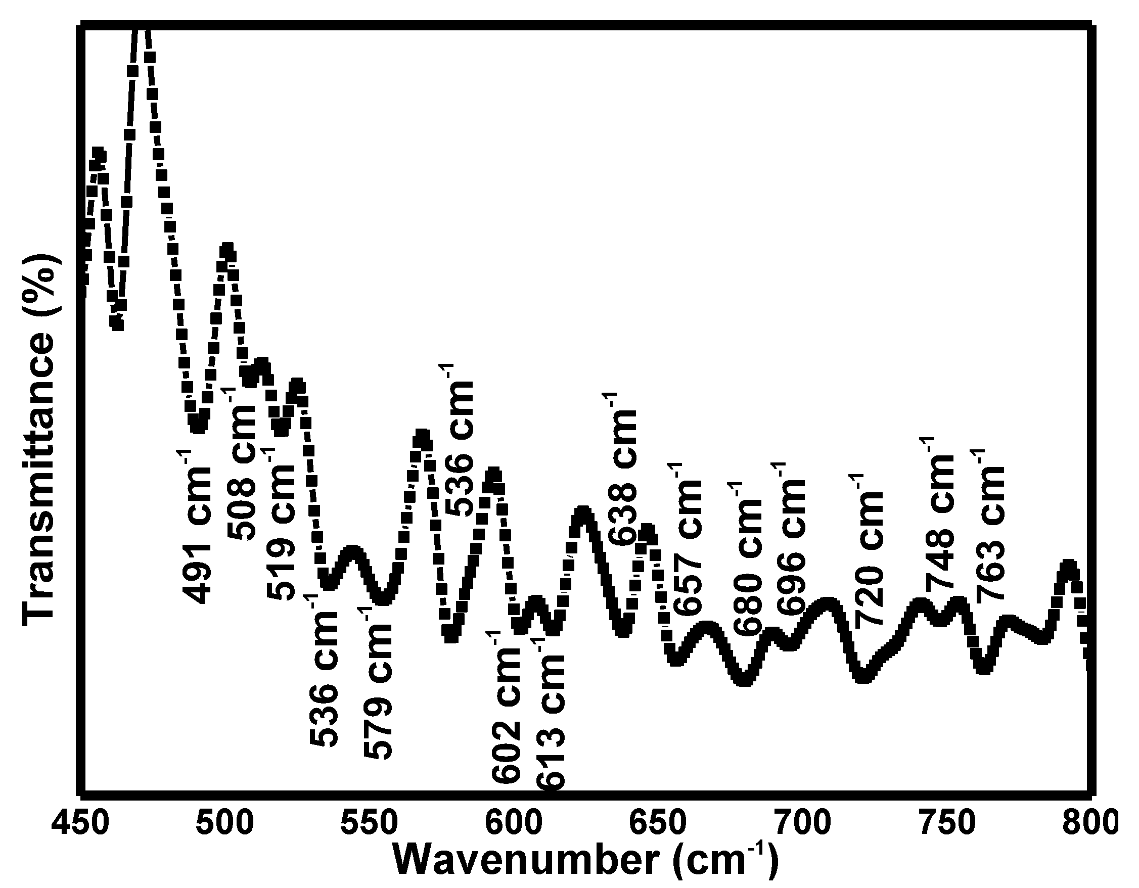
Figure 3 illustrates the FTIR spectrum of the Sr
2CaTeO
6 compound. Some important peaks were present in this spectrum. Peaks at 554 cm
−1 correlated with Ca–O bond stretching vibrations in octahedral structures [
28]. The emergence of medium peaks at 491, 508, 519 and 536 cm
−1 can be detected and be assigned to antisymmetric stretching vibrations (
v1) of Te–O bonds in the octahedral structures. At the same time, strong peaks at 555, 579, 602, 613, 638, 657, 680, 696, 720, 748, and 763 cm
−1 were clear and can be related to the symmetric stretching vibration (
v2) of the Te–O bonds [
29,
30,
31,
32,
33,
34]. These peaks’ existence proved the formation of Ca/Te–O bonds in this sample.
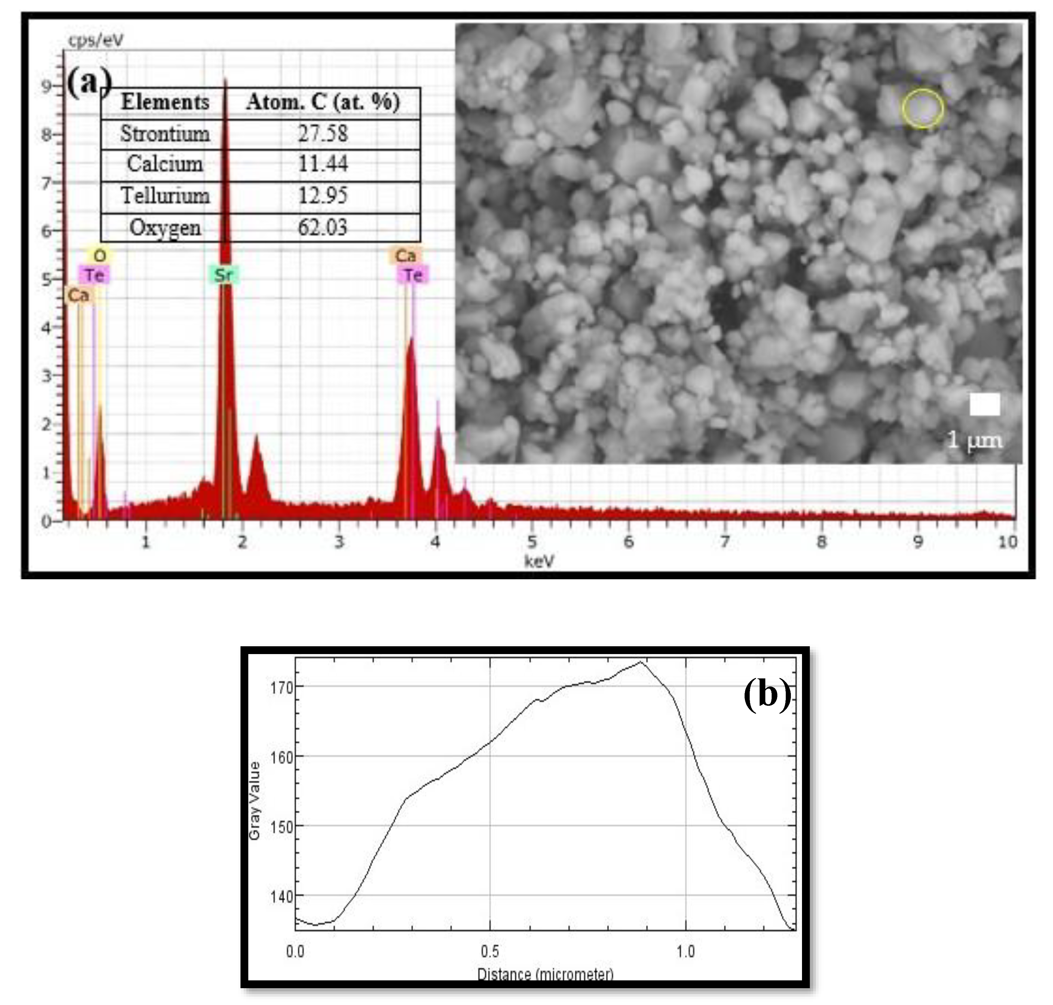
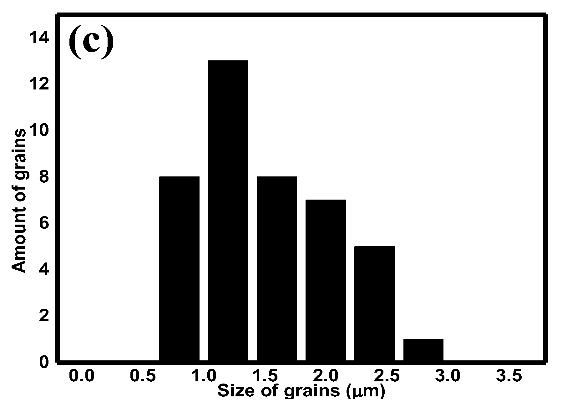
Figure 4a exhibits the morphology of the Sr
2CaTeO
6 compound. The formation of agglomerated grains with almost the same shape and size distribution as most grains was clear. The agglomerated particles in this compound were most probably due to the fast nucleation rate of grains, which was caused by high temperatures of calcination and sintering. Thus, this caused the grains to become accumulated since there was not enough duration for the grains to separate well from each other [
35]. The formation of grains can be confirmed in
Figure 4b, where the shape of the top cross-section of a grain (marked with a yellow circle in
Figure 4a) formed a hill shape. The obtained grain size distributions are displayed in
Figure 4c. The measured distribution grain sizes were within the range of 0.7–2.5 μm, with the majority of the grains’ sizes between 1.0 and 1.5 μm, while there were fewer grains with sizes greater than 2.0 μm. These sizes were relatively larger compared to other tellurium-based double perovskites [
36,
37]. EDX graph in
Figure 4a exhibits constituted elements in this sample, which confirms that these compounds contain elements of the prepared raw material composition, except Au, which originates from the coating in sample preparation for SEM characterisation. The sample’s density is 5.755 g cm
−3, as calculated by the Archimedes method.
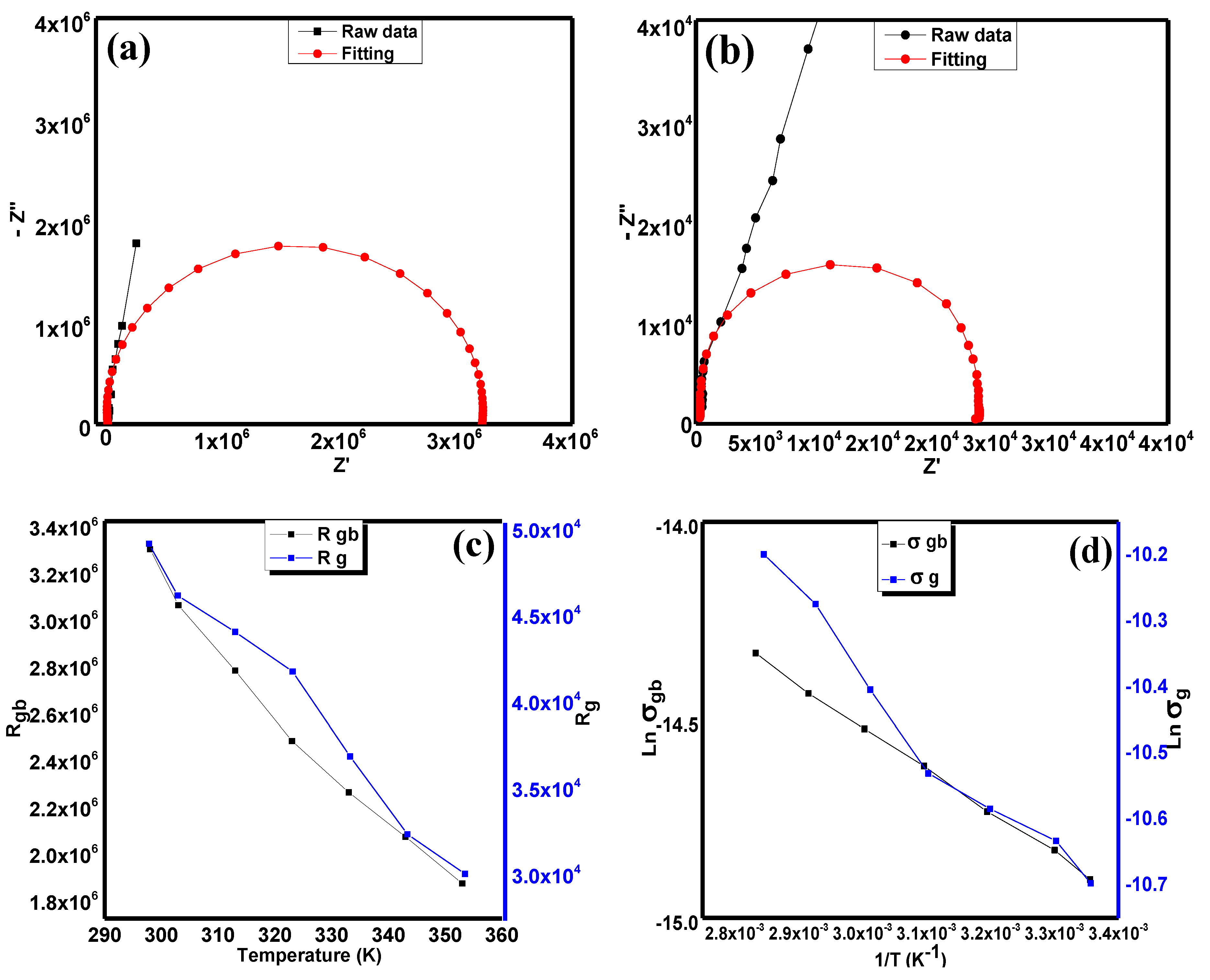
In order to obtain the basic idea of electrical conductivity in this compound, we utilised the Nyquist plot for this purpose.
Figure 5a,b exhibit the raw data and fittings of the Nyquist plot of Sr
2CaTeO
6 at both the full range of frequencies and high frequencies range.
Figure 5c shows the resistance obtained for two different regions, which are grain boundaries and grains in the compound.
Figure 5d exhibits the variation in DC conductivity in both grain boundaries and grain. Both of these plots show a decrease in resistance and DC conductivity against temperature and inverse of temperature, respectively.
From
Figure 5a, the almost straight line observed has proved that the resistive/capacitive behaviour of this compound is obvious. In addition, there is a small curve in the high frequencies range that indicates the presence of two different regions or mechanisms in this compound. In order to obtain the idea of basic behaviour and the resistance of grain boundaries and grains, the fitting and extrapolation of Nyquist data from low to high frequencies regions and at high frequencies only were carried out by using the Zview software. Based on these fittings, the Nyquist plot of Sr
2CaTeO
6 is suited to the grain and grain boundaries system and includes a constant phase element (CPE) and a resistor at each region. The presence of CPE indicates the non-ideal capacitive behaviour and possesses small electrical conductivity values. From the extrapolation from the fittings, the non-perfect semicircle shape at each fitting implies that the non-Debye impedance occurred within the compound. In order to obtain the resistance values at both grain boundaries and grains, we determined the
x-axis intercept from the extrapolation data. In
Figure 5c, it is clear that the values of grain boundaries and grain resistances decrease as the temperature is elevated.
The decreasing value of resistances in Sr
2CaTeO
6 from
Figure 5c indicates the negative temperature coefficient resistance (NTCR) behaviour, which is a characteristic typically possessed by a semiconductor. The value of grain resistances is much smaller by a factor of two compared to grain boundaries, which indicates the resistive property of grain boundaries that enclose the more conductive grains. In order to calculate the values of DC conductivity of this compound, Equation (4) was applied [
38]:
where
t = thickness of the sample, which is 2.05 mm;
R = resistance of grain boundaries/grain; and
A = area of electrodes attached to sample, which is 0.19 cm
2. From
Figure 5d, the DC conductivity at various temperatures obeyed the Arrhenius equation, as in Equation (5) [
38]:
where
Ea = activation energy in eV,
kB = Boltzmann constant, and
T = temperature in K. Hence, the obtained values of activation energy for grain boundaries and grain were 92 and 81 meV, respectively. The small difference between both energy values implies that the same charge carriers were involved for both grain boundaries and grain DC conduction. Moreover, these relatively small values of energy indicate the presence of free electrons in the grain or crystal lattice structure and near grain boundary regions. The presence of these free electrons most probably originated from the singly or doubly ionised oxygen vacancies, which could occur at high temperatures amidst the sintering process. The formed single or double ionised vacancies then produced the electrons by Equations (6) and (7) [
39]:
where
and
= single and double ionised oxygen vacancies, respectively.
In order to understand the ability of a compound to store static charge, it is crucial to undergo a dielectric study of a sample. The equation for the complex dielectric permittivity is given as in Equation (8) [
40]:
Figure 6a exhibits the plot of dielectric real permittivity,
ε′, with respect to frequencies from 50 Hz to 1 MHz in Sr
2CaTeO
6 compounds at different temperatures. The variation in
ε′ at each temperature shows the same shape and trend. At frequencies lower than 100 kHz, the huge drop in
ε′ can be observed before the slope of the drop decreases at higher frequencies until 1 MHz. At minimum and maximum frequencies, values of
ε′ in ambient temperature were 6800 and 3800, respectively. As the temperature increased, the
ε′ values increased accordingly.
Figure 6b illustrates the variation in
ε′ vs. temperatures at specific frequencies. Dispersion of
ε′ at higher temperature and the enhancement of
ε′ at different temperatures shows the temperature dependence behaviour of dielectric property in this compound. Moreover,
Figure 7c shows the tangent loss,
Tan δ, of the sample across frequencies at selected temperatures. The values of
Tan δ registered an increase in temperature with the presence of a peak at initial frequencies and around 100 kHz. At minimum frequency, the value of the loss was 0.25, while at maximum frequency, the loss registered at 0.05 at ambient temperature. At the second peak, the value of the loss was around 0.2 at the ambient temperature.
From
Figure 6a, the high values of
ε′ were probably due to the space charge polarization, where this effect was originated from the movement of charge carriers (heavy electrical dipoles) from oxygen vacancies defects within the grains or between the semiconducting grain and the more resistive grain boundaries, which then caused the heavy electrical dipoles to accumulate. Generally, all types of electrical polarisation, including dipolar, atomic, and electronics polarisations, were involved at initial frequencies and hence, contributed to the large total of dielectric real permittivity value in the compound. The large
ε′ values in this compound are much larger than reported tellurium based double perovskites with
AA′
BteO6 configuration such as SrLaLiTeO
6, SrBiLiTeO
6, and BaLaNaTeO
6 but with slightly larger dielectric loss [
11,
36,
37]. The difference in grain size between these compounds could provide the reasoning for the
ε′ value’s difference. Nevertheless, the sudden reduction in
ε′ at low frequencies was caused by the impotency of the aforementioned charges to follow the alternation of the electric field. Hence, only light electrical dipoles were able to complete the alternation with the external field until the maximum frequency. From
Figure 6b, the enhancement of
ε′ at every temperature indicates the non-relaxor type of polarisation in the compound and the absence of ferroelectricity transition characteristics within the studied temperature range. From both figures, the increase in polarisation with temperature indicated the conservation of total energy from thermal to kinetic energy, which aided dipoles polarisations. In this compound, the thermally activated polarisation at low frequencies can be related to space charge polarisation, while less temperature dependency of polarisation at higher frequencies can be related to lighter dipole polarisation. On the other hand, the stable increase in
ε′ over a wide range of frequencies at every temperature increment may suggest good polarisation, especially from ionic/atomic polarisation.
From
Figure 6c, the high values of
Tan δ at initial frequencies corresponded to the drop in
ε′ in the same frequency range as in
Figure 6a due to the movement of charge carriers within the grains or between the grain boundaries and grains. This movement would then cause the leakage current flow in the form of DC conduction during the alternation of the external field. This deduction is supported by the value (−1) of the gradient in log
ε″ vs. log
f plot in
Figure 6c. In addition, the inability of these electrical charges to effectively abide by the external field alternation could be a factor in assisting the high value of the loss. At low frequencies, the increased value of loss as temperature increases implied the increase in dynamic of the charge carriers and contributed to the enhancement of DC conductivity. The existence of peaks at higher frequencies at each temperature and their shifting towards the higher temperatures implied the presence of relaxation peaks at the respective frequencies. The presence of these peaks indicated the impotence of the charges to follow the alternation of the field due to AC conductivity or heat loss. The increase in the peak loss with temperature, however, indicated the increase in carriers’ movements, which strongly implies the presence of AC conductivity at high frequencies.
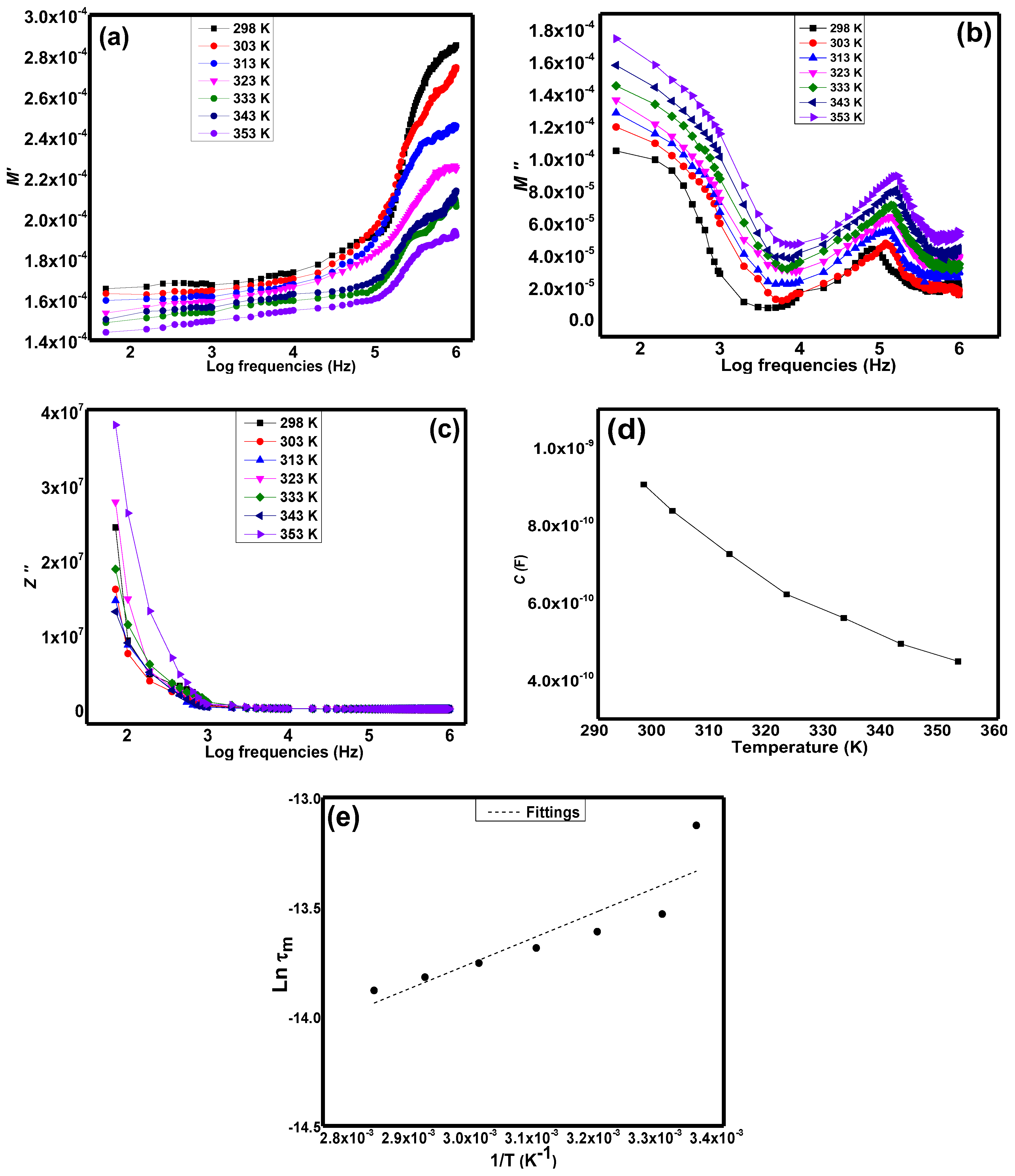
In order to obtain the full idea of the electrical contributions in the sample, the electrical modulus study can be carried out for this compound. The modulus formalism equation is the inverse of complex dielectric permittivity as Equation (9) [
40]:
Figure 7a illustrates the real electrical modulus,
M′ of Sr
2CaTeO
6 within frequencies of 50 Hz to 1 MHz. From this figure, there are two regions of variation, which are the low gradient plot at lower frequencies and the high gradient and dispersion plot at around 100 kHz and above.
Figure 7b shows the imaginary electrical modulus,
M″ of this compound. It can be observed that there is a presence of a peak at initial frequencies and at frequencies around 100 kHz.
Figure 7c shows the Bode plot of imaginary impedance,
Z″, at the same frequencies region. It can be seen that there are peaks present at frequencies lower than 50 Hz at each temperature.
Figure 7d shows the capacitance values in this compound at each temperature. The temperature-dependent capacitive property can be observed from this plot.
Figure 7e shows the relaxation times variation against the inverse of different temperatures graph. From this graph, the almost linear shape of variation can be seen across the temperature range.
From
Figure 7a, the small values of
M′ at initial frequencies can be related to the tendency for electrode effects to be suppressed and not contribute to the total electrical conductivity in this sample. In the low gradient region, it shows the almost plateau variation in
M′ and low electrical stiffness. This variation indicates that long-range conduction exists within the compound. On the other hand, the dispersed high slope region indicates the presence of short-range electrical conductivity at high frequencies, which means the localised conduction mechanisms of charge carriers exist within this frequency range. It is believed that carriers only move within their respective potential wells, led by the absence of the restoring force [
2]. With the presence of higher frequencies of an external field, the movement of charge carriers was merely conducted by the external field and hence, increased the electrical stiffness. The dispersion could also indicate the temperature-dependent relaxation process could take place within this frequency range. As the temperature elevated, the
M′ values decreased, which can be deduced that motions of charge carriers enhanced with temperatures. The shifting of the dispersion region towards lower frequencies as temperature elevated could indicate the short-range conduction took place.
From
Figure 7b, the primary peak indicates the presence of grain boundaries effect towards compound’s electrical characteristics. Nevertheless, the exact peak frequencies cannot be determined directly from this plot since lower frequencies are needed. The Bode plot from
Figure 7c supports that the grain boundary effects took place at lower frequencies. However, the plot does not show any presence of grain effect. The grain effect can be studied by analysing the
M″ plot. The peak at high frequencies in
Figure 7b refers to as grain effect towards the electrical property. This peak correlates well with the dispersion region in
M′ plot. As the temperature increased, the value of
M″ increased with the
M″max shifted towards the higher frequencies region; the shift supported
Tan δ results to indicate the relaxation frequencies region. The difference in
M″ values at each temperature suggests different capacitance at respective temperature and indicate a thermal effect on capacitance values. It can be seen that the values show a decrement from ambient temperature to 353 K. This can be understood since the dynamic of electrons is more progressive as temperature increases and hence, reducing the static charge storage and increasing the capacitive loss. This variation can be linked to dielectric real permittivity and dielectric loss in the sample shown in
Figure 6a,b. Meanwhile, the shifting of
M″max frequencies indicates the different relaxation times at respective temperatures by calculating the
ω−1. From
Figure 7e, the variation in relaxation peaks against the inverse in temperature followed the Arrhenius equation and could provide the activation energy of the relaxation process of electrical conductivity at specified frequencies. From this equation, the calculated activation energy,
Ea, obtained was 0.09 eV which was slightly different from DC conduction
Ea. The relaxation process from the
M” in this sample can presumably be due to AC conductivity. Hence, the difference between
Ea of DC and AC conductivities could indicate that different charge carriers were involved in both conductivities. Shorter relaxation times with temperature increases implied that more kinetic energy conversion contributes toward the dynamic of the charge carriers.
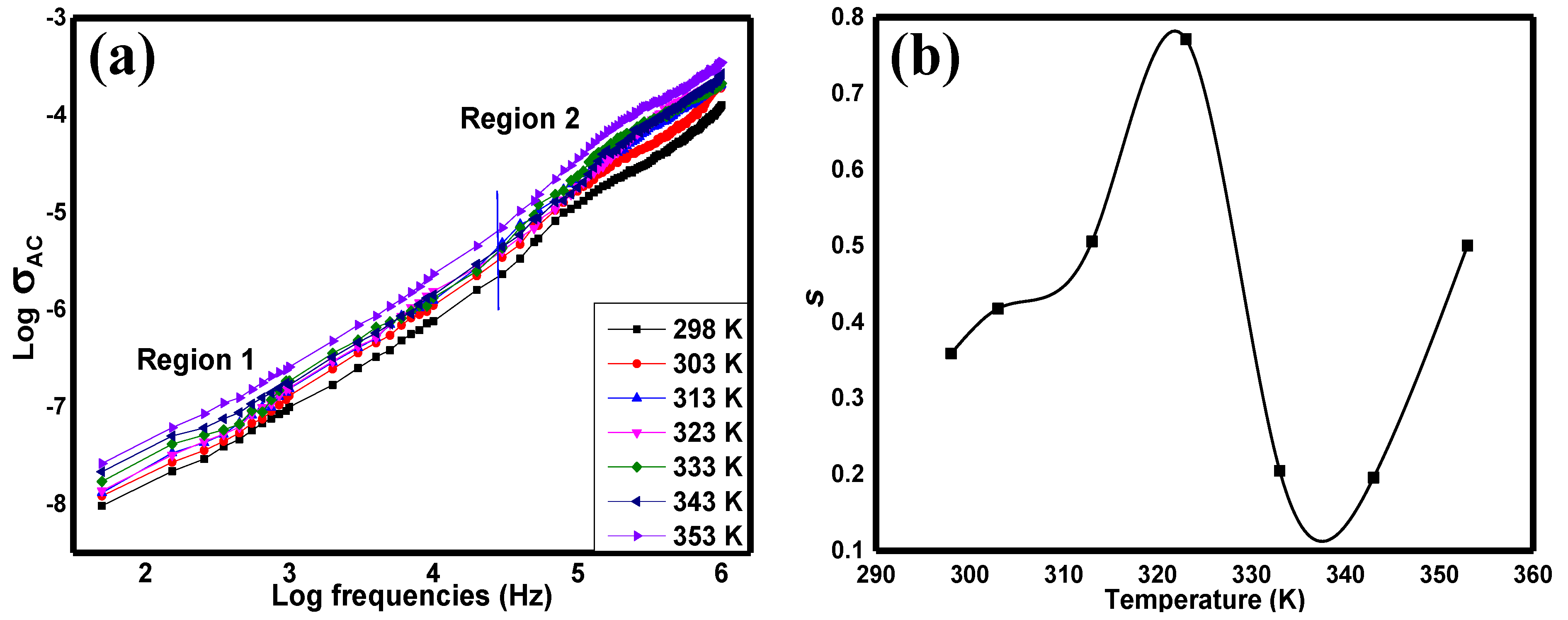
In order to understand the complete electrical conductivity of a sample, AC conductivity characterisation is needed to understand the electrical conductivity that takes place in the materials with the presence of the external electric field.
Figure 8a shows the AC conductivity of the Sr
2CaTeO
6 from the frequency of 50 Hz until 1 MHz. From this plot, there are regions of plateau and dispersion regions, separated by a solid blue line in the plot between 10 kHz and 100 kHz. The graph in
Figure 8b was plotted in order to further understand the AC conduction mechanism in Sr
2CaTeO
6. This graph shows the variation in s against different temperatures. The value of s can be obtained from the slope of log σ
AC vs. log f. According to this plot, the variation in s increases from ambient temperature until 323 K, decreases at 333 K, and increases back until 353 K, with the s values lying within the range of 0.1 to 0.8.
From
Figure 8a, in region 1, the plateau region could be related to the long-range DC conductivity at lower frequencies, while the dispersion region could be related to localised AC conductivity at higher frequencies. The increment of electrical conductivity from ambient temperature to 353 K correlates with the NTCR behaviour in grain boundaries and grain structures. The shape of this plot can be explained by the Jonscher Equation (10) [
40]:
where
A = pre-exponential constant, which indicates the polarisation strength, while
s = power-law exponent, which indicates the degree of carriers’ interactions with lattices structure. In the Jonscher equation,
σDC is related to DC conductivity, while
Aωs is related to AC conductivity.
Mechanisms that are commonly utilised to elucidate the AC conductivity properties of perovskites related to the variation in
s at different temperatures. For instance, variable range hopping (VRH), small polaron hopping (SPH), quantum mechanical tunnelling (QMT), non-overlapping small polaron tunnelling (NSPT), and overlapping large polaron tunnelling (OLPT) mechanisms [
18,
41,
42,
43,
44,
45,
46]. According to the pattern in
Figure 8b, a variation in
s values from 298 K to 323 K could be linked to NSPT or SPH. However, NSPT could be the most suited model since the
Ea from
M″, which were due to AC conductivity, is comparable to other double perovskites, as reported before [
43]. Furthermore, the variation in
s values from 323 K to 353K is in accordance with the variation in the OLPT model.
The AC conductivity of the NSPT model is given by the Equation (11) [
43]:
where
= the density of the localised state,
represents Boltzmann’s constant,
= the absolute temperature in K, and
= the tunnelling length at frequency
.
The
can be elaborated as in Equation (12) [
43]:
where
α−1 = spatial extension of the polaron,
τo = relaxation times in s, and
Wm = polaron hopping energy in eV.
The frequency exponent,
s, predicted by this model is given by the Expression (13) [
43]:
whereas the AC conductivity for the OLPT model is given by Equation (14) [
46,
47]:
where
= decay parameter for the localised wave function and
= the polaron radius.
The frequency exponent,
s, predicted by this model is given by the Expression (15) [
46]:
Charge carriers in the sample probably originated from electrons due to oxygen vacancies, which transform into polarons due to their movement in the deformed lattice of the sample when induced polarisation follows the electrons. In the case of small polarons, the size of the polarons was smaller than the lattice constant of the compound. Meanwhile, the size of polarons was greater than the lattice constant in large polarons formations. The large polarons that formed with shallow bound states were attributed to Coulomb interaction between charge carriers and polarisable lattice. Both types of charge carriers were able to move across sites with potential energy well by tunnelling mechanisms between oxygen vacancies [
48]. In both NSPT and OLPT models, the polaron wells overlapped at two sites and hence, reducing the polaron energy to travel across the sites.
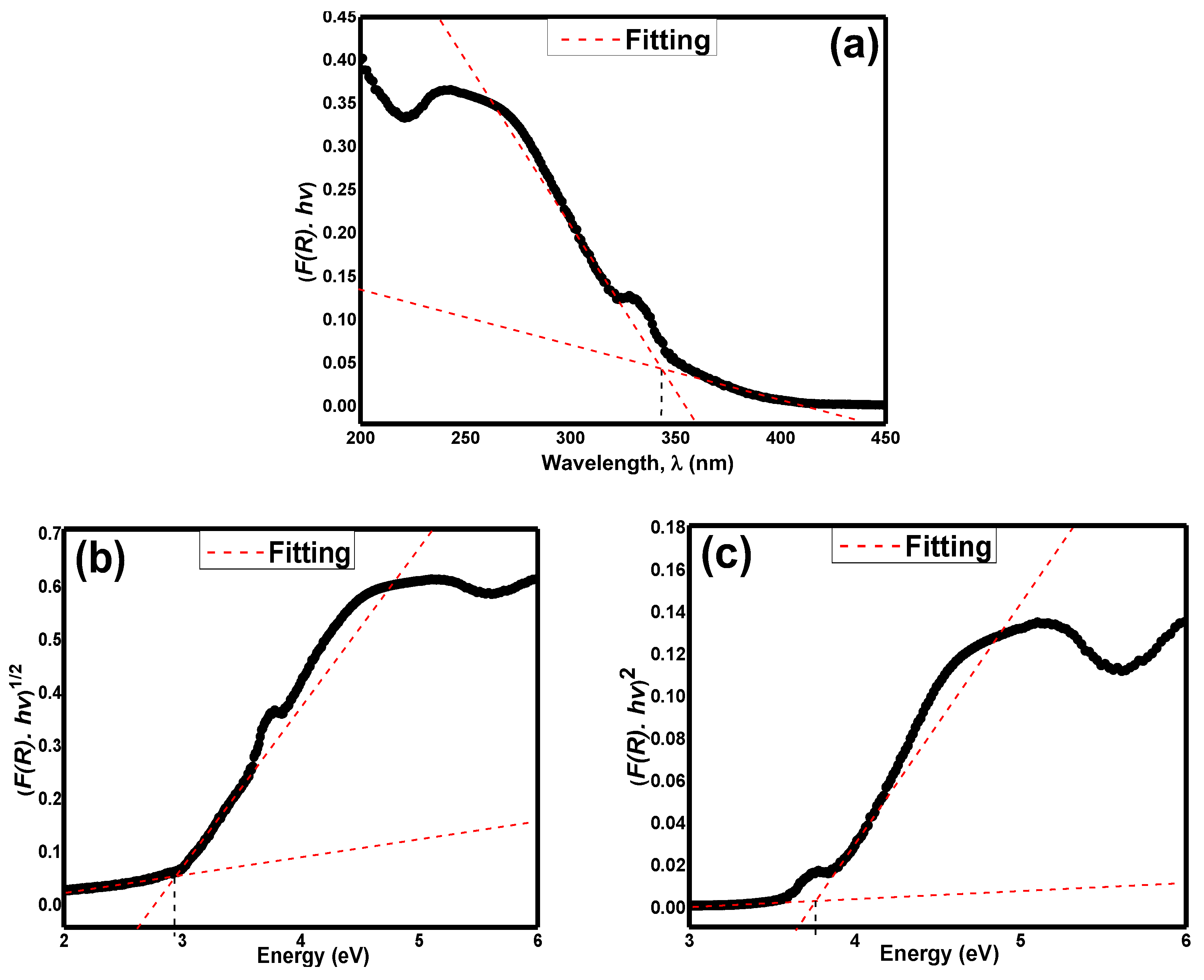
Towards understanding the basic optical property of this material, it is important to analyse the UV–vis characterisation study.
Figure 9a exhibits the UV–vis absorption plot of Sr
2CaTeO
6. The plot was calculated from Kubelka–Munk equation as in Equation (16) [
47]:
where
R = diffuse reflectance of compounds.
Figure 9b,c shows the Tauc plots that utilised Equation (17):
where
hv = photon energy,
A = proportional constant, and
Eopt = energy of optical bandgap. Meanwhile, the values of
n can vary based on the transition type in a material, where
n = 1/2 indicates the direct allowed transition,
n = 2 indicates the indirect allowed transition,
n = 3/2 indicates the direct forbidden transition, and
n = 3 indicates the indirect forbidden transition [
47].
From
Figure 9a, the value of the absorption point is around 343.2 nm. Hence, the calculated value of
Eopt from this absorption plot is 3.61 eV. Meanwhile,
Figure 9b utilised the indirect allowed transition of electrons. From this figure, the extrapolated value of
Eopt is 2.92 eV. From
Figure 9c, the fitting and extrapolation of
Eopt applied the direct allowed transition of electrons. The value of
Eopt measured from this transition is 3.75 eV, which showed much larger energy needed for the transition of electrons from the highest valence band to the lowest conduction band, despite only photons being involved in this kind of transition.
The indirect allowed type of transition was considered because of the presence of the hump in the absorption plot before the values become quenched at a higher wavelength. This could indicate that the indirect allowed transition was involved in this compound with the inclusion of photons and phonons movements. The obtained value of
Eopt was comparable to the result from other reports [
41]. However, based on the Kubelka–Munk absorption wavelength, the direct allowed
Eopt can be favoured as well as
Eopt values from both Kubelka–Munk and allowed direct transition is comparable. Furthermore, the shape of the plots is more similar despite their shape being inverse to each other. Values from all plots indicate the semiconductor range of
Eopt in this compound. However, the
Eopt values obtained from direct allowed transition lie in a wide semiconductor band gap range. Compared to other tellurium-based double perovskites, the
Eopt of allowed indirect transition in this compound showed a much smaller value [
37,
47] despite more distortion within this compound. This smaller
Eopt could be linked to the crystallite size difference between the compounds nonetheless [
49]. Additionally, the smaller
Eopt in this compound could be related to possible minor oxygen vacancies existence that could involve in the formation of the energy level of impurities within the sample band gap or lifted the Fermi energy and thus, reducing the
Eopt value [
50]. However, as per refinement analysis, the basic lattice structure of the compound was well-formed. Furthermore, the caution measure was taken by using a slow cooling rate to maintain the stoichiometry of the compound. Hence, it can be deduced that the oxygen vacancies formed are very minimal and should not affect the
Eopt majorly. The absorbance spectra of Sr
2CaTeO
6 and its semiconducting range of
Eopt indicate its potential to be utilised in UV range applications such as ultraviolet detector devices.


