Review

A Review of Nanocrystalline Film Thermoelectrics on Lead Chalcogenide Semiconductors: Progress and Application

1
Department of Materials Engineering, Ben-Gurion University of the Negev, Beer-Sheva 84105, Israel
2
V.E. Lashkaryov Institute of Semiconductor Physics, National Academy of Sciences of Ukraine, 03028 Kyiv, Ukraine
3
Department of Computer Engineering and Electronics, Vasyl Stefanyk Precarpathian National University, 76018 Ivano-Frankivsk, Ukraine
4
School of Electrical and Computer Engineering, Ben-Gurion University of the Negev, Beer-Sheva 84105, Israel
*
Authors to whom correspondence should be addressed.
Energies 2023, 16(9), 3774; https://doi.org/10.3390/en16093774
Submission received: 30 March 2023 / Revised: 24 April 2023 / Accepted: 25 April 2023 / Published: 28 April 2023
(This article belongs to the Special Issue Theory and Applications of Thermoelectric Materials and Devices)

Abstract

:
Submicron-structured films of thermoelectric materials, exhibiting an improved thermoelectric figure of merit, are reviewed, including methods of fabrication and characterization. The review emphasizes the beneficial role of the grain boundaries in polycrystalline films. The enhanced Seebeck coefficient of lead chalcogenide films is attributed to a potential relief that is built along the grain boundaries. It scatters charge carriers with low energy and does not affect carriers with higher energy. The model that accounts for the thermoelectric properties of the films is described and assessed experimentally. The application of a flexible thermoelectric device (module) based on the nanocrystalline film thermoelectric semiconductors as high sensitivity radiation detectors is suggested.

1. Introduction

Thermoelectric materials are used for solid-state refrigeration and energy conversion in bulk form. In recent years, nano-thermoelectrics have been investigated widely, with the goal of the efficiency optimization of the efficiency of TE devices [1,2,3,4,5]. Various methods including decomposition at solid-state synthesis [6] and preparation of nanopowders [7] are used for the preparation of nanostructured materials.
The enhanced performance (ZT > 1) of thermoelectrics with low-dimensional structures was reported by several groups, as recently reviewed by [1]. These improvements were mainly obtained by reduced phonon thermal conductivity. Another possibility that thin films may offer is the quantum confinement of electronic carriers. The present review discusses such a mechanism revealed in lead chalcogenide (PbTe, PbTe, PbS) semiconductor films.
The performance of the thermoelectric materials depends on a figure of merit Z or of dimensionless ZT, which is defined as [8]:
ZT = (S2σ/κ)T,
where S is the Seebeck coefficient of thermoelectric material (n- or p-type conductivity), σ and κ are their electrical and thermal conductivities, respectively, and T is the absolute temperature.
For the charge (electrons and holes) scattering on phonons, S is determined as [8]:
S = k B e 2 F 1 µ F 0 µ µ ,
where kB is the Boltzmann constant, e is the charge of electrons, Fi is the Fermi integrals, µ* is the reduced Fermi level.
The electrical conductivity σ of a semiconductor is given by the formula [8]:
σ = en(p)µnp),
Here n(p) is the electron (hole) carrier concentration, and µnp) is the charge carrier mobility.
The electron carrier concentration is given by:
n = 4 π ( 2 m n k B T ) 3 / 2 h 3 F 1 / 2 µ ,
Here m*e is the density of state (DOS) effective mass.
In the case of many (N) ellipsoids band-structure model [8]:
m e = N 2 / 3 ( m 1 m 2 m 3 ) 1 / 3 ,
where m1, m2, m3 are the effective mass components along the main ellipsoid axis.
The hole concentration is given by
p = 4 π 2 m p k B T 3 2 h 3 F 1 / 2 µ ,
where m*p is the density of state effective (DOS) mass of holes.
The charge mobility in a semiconductor with a simple parabolic band is given by [8]:
μ = e τ / m c ,
where τ is the relaxation time and m*c is the effective mass of carrier mobility [8].
For semiconductor (thermoelectric) materials, the thermal conductivity к has three partial components [8]:
k = k L + k e + k a ,
where kL is the lattice thermal conductivity, ke is the electronic thermal conductivity, and ka is the ambipolar thermal conductivity, which only appears at the intrinsic conduction area of semiconductor due to the diffusion of electron–hole pairs.
The lattice thermal conductivity kL is given by [8]:
k L = 1 3 C v ν 3 ,
where Cv is the specific heat at constant volume, and ν is the phonon velocity.
The electronic thermal conductivity ke is given by [8]:
k e = L 0 σ T ,
where L0 is a Lorenz number. For the acoustic phonons, the scattering Lorenz number is given by [8]:
L o = ( k o / e ) [ ( 3 F 2 ( m ) / F o ( m ) ) ( 2 F 1 ( m ) / F 2 ( m ) ) ] ,
The Seebeck coefficient S decreases with the increase in charge carriers’ concentration n(p), and in a metal with charge carriers concentration, n~1022 cm−3 S is close to zero. At the same time, electrical conductivity σ increases with increasing the charge carriers concentration n(p). Therefore, the dependence of the product S2σ on Fermi level EF is bell-shaped. The maximum of S2σ is achieved when EF~EC—the bottom of the conduction band in n-type semiconductor or EF~EV—the top of the valence band in the p-type semiconductor. In this case, the value of the Seebeck coefficient Sn ≈ −180 μV/K for the n-type and Sp ≈ 180 μV/K for the p-type, respectively, for the charge carriers’ concentration n(p)~3 × 1018 cm−3 [9]. For this carrier concentration, the thermal conductivity κ is determined mainly by lattice thermal conductivity κL [8,9]. For the optimal charge carrier concentration (reduced Fermi level μ* ≈ 0), the figure of merit Z is determined by only three parameters [8]:
Z m n 3 / 2 ( µ / k L ) ,
Nanostructured film materials have become a topic of intense interest in recent years, arising from their potential applications in the field of thermoelectric power conversion. The authors have systematized and generalized the methods and investigation results for nanostructured films of lead chalcogenide semiconductors for thermoelectric applications. Factors that influence the figure of merit Z include the barrier structure on grain boundaries in such films and the phonon scattering on nanograin boundaries. The practical application of the thermoelectric device as a thermal detector of radiation is suggested based on nanocrystalline-film materials.

2. Materials and Methods

Various methods including decomposition at solid-state synthesis [6] and preparation of nanopowders [7] are used for the preparation of nanostructured materials. In this work, the flash evaporation technology method, first developed by Prof. Z. Dashevsky for Bi2Te3 based compounds [10,11], was used for the preparation of the lead chalcogenides (PbTe, PbTe, PbS) semiconductor films [12,13,14,15,16,17,18,19,20,21,22,23,24,25]. The setup for the film preparation is presented in Figure 1 [11]. The flash evaporation method provides an opportunity to deposit the same composition of the evaporated PbTe, PbTe and PbS powder with a small dopant amount (for the n-type materials it is 0.1 to 1 at % of I or In, and for the p-type ones it is 0.1 to 1 at % of Na). The films were evaporated on a thin polyimide substrate with a thickness of ~10 µm. The benefits of the polyimide material are a low thermal conductivity (of ~3.5 × 10⁻³ Wcm−1K−1) and mechanical flexibility [26]. The temperature of the substrate during the film preparation ranged from T = 100 K (cooling of the substrate by liquid nitrogen during the evaporation) up to Ts = 573 K (by heating the substrate). The evaporation speed was ve = 0.1 mm/min. The film thickness was determined by the deposition time and was measured using a micro interferometer MII-4 with an accuracy of 0.1 mm. After the evaporation process, certain films were annealed in the same chamber at Tt = 673 K for 0.5 h in an oxygen atmosphere at the pressure p = 0.9 atm. It is known [27,28,29,30,31] that under an oxygen atmosphere an oxide barrier forms which prevents nanocrystal agglomeration and growth, thus keeping a high grain boundary area, and this may affect the position of the Fermi level.
The method of X-ray structural analyses of films was described in [18]. SEM images were taken with a Quanta 200 environmental scanning electron microscope (HRSEM) equipped with energy dispersive X-ray spectroscopy.
For the investigation of the transport properties of thin films over a wide temperature range of 10 K–300 K, including the Seebeck coefficient S (6% accuracy), the electrical conductivity σ (6% accuracy), the Hall coefficient RH (8% accuracy), and the Nernst coefficient QN (12% accuracy), a setup presented in Figure 2 was used [32]. The measurement of RH was carried out in permanent magnetic fields up to 2 T, and the reported results are the average of measurements in two directions of the electrical and magnetic fields. The accuracy of the temperature measurement was 0.1–0.2 K, and of the magnetic field it was ±3%.
The thermal diffusivity of thin films at the 300–350 K temperature range was measured in a setup presented in [32,33]. It used the method of dynamic gratings (Figure 3). Thermal gratings were generated by a 20 ns pulsed laser radiation with a wavelength of 532 nm and recorded by a 635 nm continuous laser radiation. By analysis of the kinetics of the diffraction signal, the lifetime of the recorded thermal gratings was determined. The accuracy of thermal diffusivity measurements was 10%. The total thermal conductivity of thin films was calculated from the equation [34]:
κ = α ρ c p ,
where α is the thermal diffusivity, ρ is the single crystal density, and cp was calculated within the Dulong-Petit limit.

3. Results and Discussion

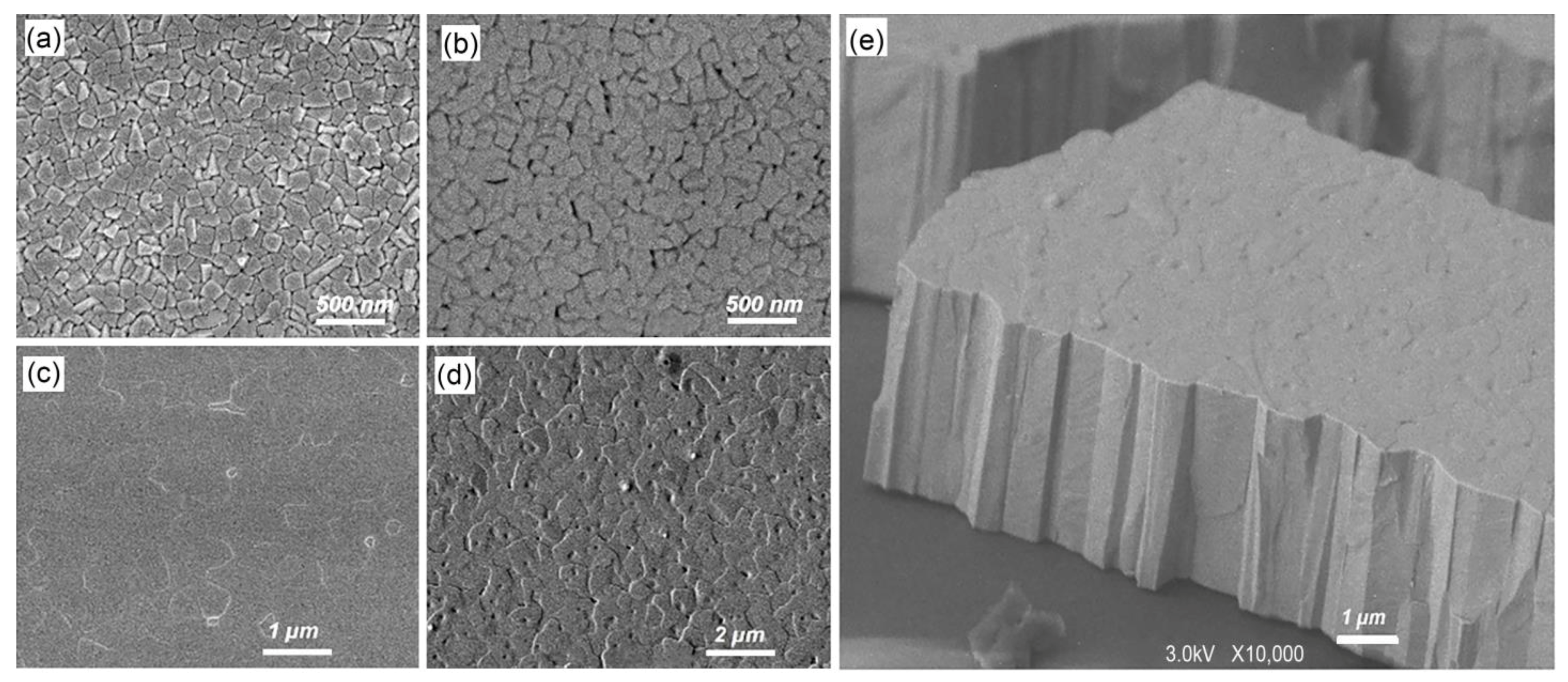
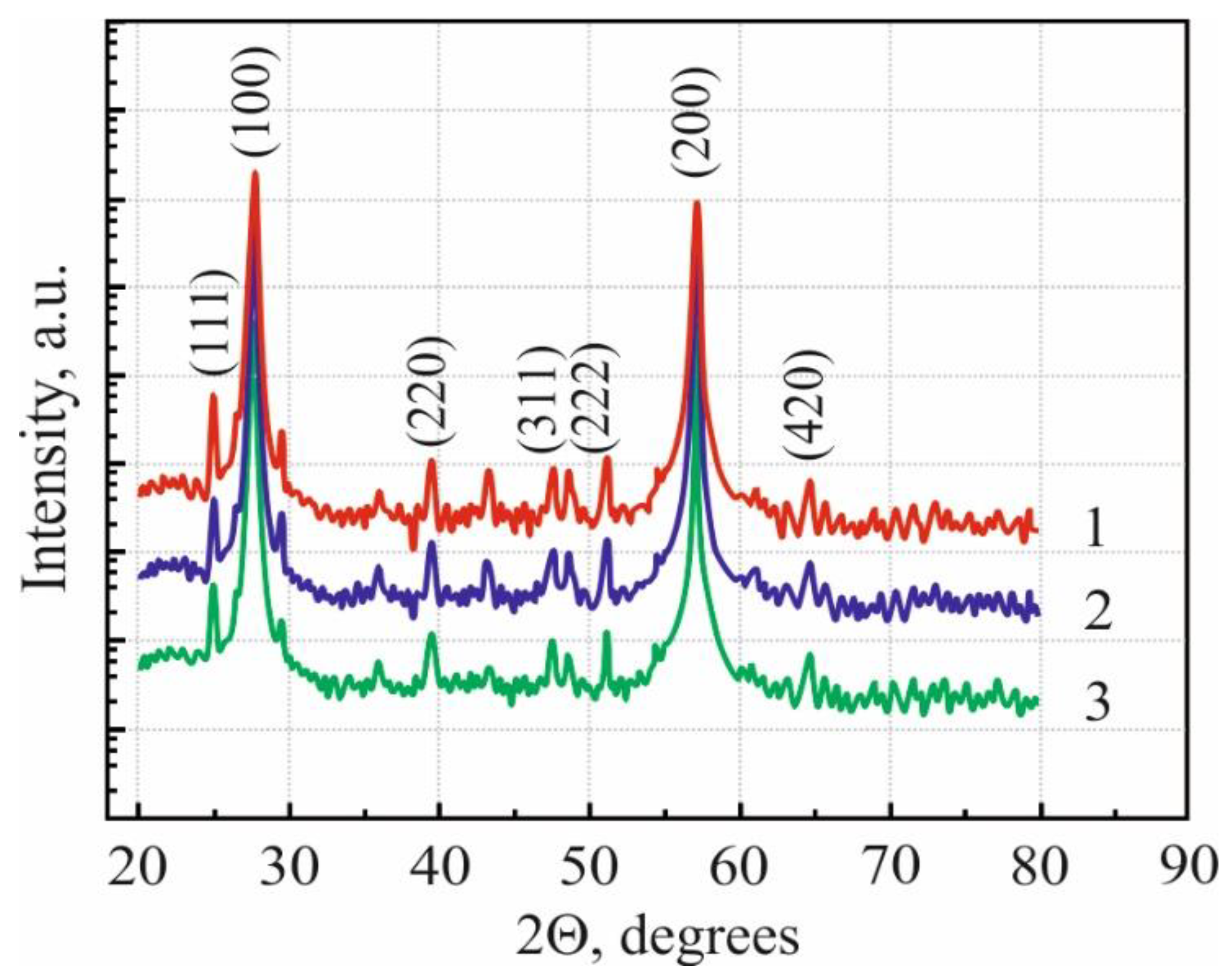
3.1. Structure Properties

Figure 4 presents an SEM image of as-grown PbTe films on an amorphous polyimide substrate at different substrate temperatures. The grain size is found to increase with the increase in temperature. The average grain size is 100 ± 20 nm at Ts = 100 K, 250 ± 40 nm at Ts = 300 K, and 400 ± 50 nm at Ts = 500 K. As-grown polycrystalline PbTe films on an amorphous substrate have a columnar structure (Figure 4e).
The XRD patterns of the grown PbTe films at different substrate temperatures Ts are presented in Figure 5. The main peak corresponding to (100) planes is similar to a single crystal with a cubic NaCl structure. Other XRD peaks with small intensities correspond to the (311) and (111) planes of PbTe.

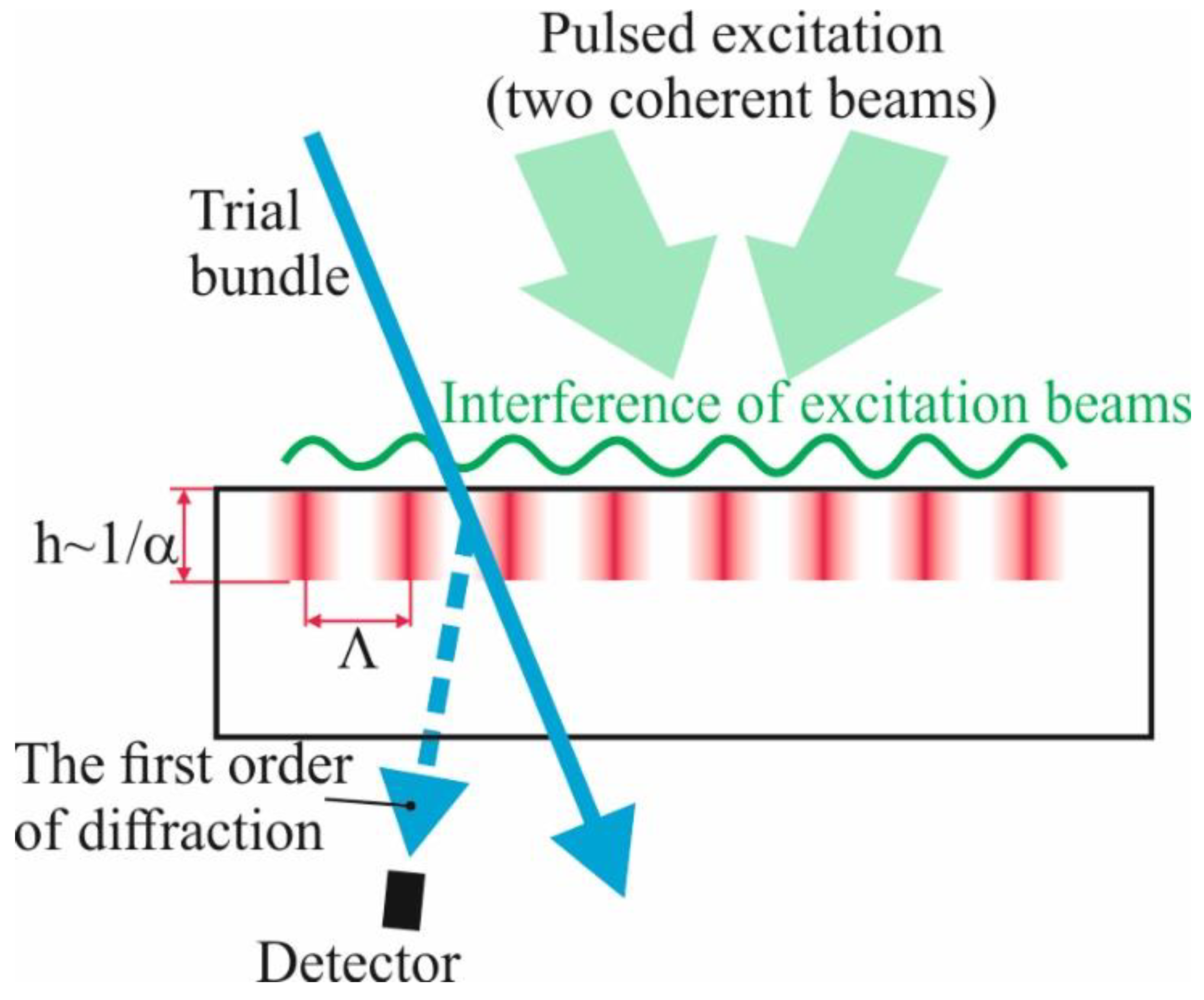
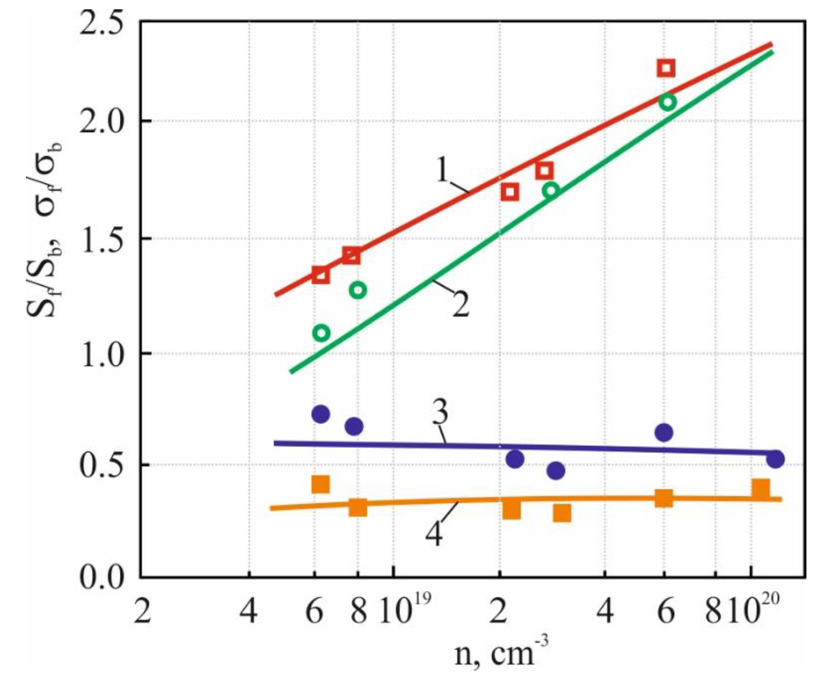
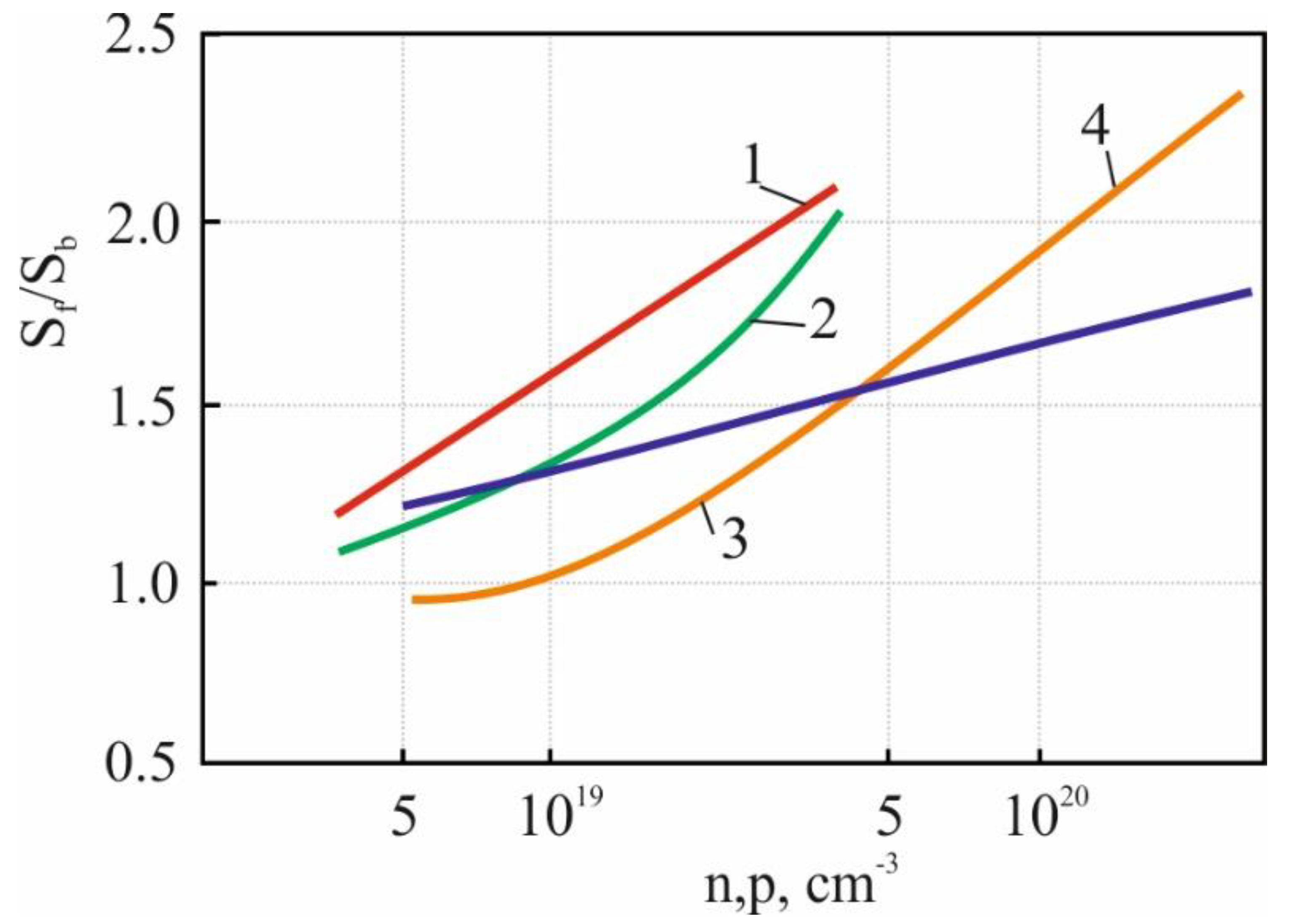
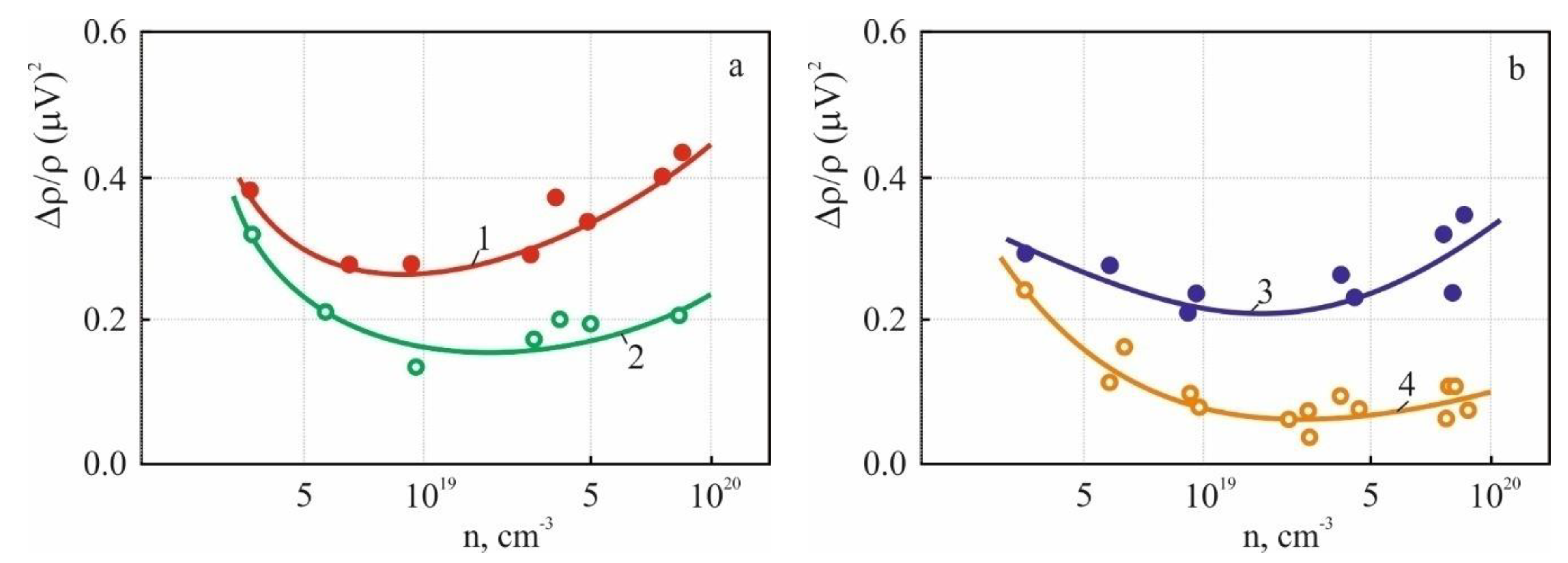
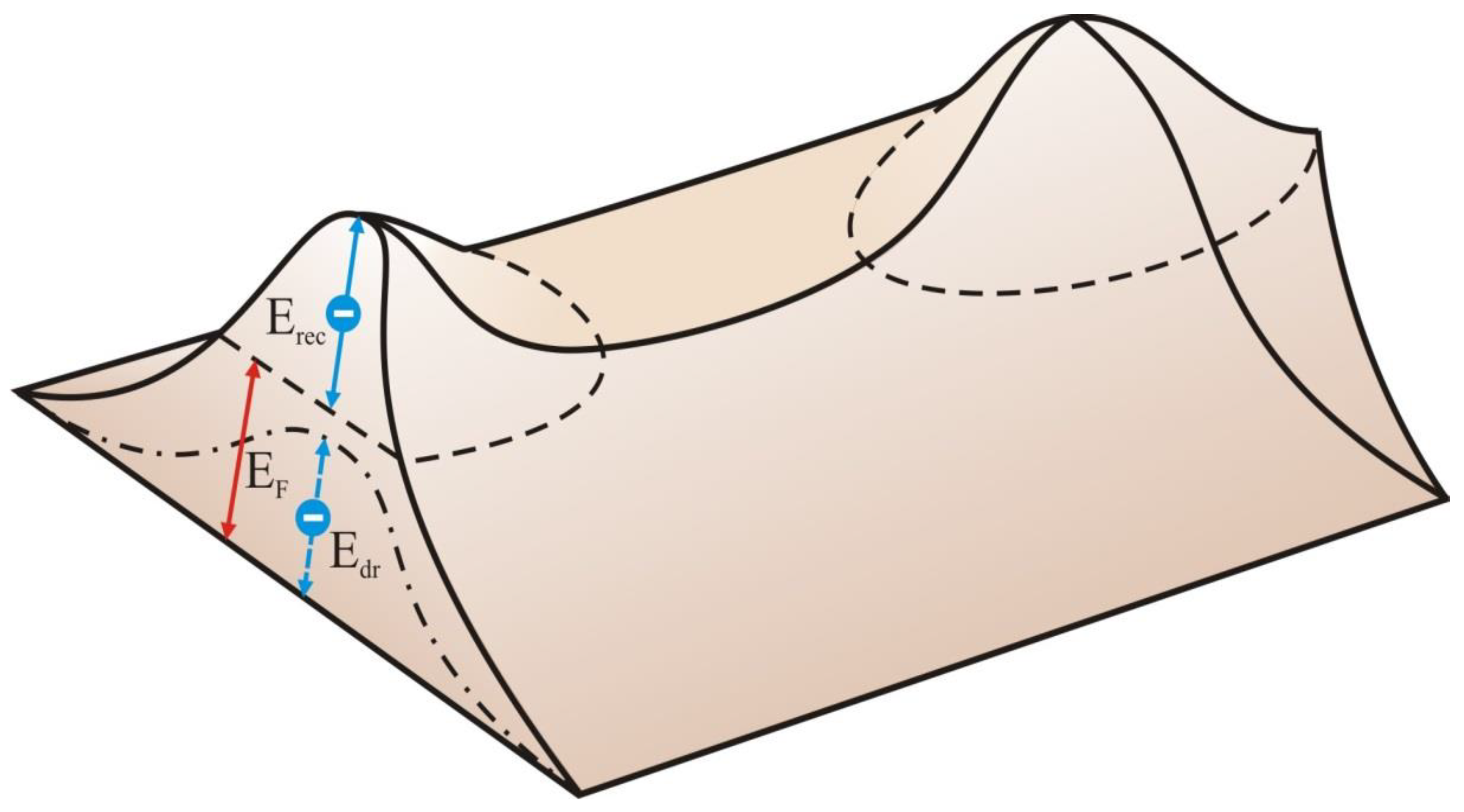
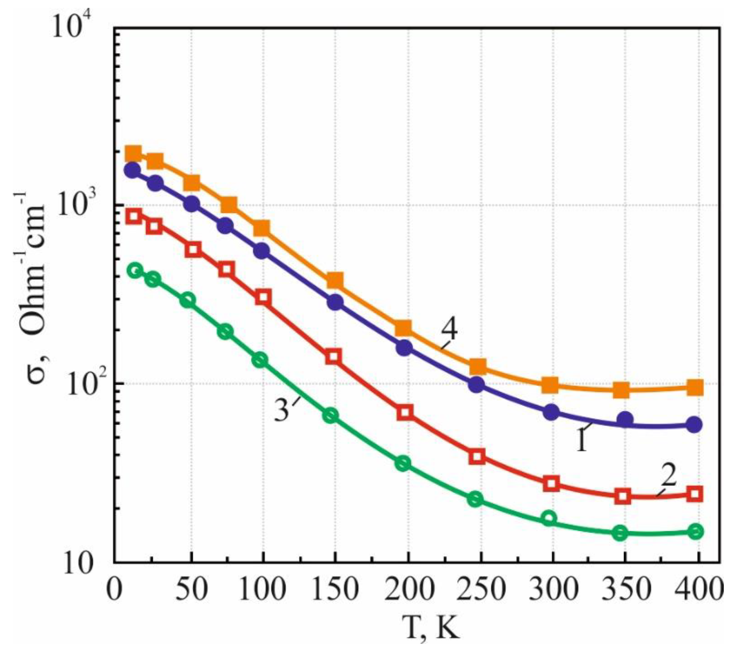
3.2. The Features of Charge-Carriers Scattering in Nano (Submicron)-Grained Films of Lead Chalcogenides

The charge scattering mechanism was studied in the n-PbTe films on a polyimide substrate with a grain size of ~400 nm. σ, RH, and the S, and QN coefficients were investigated over the 80 K–300 K temperature range. The electron concentration varied in the range of 1018 to 1020 cm−3. A comparison of the properties, obtained for the films with a thickness of d~1 μm with data for the bulk n-type PbTe single crystals, was reported in [32,35,36,37]. The following features of the films were observed: a decrease in electrical conductivity (electron mobility) by about 0.6 times at 300 K and slightly more at 100 K for all carrier concentrations (Figure 6), and an increase in S that is greater the higher the carrier concentration (more than two times at the carrier concentration n > 1020 cm−3). This implies a decrease by 1.7–2 times of an absolute value for the dimensionless parameter (e/kB) (QN/|RH|σ).
The calculation of the density of a state’s effective mass m*d and scattering parameter r by measuring of the four transport coefficients σ, S, RH, QN and using Equations (14) and (15) was made by the equations [32,38]:
m*d = (3n/π)2/3(e2/kB2T) (SQN/|RH|σ),
r = (QN−/|RH|σ/(SQN/|RH|σ),
where ℏ is the reduced Planck constant. The electron mean free path is l = l0Er, where l0 is a constant, and E is the electron energy.
The results of the calculation of m*d from Equation (14) were only slightly different from those obtained for bulk single crystals of PbTe [9]. This result, as well as the results of measurements of the optical band gap in the same films [20], made it possible to exclude changes in the band parameters in PbTe films. The observed differences between S and QN of PbTe films and of the bulk single crystals can be related to the appearance of an additional scattering mechanism. A two- to three-fold decrease in electron mobility indicates that the relative contribution of this mechanism is approximately the same as the contribution of phonon scattering to the electron mobility. Phonon scattering dominates the bulk PbTe properties over the 100–300 K temperature range. The increase in |S| and a decrease in |Q| indicate a higher scattering parameter r due to the additional mechanism. Using the experimental values of σ, RH, S, QN, the effective scattering parameter, characterizing the mixed scattering, ref was determined by the formula from [10]:
r e f µ = 3 2 S S Q N 1 + 3 d   l n   m d d   l n   n ,
After that, the parameter only characterizing the additional scattering, r2 was calculated. This was carried out by assuming strongly degenerate electron gas,
µ = µ 1 µ 2 / ( µ 1 + µ 2 ) ,
r e f = µ 2 r 1 + µ 1 r 2 / µ 1 + µ 2 ,
Here, μ is the electron mobility in the PbTe film, and μ1 and r1 are the electron mobility and scattering parameter, for the PbTe single crystal (the scattering occurs due to phonons [29]), respectively. The results of the calculation for temperature T = 120 K are listed in Table 1.
The mobility μ2 depends weakly on temperature, consistent with the assumption of scattering by defects. Despite the large values of r2, indicating a strong increase in the relaxation time with carrier energy, the mobility μ2 decreases significantly with an increase in the Fermi energy µ*. This is possible if the concentration of scattering defects increases with increasing electron concentration, or if the power of the scattering potential of each defect increases with increasing Fermi energy. Therefore, the additional scattering mechanism can be associated with intergrain boundaries. This assumption is supplemented by the following considerations. Electronic states can be localized at the boundaries of the grains, the filling of which charge the boundaries, creating potential barriers on them that scatter electrons. With increasing Fermi energy, the filling of these states, their charge, and the height of the potential barrier increase, which thus follows the Fermi level. If the barrier height is Eb » µ*, then such a barrier effectively dissipates carriers with energy less than the Fermi energy and weaker with higher energy, thereby creating a strong dispersion of the free path near the Fermi level. This gives rise to a large scattering parameter r2 and ref.
A scattering model on two-dimensional potential barriers is of considerable interest from the point of view of increasing the thermoelectric figure of merit Z. Consider, for example, a metal—a material with high electrical conductivity and low Seebeck coefficient. In the presence of highly selective barriers, electrons with energy lower than the Fermi energy scatter and practically do not contribute to charge transfer, while electrons with higher energy retain the same free path as in a defect-free crystal. In this case, the electrical conductivity, roughly speaking, would decrease by half. At the same time, the Seebeck coefficient would increase to a value of the order of 100–200 μV/K. At the same time, the specific power P = S2σ would significantly exceed the value currently achieved by the best thermoelectric semiconductor materials. For metals with k~ke and ZT » S2/L (L is the Lorentz number). At S » 100–200 μV/K and L~(2–3) (kB/e)2 thermoelectric figure of merit Z can be achieved, which is at the level of the best known semiconductors, or even higher than that. It is clear that such a model is idealized. Nevertheless, even stricter estimates have shown the reality of the increasing of Z, due to the scattering by two-dimensional potential barriers.
Studies of n- and p-type nano- and submicron-grained PbSe have shown the effect of a strong increase in the Seebeck coefficient S with a slight decrease in electron mobilityμ. Figure 7 presents an increase in Seebeck coefficient S for PbSe films compared to bulk single crystals. The m*d values determined from S, RH, σ and QN indicate the identity of the band parameters of the bulk single crystals and PbSe films. The value of the additional scattering parameter r2 calculated from (16) is greater than two. In such films, the crystalline grains grow from the substrate to the surface of the film (Figure 4e), i.e., the height of the crystalline grain is equal to the thickness of the film d. Films with a thickness d up to 2 mm were studied. The dimension size of the crystalline grains was 500 nm, as with n-type PbTe films.
In such a spatially anisotropic barrier structure, there should be a significant anisotropy of the coefficients describing the transport phenomena in the directions perpendicular and parallel to the plane of the film. However, due to the small thickness of the sample, it was difficult to experimentally measure the electric field, current, and temperature gradient in the direction perpendicular to the plane of the film. Therefore, the magnetoresistance was measured at two orientations of the magnetic field (perpendicular and parallel to the surface of the film). PbSe was chosen among the lead chalcogenides, since its iso-energy ellipsoids are weakly elongated [29], so that the anisotropy associated with the multipole spectrum is weakly expressed and should not obscure the spatial-structural anisotropy.
The mobility in the films, determined by the dependence of the electrical conductivity on the magnetic field, turned out to be approximately three times less than in bulk PbSe samples. When measuring the magnetoresistance, the current was directed in the plane of the film, the magnetic field was perpendicular to the electrical current, and it had two orientations: B || (111)—(∆ρ||), and B (111)—(∆ρ) (Figure 8). The following features should be noted: (1) the magnetoresistance assigned to the square of the Hall angle (mB)2 are several times higher in the orientation in || (111) than in n-type PbSe bulk single crystals; (2) the anisotropy of the magnetoresistance, characterized by the ratio K = ∆ρ||||/∆ρ⊥, increases with the increasing concentration to values of 2 and 4 respectively, at 300 and 80 K; (3) for some samples with electron concentration n » 2 × 1019 cm−3, the K value reaches tens of units. In bulk n-type PbSe single crystals, K is slightly less than one [29]. The observed effect with K >> 1 for PbSe films is undoubtedly related to the scattering anisotropy.
A new confirmation of the proposed model was obtained by studying the effect of IR illumination with a wavelength of about 1 µm on the kinetic effects in PbTe and PbSe films. The kinetics of photoconductivity for two p-type PbTe films is presented in Figure 9. The slow processes of increase and decrease of photoconductivity, as well as residual conductivity after switching off the light, was observed. Changes in time of other coefficients (RH, S and QN) have the same character as changes in σ. At the same time, the degree of influence of the light on different effects depends on the level of doping. At the hole concentration p < 1 × 1018 cm−3 (T = 77 K), the ratio of the electrical conductivities with and without illumination σlightdark reaches values of 2–4, while RHdark/RHlight < 1.15–1.20. In films with p > 1 × 1019 cm−3, the relative changes in σ do not exceed 20%, and RH remains unchanged within the measurement error (about 5%) but the Seebeck coefficient S and Nernst coefficient QN are the most sensitive to illumination.
The features of the photovoltaic properties of these films can be explained in the framework of a model connected with a creation of a potential relief on grain boundaries. In the presence of such a relief, nonequilibrium electrons and holes that arise during illumination are spatially separated, which makes it difficult to recombine them. The recombination rate is limited by the need to overcome the energy barrier, the height of which is close to the maximum fluctuations of the electrostatic potential (bending energy bands). The accumulation of nonequilibrium holes in the region of the humps of the potential relief and electrons in its dips smooth the relief, having a significant effect on the conductivity of inhomogeneous samples, the kinetic effects of which are described in the framework of the flow theory. At large nonequilibrium concentrations both drift and recombination barriers are greatly reduced, which leads to an increase in conductivity and a drop in lifetime by several orders of magnitude. The kinetics of the photo- response decay after the light is turned off is described by the equation [10]:
t = | d l n Δ σ / d l n t | 1 ~ τ o + t ,
Similar kinetics that are characteristic of the initial part of the photoconductivity decay and other kinetic effects in nano (sub-micron) PbTe and PbSe films on amorphous (polyimide) substrate was observed. At T = 80 K in the time range t~10−2–10−3 s
t ( τ o + t ) β ,
where τo~10−2–10−1 s and β ≈ 0.8–1.
With long observation times, the decline becomes so slow that it is difficult to accurately estimate t, but approximate estimates show that the lifetime here exceeds 104–105 s.
The effects of illumination on such films and the presence of long-term relaxation can naturally be explained by assuming that charge carriers excited by light are localized near the grain boundaries, reducing their electric charge, the height of potential barriers, and the scattering efficiency on them. It is essential that the values of the carrier mobility μnp), Seebeck S, and Nernst QN coefficients with increasing light intensity or duration of illumination asymptotically approach the values characteristic of bulk single crystals with the same concentration of charge carriers, as observed in Figure 9.
The analysis of the t value and its temperature dependence shows that recombination is associated with overcoming an energy barrier of 0.1 eV. This means that the maximum height of the barriers at the grain boundaries exceeds the Fermi energy, which in the studied samples is at the conduction band for the n-type and at the valence band for the p-type. At the same time, consideration of the features of the carrier mobility, Seebeck coefficient, and magnetoresistance led to the conclusion that the height of the barrier responsible for the scattering of charge carriers is close to the Fermi energy [39]. To explain this contradiction, we have to assume that the barrier is inhomogeneous in height, i.e., it has the form of a fence. Estimates made using the parameters of lead chalcogenides (deformation potentials, effective masses) showed that the localization radii of these states are very small (about 0.5 nm), and ionization energies can reach values of 0.1 eV. In the area of the interblock boundary, the potential barrier has the form of a mountain ridge (chain) with alternating peaks (near the defects) and passes (between defects) (Figure 10). The shape of the barrier here is complicated by the influence of the deformations. If, when partially filled, the energy of the bound states is close to the Fermi energy (at temperature T = 0 K it coincides with Fermi energy μ*), then the edge of the energy band in the same region of space is above μ* by an amount of Ei, and the recombination barrier may be equal to 0.1 eV. The estimation of the drift barrier, responsible for the scattering of charge carriers, is more complicated. The drift barrier should be lower than the recombination barrier, and both should decrease under illumination due to a decrease in the charge of the interblock boundaries.

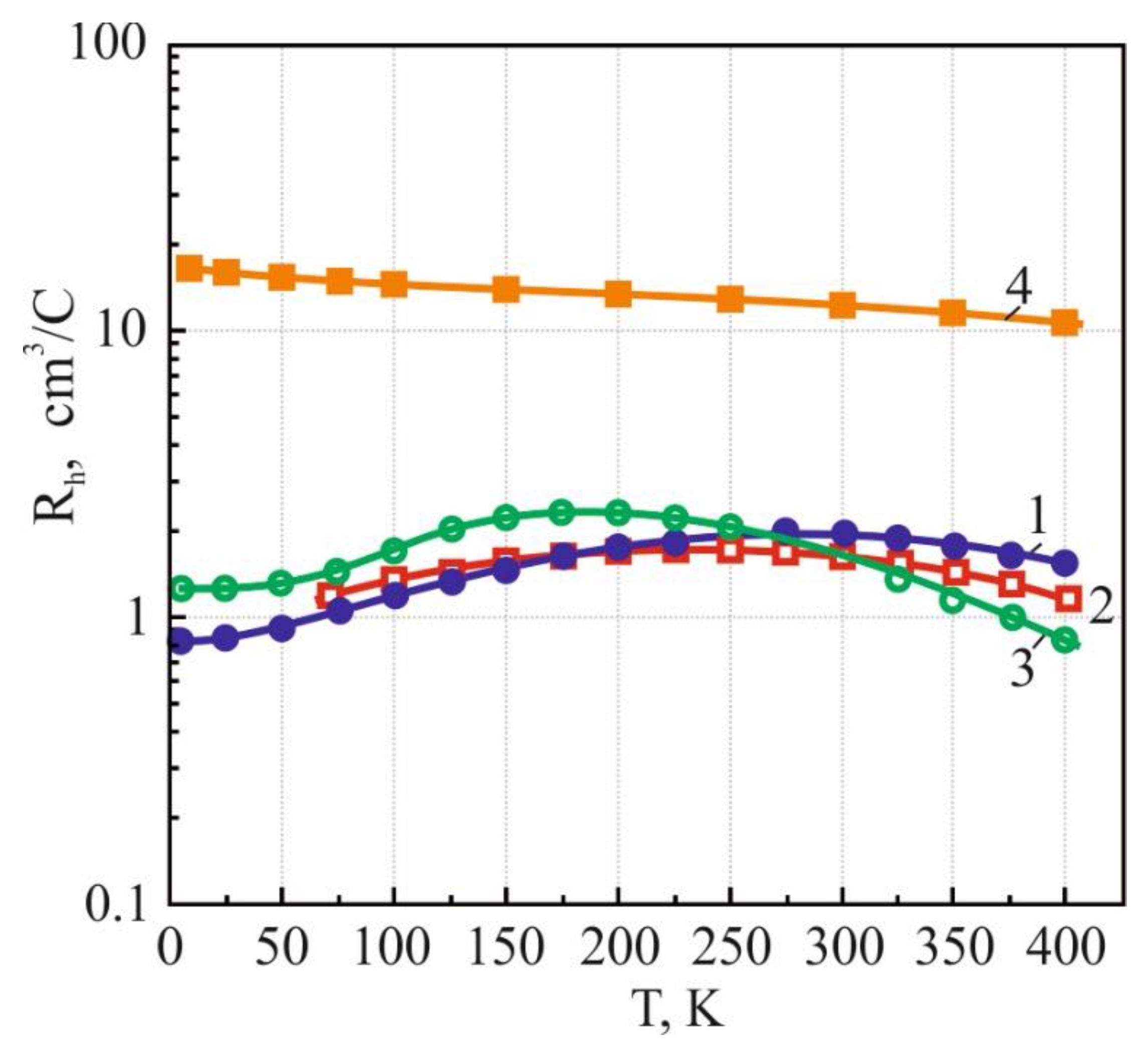
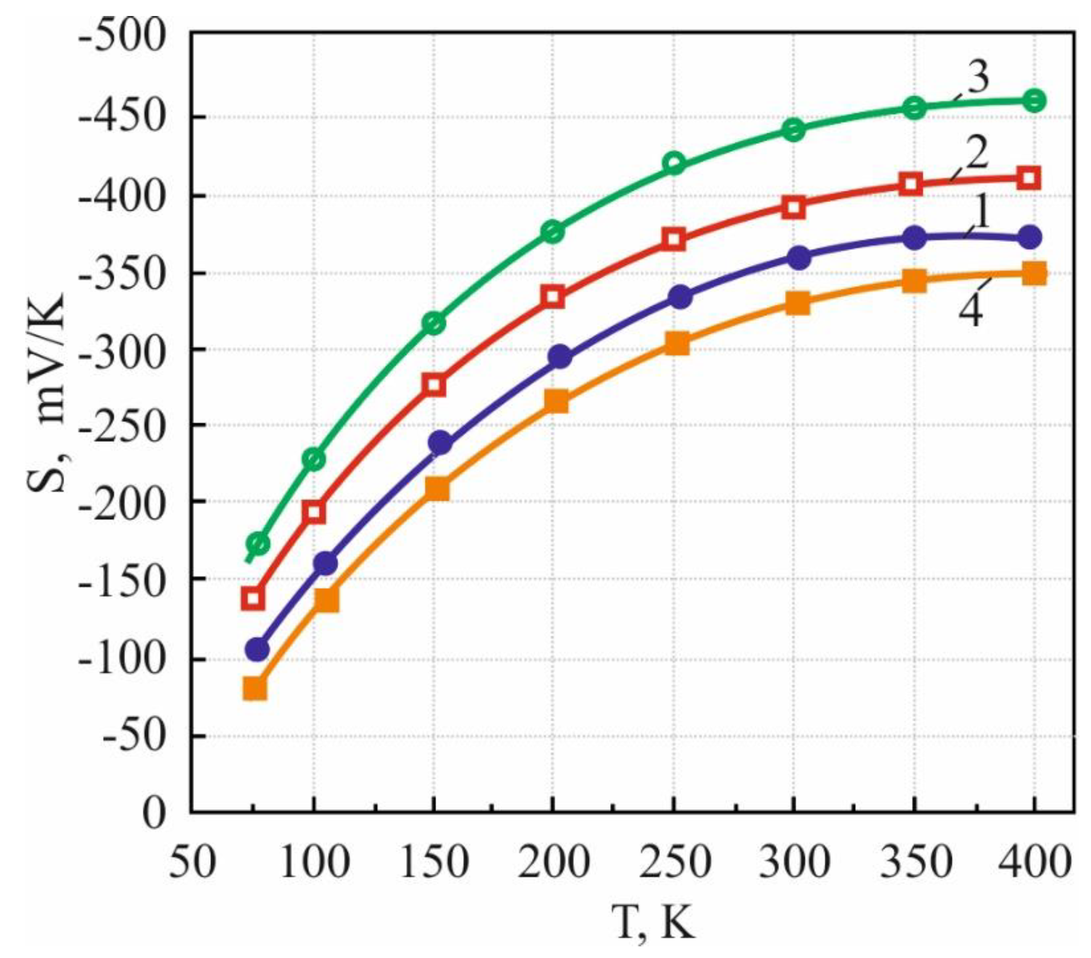
4. Thermoelectric Properties of Submicron Pb1−xInxTe Films on Polyimide Substrate

As presented in [34,36], a reliable method to control the electron concentration in the PbTe semiconductor is doping with indium—Pb1−xInxTe. Indium creates a resonance level in the conduction band over a wide temperature range [40,41].
Figure 11 demonstrates a temperature dependence of Hall coefficient RH from 10 to 400 K for Pb1−xInxTe films (x = 0.01, 0.002 and 0.03 at. %). All films have negative values of the Hall coefficient over the entire temperature range, which is related to the electronic conductivity (n- type) in PbTe films. The Hall concentration nH of the prepared Pb1−xInxTe films was determined using Equation (17). For all film specimens up to heavily doped Pb0.97In0.03Te film, the Hall electron concentration does not exceed in the order 1018 cm−3. A nonmonotonic temperature dependence of the Hall coefficient is observed, which is unusual for n- type PbTe films doped with donor iodine impurity [32].
The Fermi level EF was calculated from the electron concentration nH Equation (5) using a value of m n for bulk PbTe specimens ( m n ≈ 0.27 mo) [9]. EF is 0.06–0.08 eV above the bottom of the conduction band at a temperature of T ≤ 80 K. As the temperature increases, EF rapidly decreases, crossing the bottom of the conduction band at T = 250–350 K.
The Seebeck coefficient S for Pb1−xInxTe films also has negative values over the 80–400 K temperature range, typical to semiconductors with an electron type of conductivity (Figure 12). The value of S for Pb0.97In0.03Te achieves ≈−450 μV/K at T = 300 K. Figure 13 presents electrical conductivity σ as a function of temperature. The behavior of σ(T) is different from the temperature dependence of S(T). An increase in the content of the indium dopant in PbTe leads to a decrease in the electrical conductivity σ in the entire operation temperature range. Such unusual behavior of σ can be explained by a strong decrease in electron mobility μH with a growth of indium concentration in PbTe films.
Table 2 presents the thermoelectric properties at T = 300 K for polycrystalline n-PbTe1−xInxTe and PbTe0.999I0.001Te films on a thin polyimide substrate with a thickness of 1 ± 0.1 μm. The thermoelectric parameters of bulk n-type Pb1−xInxTe1−yTe specimens are also shown in Table 2. The calculated thermoelectric figure of merit Z for the n-Pb0.99In0.01Te film with the concentration n = 3 × 1018 cm−3 achieves the value Z ≈ 1.0 × 10⁻³ K−1 at 300 K, which is close to the Z value for n-PbTe bulk crystals doped with In [34] or codoped with In and I [42]. The lattice thermal conductivity κL was calculated according to Equations (8) and (10), and is also presented in Table 2. A significant decrease in the value of κL in polycrystalline Pb1-xInxTe films in comparison with bulk crystals [34,42] may be attributed to the scattering of long wave phonons by the grain boundaries [43].
The parameter r for Pb1−xInxTe films has a value of 1.5–2 in the 200–300 K temperature range. The additional scattering in polycrystalline Pb1−xInxTe films can be related to the creation of energy barriers for electrons on the grain boundaries. The schematic view of the energy band diagram for Pb1−xInxTe films is presented in Figure 14. Such barriers allow fast electrons with energy of E > EF to pass through and delay the slow electrons E < EF.

5. Application

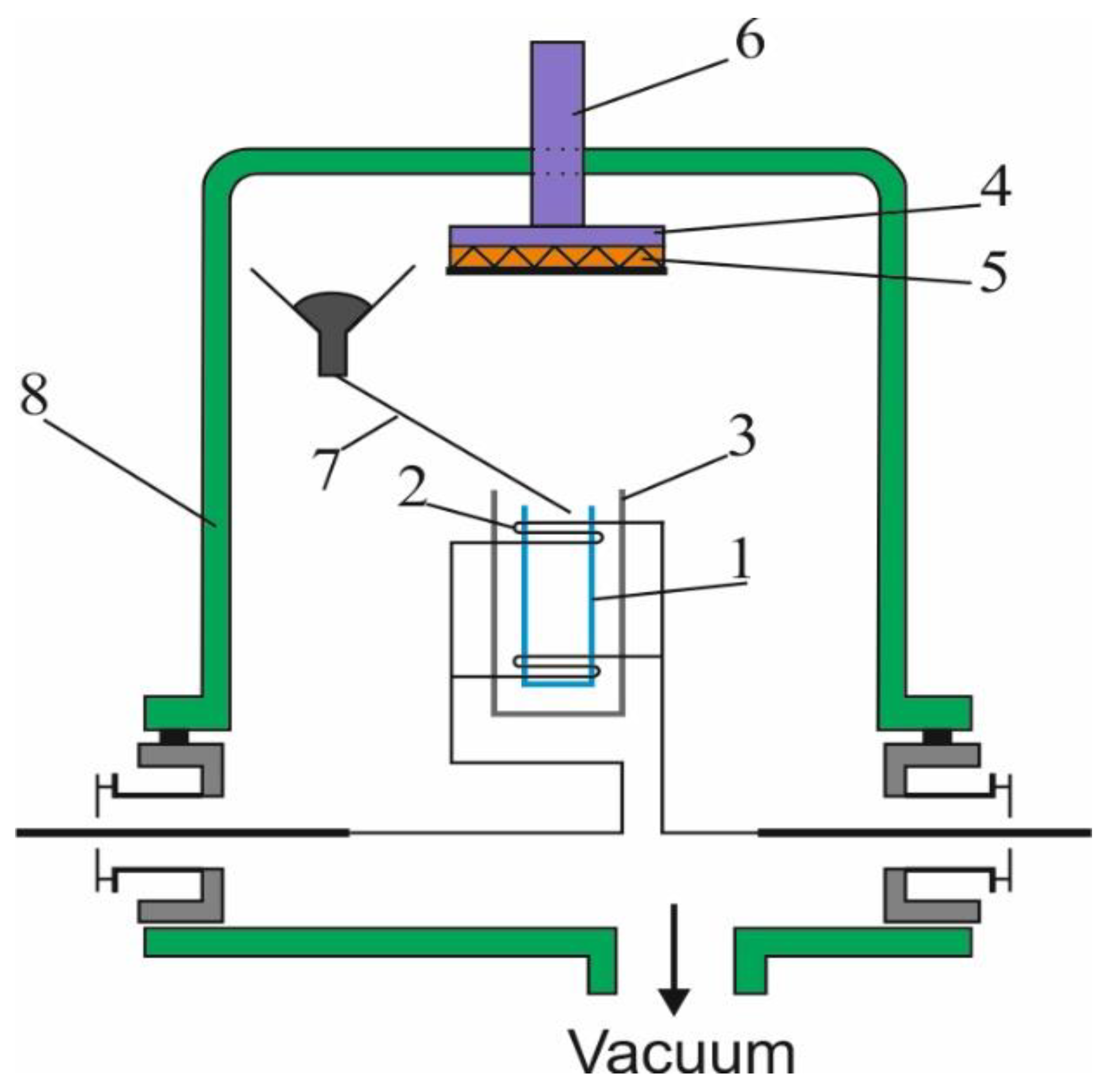
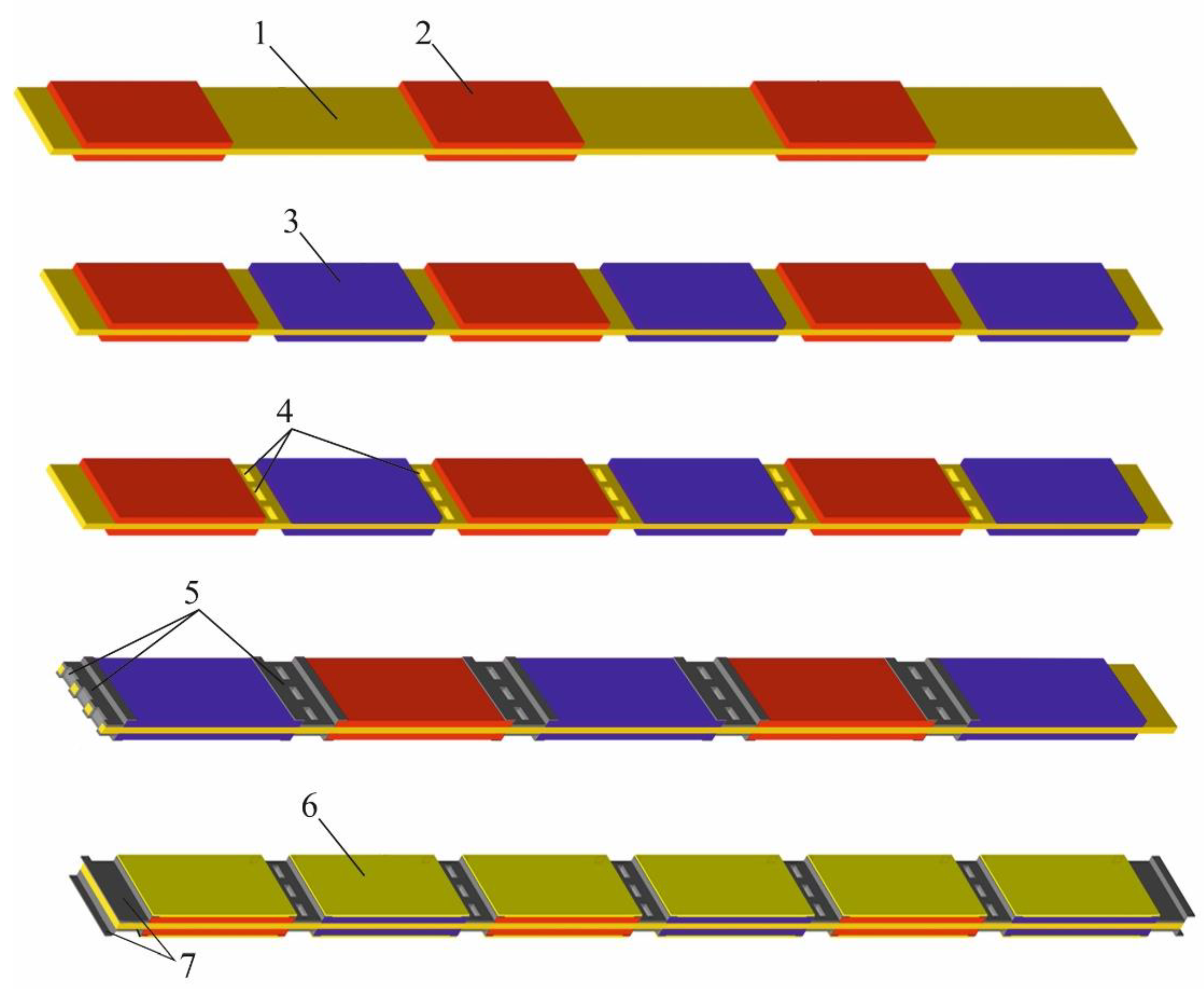
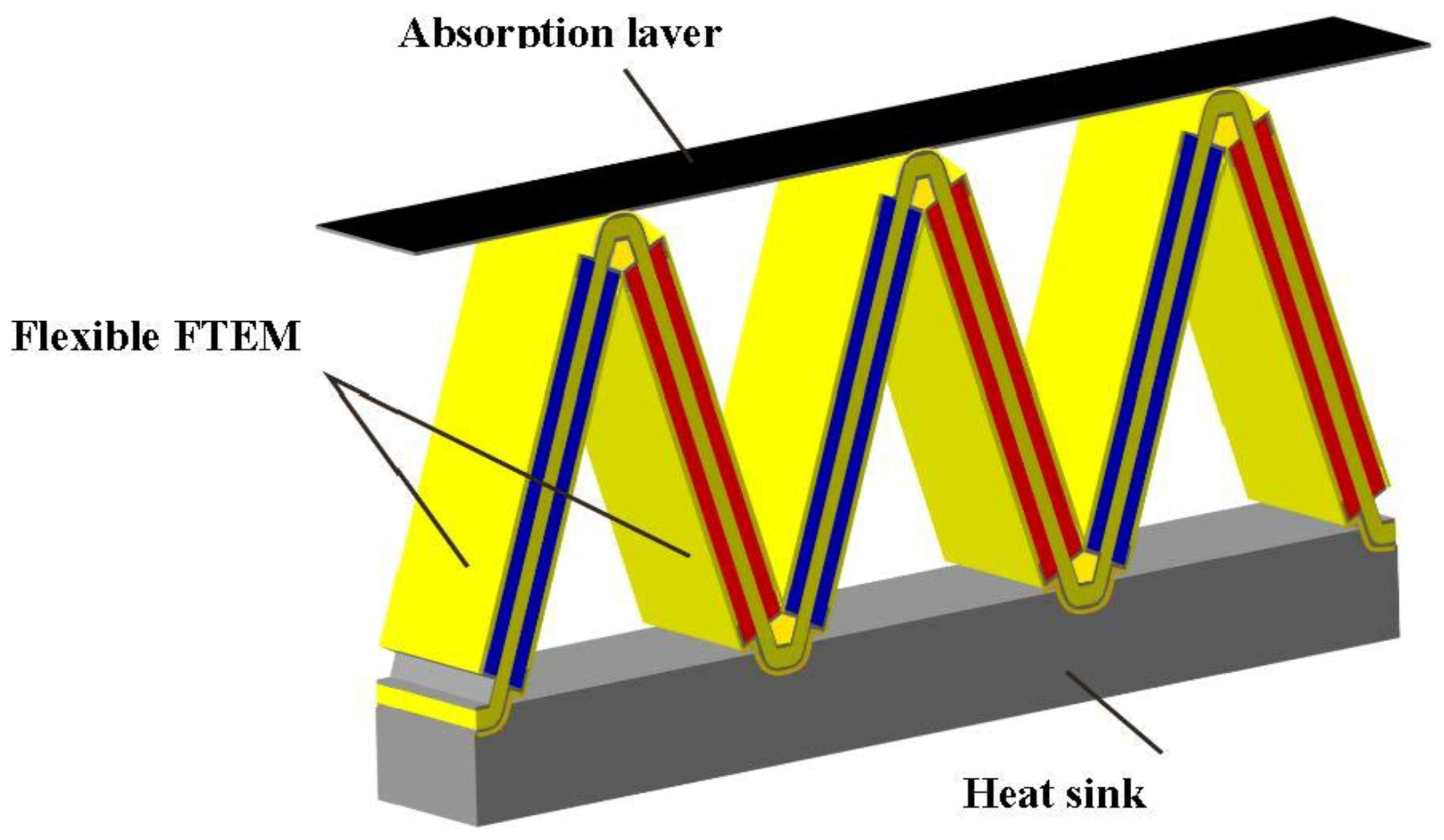
5.1. Film Thermoelectric Module

The challenge in thermoelectricity is the development of film thermoelectric batteries (modules) for miniature autonomic generators. Such devices were presented in [44,45,46,47,48].
The high performance a film thermoelectric module (FTEM) on a thin polyimide substrate using effective Bi2Te3 thermoelectrics was developed and presented in [49]. The fabrication of FTEM is described as follows (Figure 15):
  • Preparation of submicron p-type Bi0.5Sb1.5Te3 layers [11] (the thickness ~5 μm) on two sides of the flexible substrate (the thickness ~10 μm);
  • Preparation of submicron n-type Pb0.99In0.01Te layers (the thickness ~5 μm) on two sides of the flexible substrate;
  • Perforation between p- and n-type layers. The width of the cut ~0.2 mm, and a length between the cuts ~1 mm;
  • Preparation of the electrical contacts (two layers: the first Cr—with thickness ~0.1 μm and the second Au—with thickness ~0.5 μm) on the two sides of flexible substrate between the p- and n-type layers;
  • Preparation of a polymeric cover (the thickness ~0.5 mm) on two sides of the film thermoelectric module [50].
The characteristics of the FTEM (number of thermocouples N = 100) are presented in Table 3.

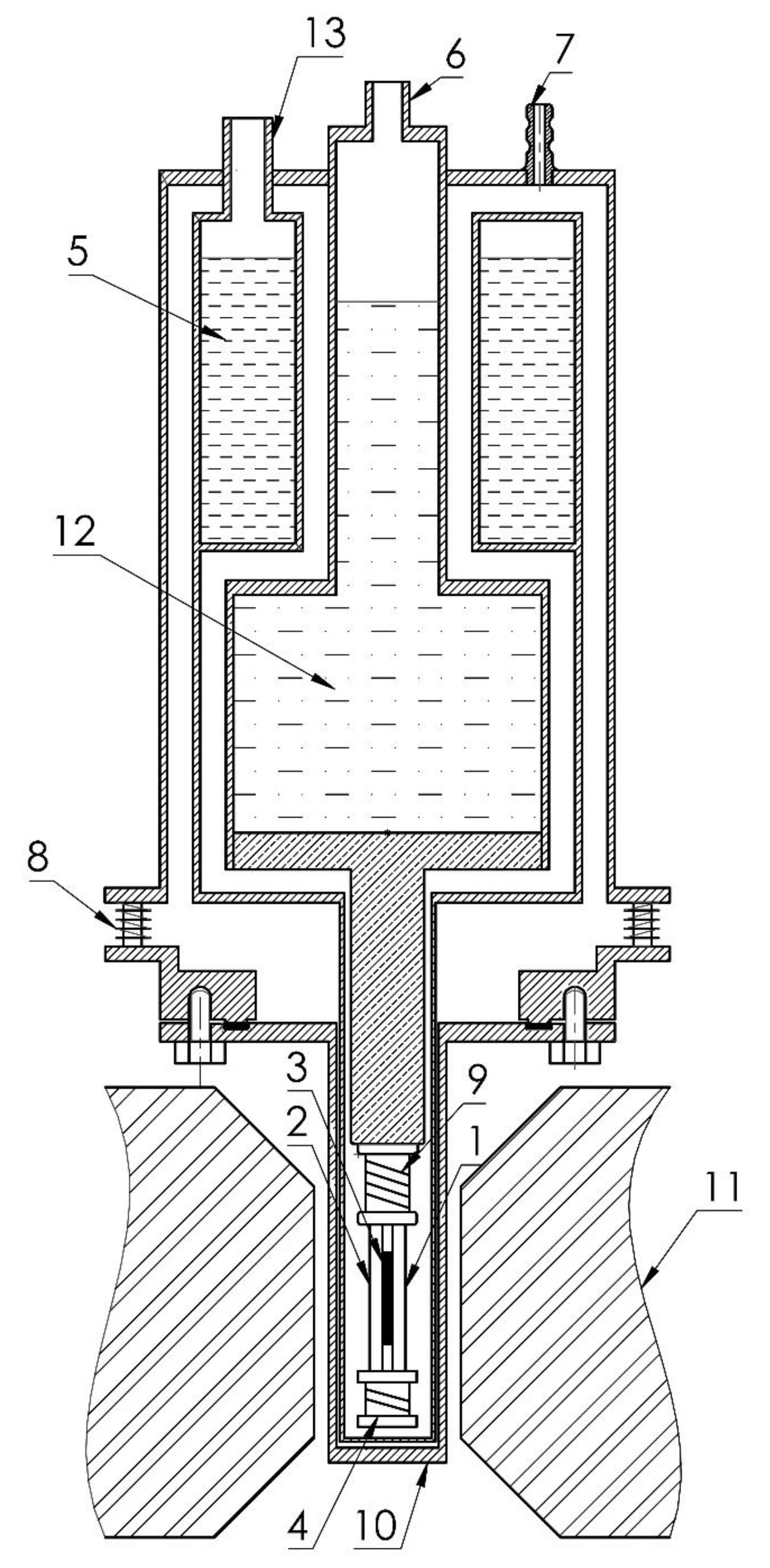
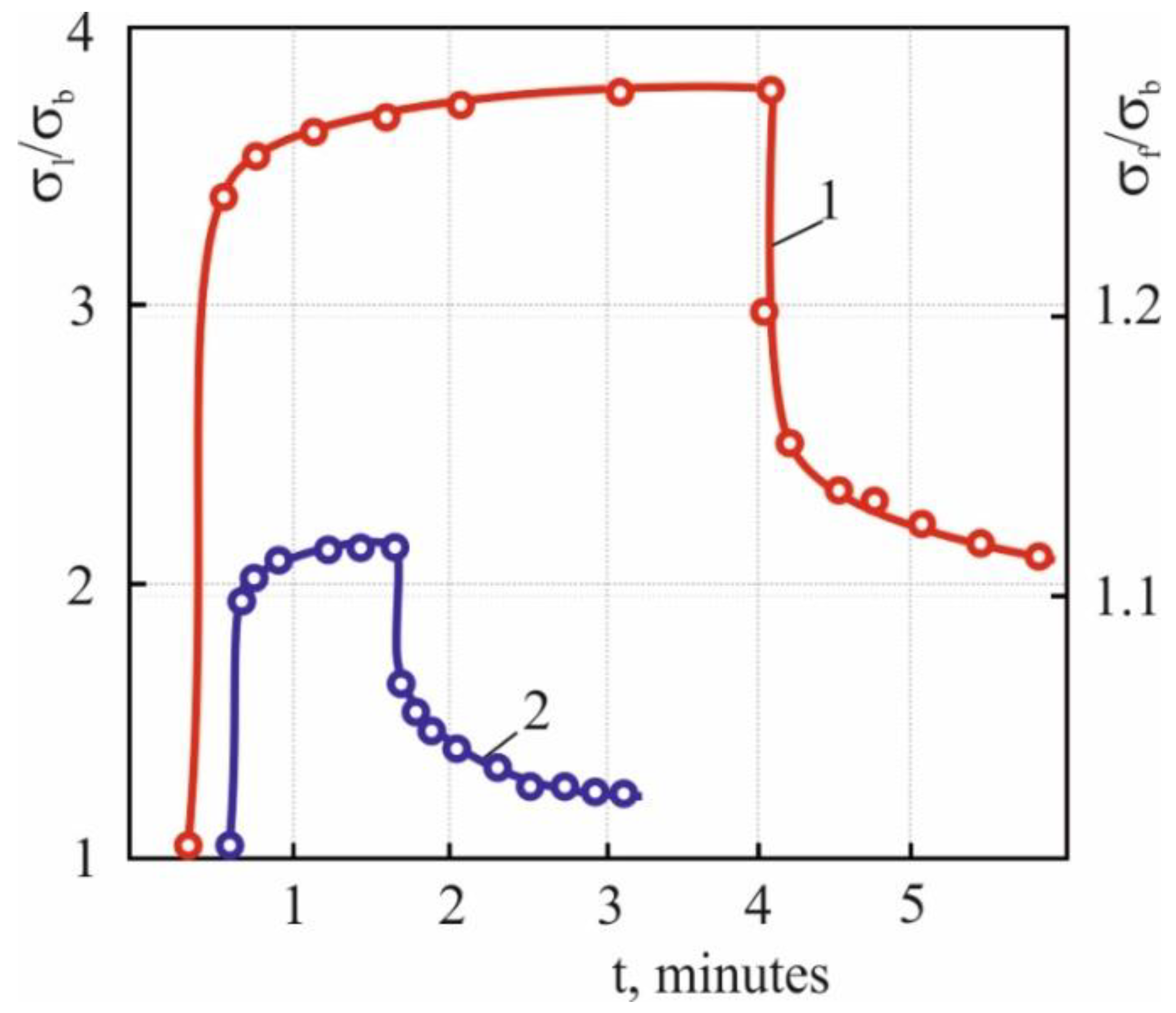
5.2. Film Thermoelectric Detector

Thermal detectors are heated by incident IR radiation. Their temperature increase may be measured by any temperature-dependent mechanism, such as thermoelectric voltage [51]. The design of a film thermoelectric detector (FTED) is presented in Figure 16. The flexible thin substrate with a thickness d ~10–12 μm and perforation cuts between the p- and n-film layers is bended along the perforations. The film thermoelectric detector (FTED) consists from an absorption layer, film thermoelectric module (FTEM), and a heat sink. The temperature difference between the hot and cold sides of FTEM creates an electrical voltage that is directly proportional to the power of the incoming radiation.
The main characteristics of a thermoelectric detector are the response time τr and sensitivity Ss [51]. The calculation of these parameters for a concrete design of FTED is given in [50]. In the case where the heat transfer is mainly determined by the process of heat conduction, the response time of such FTED (Figure 16) is determined by [50]:
τ r 4 π 2 c γ H 2 κ ,
where c is the heat capacity of the thermoelectric films, γ is their density, H is the height of thermocouples, and κ is the thermal conductivity of the thermoelectric films.
The response time as a function of the thickness of the thermoelectric film df and the height (length) of thermocouple H is presented in Table 4. The sensitivity Ss is defined by [51]:
S s = V / P ,
where V is the voltage, and P is the power of the incident radiation. V is determined for a thermoelectric detector by
V = ( S n + S p ) m ,
where Sn and Sp are Seebeck coefficients of the n- and p- film thermoelectric legs, and m is the number of thermocouples. The sensitivity Ss as a function of the thickness of thermoelectric film df and the height of thermocouple H for FTEB is listed in Table 4.

6. Conclusions

The transport properties of the Hall coefficient, Seebeck coefficient, electrical conductivity, and Nernst-Ettinshausen coefficient over the temperature range of 80–300 K were investigated for the nano(submicron) grained films of lead chalcogenide semiconductors (n- and p-type PbTe and n- and p-type PbSe) on an amorphous (polyimide) substrate.
The experimental measurements show a decrease in the electric conductivity and carrier mobility that is accompanied with an increase in the Seebeck coefficient of submicron-grained films of the lead chalcogenides. These properties result in an increase of the figure of merit Z for the submicron-grained Pb1−xInxTe films on the polyimide substrate. A model which may account for the beneficial properties of the films was presented and discussed in some detail. It assumes that a mountain ridge-like with alternating peaks potential relief is built along the grain boundaries. It scatters electrons with energy lower than the potential relief, which behaves as an energy barrier for them, and it does not affect electrons with higher energy. The model was assessed by magnetoresistance and photoconductivity experiments.
A Flexible Film Thermoelectric Module (FTEM) based on the p-type Bi2−xSbxTe3 and n-type, In-doped, PbTe materials on a thin polyimide substrate was developed. The dimensionless figure of merit ZT was ~0.4 and the TE efficiency ηmax ≈ 2.2% at temperature difference ΔT = 100 K (Tc = 300 K, Th = 400 K). The original design of a parallel-serial connection sharply increased the reliability of the FTEM, even if the number of thermoelectric unicouples was large (N ≥ 100). FTEM may be used as a radiation detector for short laser pulse diagnostics applications.

Author Contributions

Z.D.—principal investigator; S.M.—methodology; B.D.—investigation and visualization; M.A.—project management and conceptualization; R.Z.S.—supervision. All authors have read and agreed to the published version of the manuscript.

Funding

This research received no external funding.

Data Availability Statement

The raw/processed data required to reproduce these findings cannot be shared at this time, as the data also form part of an ongoing study.

Conflicts of Interest

The authors declare that they have no conflict of interest.

References

  1. Vineis, C.J.; Shakouri, A.; Majumdar, A.; Kanatzidis, M.G. Nanostructured thermoelectrics: Big efficiency gains from small features. Adv. Mater. 2010, 22, 3970–3980. [Google Scholar] [CrossRef] [PubMed]
  2. Chauhan, N.S.; Bathula, S.; Gahtori, B.; Yury, V.; Kolenko, Y.V.; Shyam, R.; Upadhyay, N.K.; Dhar, A. Spinodal decomposition in (Ti, Zr)CoSb half-Heusler: A nanostructuring route toward high efficiency thermoelectric materials. J. Appl. Phys. 2019, 126, 125110. [Google Scholar] [CrossRef]
  3. Sadek, A.; Salem, H.G. Controlling the Processing Parameters for Consolidation of Nanopowders into Bulk Nanostructured Material. In Processing of Nanoparticle Structures and Composites; Hinklin, T., Lu, K., Eds.; American Ceramic Society: Westerville, OH, USA, 2009; pp. 11–22. [Google Scholar]
  4. Liu, H.; Zhang, X.; Bu, Z.; Li, W.; Pei, Y. Thermoelectric properties of (GeTe)1−x[(Ag2Te)0.4(Sb2Te3)0.6]x alloys. Rare Met. 2022, 41, 921–930. [Google Scholar] [CrossRef]
  5. Tan, X.Y.; Dong, J.-F.; Jia, N.; Zhang, H.-X.; Ji, R.; Suwardi, A.; Li, Z.-L.; Zhu, Q.; Xu, J.-W.; Yan, Q.-Y. Enhanced near-room-temperature thermoelectric performance in GeTe. Rare Met. 2022, 41, 3027–3034. [Google Scholar] [CrossRef]
  6. Wang, H.; Liu, X.; Zhou, Z.; Wu, H.; Chen, Y.; Zhang, B.; Wang, G.; Zhou, X.; Han, G. Constructing n-type Ag2Se/CNTs composites toward synergistically enhanced thermoelectric and mechanical performance. Acta Mater. 2022, 223, 117502. [Google Scholar] [CrossRef]
  7. Cao, J.; Dong, J.; Saglik, K.; Zhang, D.; Solco, S.F.; You, I.J.; Liu, H.; Zhu, Q.; Xu, J.; Wu, J.; et al. Non-equilibrium strategy for enhancing thermoelectric properties and improving stability of AgSbTe2. Nano Energy 2023, 107, 108118. [Google Scholar] [CrossRef]
  8. Dashevsky, Z.; Skipidarov, S. Investigating the performance of bismuth-antimony telluride. In Novel Thermoelectric Materials and Device Design Concepts; Springer: Berlin/Heidelberg, Germany, 2019; pp. 3–21. [Google Scholar]
  9. Ravich, Y.I.; Efimova, B.A.; Smirnov, I.A. Semiconducting Lead Chalcogenides; Plenum Press: New York, NY, USA, 1970. [Google Scholar]
  10. Goltsman, B.M.; Dashevskii, Z.M.; Kaidanov, V.I.; Kolomoets, N.V. Film Thermoelements: Physics and Application; Nauka: Moscow, Russia, 1985. (In Russian) [Google Scholar]
  11. Parashchuk, T.; Kostyuk, O.; Nykyruy, L.; Dashevsky, Z. High thermoelectric performance of p-type Bi0.5Sb1.5Te3 films on flexible substrate. Mater. Chem. Phys. 2020, 253, 123427. [Google Scholar] [CrossRef]
  12. Dashevsky, Z. High photosensitive films of lead chalcogenides. In Handbook of Semiconductor Nanostructures and Nanodevices physics; Balandin, A., Wang, K., Eds.; American Scientific Publishes: Valencia, CA, USA, 2006; Volume 2, pp. 335–359. [Google Scholar]
  13. Dashevsky, Z.; Kreizman, R.; Dariel, M.P. Physical properties and inversion of conductivity type in nanocrystalline PbTe films. J. Appl. Phys. 2005, 98, 094309. [Google Scholar] [CrossRef]
  14. Komissarova, T.; Khokhlov, D.; Ryabova, L.; Dashevsky, Z.; Kasiyan, V. Impedance of photosensitive nanocrystalline PbTe (In) films. Phys. Rev. B 2007, 75, 195326–195330. [Google Scholar] [CrossRef]
  15. Dashevsky, Z.; Kasiyan, V.; Radovsky, G.; Shufer, E.; Auslender, M. Mid-Infrared Photoluminescence PbSe Film Structures up to Room Temperature; SPIE: Riga, Latvia, 2008; pp. 14–720. [Google Scholar]
  16. Dobrovolsky, A.; Komissarova, T.; Akimov, B.; Khokhlov, D.; Ryabova, L.; Dashevsky, Z. Charge transport in photosensitive nanocrystalline PbTe (In) films an alternating electric field. Int. J. Mater. Res. 2009, 100, 1252–1254. [Google Scholar] [CrossRef]
  17. Dobrovolsky, A.; Ryabova, L.; Khokhlov, D.; Dashevsky, Z.; Kasiyan, V. Low temperature charge transport in photosensitive nanocrystalline PbTe (In) films. J. Phys. Conf. Ser. 2009, 150, 220–225. [Google Scholar] [CrossRef]
  18. Dashevsky, Z.; Kreizman, R.; Shufer, E.; Kasiyan, V.; Flitsiyan, E.; Shatkhin, M.; Chernyak, L. Nanocrystalline PbTe films. J. Nanoelectron. Optoelectron. 2009, 4, 296–301. [Google Scholar] [CrossRef]
  19. Radovsky, G.; Dashevsky, Z.; Kasiyan, V.; Auslender, M.; Hava, S. Polycrystalline PbSe on a Polyimide substrate. J. Alloy. Compd. 2010, 501, 6–13. [Google Scholar] [CrossRef]
  20. Dobrovolsky, A.; Chernichkin, V.; Belogorokhov, I.; Dashevsky, Z.; Kasiyan, V.; Ryabova, L.; Khokhlov, D. Transport properties and photo- conductivity of nanocrystalline PbTe (In) films. Phys. Status Solidi C 2010, 7, 869–872. [Google Scholar] [CrossRef]
  21. Chernichkin, V.; Dobrovolsky, A.A.; Ryabova, L.; Khokhlov, D.; Dashevsky, Z. Photoconductivity of PbTe: In films with variable microstructure. Semiconductors 2011, 45, 1474–1478. [Google Scholar] [CrossRef]
  22. Chernichkin, V.; Dobrovolsky, A.A.; Ryabova, L.; Khokhlov, D.; Dashevsky, Z. Observation of local electron states linked to the quasi-Fermi level. EPL 2012, 100, 17008. [Google Scholar] [CrossRef]
  23. Kovalyuk, V.; Sheveleva, E.; Auslender, M.; Goltsman, G.; Shneck, R.; Dashevsky, Z. Polycrystalline PbTe: In films on amorphous substrate. Structure and physical properties. Materials 2022, 15, 8383. [Google Scholar] [CrossRef]
  24. Dobrovolsky, A.; Ryabova, L.; Khokhlov, D.; Dashevsky, Z.; Kasiyan, V. Photoconductivity of oxidized nanostrucrued PbTe (In) films. Semicond. Sci. Technol. 2009, 24, 750–755. [Google Scholar] [CrossRef]
  25. Kreizman, R.; Traistman, N.; Shaked, M.; Dashevsky, Z.; Dariel, M.P. Thin films of PbTe semiconductors, the influence of oxygen on the electric properties bulk and thin films of PbTe semiconductors. Key Eng. Mater. 2007, 336, 875–878. [Google Scholar] [CrossRef]
  26. Park, S.J.; Cho, K.S.; Kim, S.H. A study of dielectric characteristics of polyimide thin film. J. Colloid Interface Sci. 2004, 272, 384. [Google Scholar] [CrossRef]
  27. Bode, D.E.; Levinstein, H. Effect of oxygen on the electrical properties of lead telluride films. Phys. Rev. 1954, 96, 259. [Google Scholar] [CrossRef]
  28. Dobrovolsky, A.; Komissarova, T.; Dashevsky, Z.; Kassiyan, V.; Akimov, B.; Ryabova, L.; Khokhlov, D. Effect of oxidation on the conductivity of nanocrystalline PbTe: In films in an alternating electric field. Semiconductors 2009, 43, 253–256. [Google Scholar] [CrossRef]
  29. Dashevsky, Z.; Shufer, E.; Kasiyan, V.; Flitsiyan, E.; Chernyak, L. Influence of oxygen treatment on transport properties of PbTe: In polycrystalline films. Phys. B Condens. Matter 2010, 405, 2380–2384. [Google Scholar] [CrossRef]
  30. Shufer, E.; Dashevsky, Z.; Kasiyan, V.; Flitsiyan, E.; Chernyak, L.; Gartsman, K. Electrical conductivity and minority carrier diffusion in thermally oxidized PbTe thin films. Phys. B Condens. Matter 2010, 405, 1058–1061. [Google Scholar] [CrossRef]
  31. Jost, S. Identifying the physical mechanisms of polycrystalline lead salt photoconductors. J. Appl. Phys. 2022, 132, 064503. [Google Scholar] [CrossRef]
  32. Dzundza, B.; Nykyruy, L.; Parashchuk, T.; Ivakin, E.; Yavorsky, Y.; Chernyak, L.; Dashevsky, Z. Transport and thermoelectric performance of n-type PbTe films. J. Phys. B 2020, 588, 412178. [Google Scholar] [CrossRef]
  33. Ivakin, E.V.; Tolstik, A.L.; Gorbach, D.V.; Stankevich, A. Investigation of heat transfer of bulk and thin film PbInTe samples by the metod of dynamic grating. J. Eng. Phys. Thermophys. 2022, 95, 1026–1030. [Google Scholar] [CrossRef]
  34. Parashchuk, T.; Dashevsky, Z.; Wojciechowski, K. Feasibility of a high stable PbTe: In semiconductor for thermoelectric energy applications. J. Appl. Phys. 2019, 125, 245103. [Google Scholar] [CrossRef]
  35. Dariel, M.P.; Dashevsky, Z.; Jarashnely, A.; Shusterman, S.; Horowitz, A. Carrier concentration gradient generated in p-type PbTe crystals by unidirection solidification. J. Cryst. Growth 2002, 234, 164–170. [Google Scholar] [CrossRef]
  36. Dashevsky, Z.; Shusterman, S.; Dariel, M.P.; Drabkin, I. Thermoelectric efficiency in graded indium-doped crystals. J. Appl. Phys. 2002, 92, 1425–1430. [Google Scholar] [CrossRef]
  37. Gradauskas, J.; Dzundza, B.; Chernyak, L.; Dashevsky, Z. Two-color infrared sensors on the PbTe: In p-n junction. Sensors 2021, 21, 1195. [Google Scholar] [CrossRef] [PubMed]
  38. Young, D.L.; Coutts, T.J.; Kaydanov, V.I. Density-of-states effective mass and scattering parameter measurements by transport phenomena in thin films. Rev. Sci. Instrum. 2000, 71, 462–466. [Google Scholar] [CrossRef]
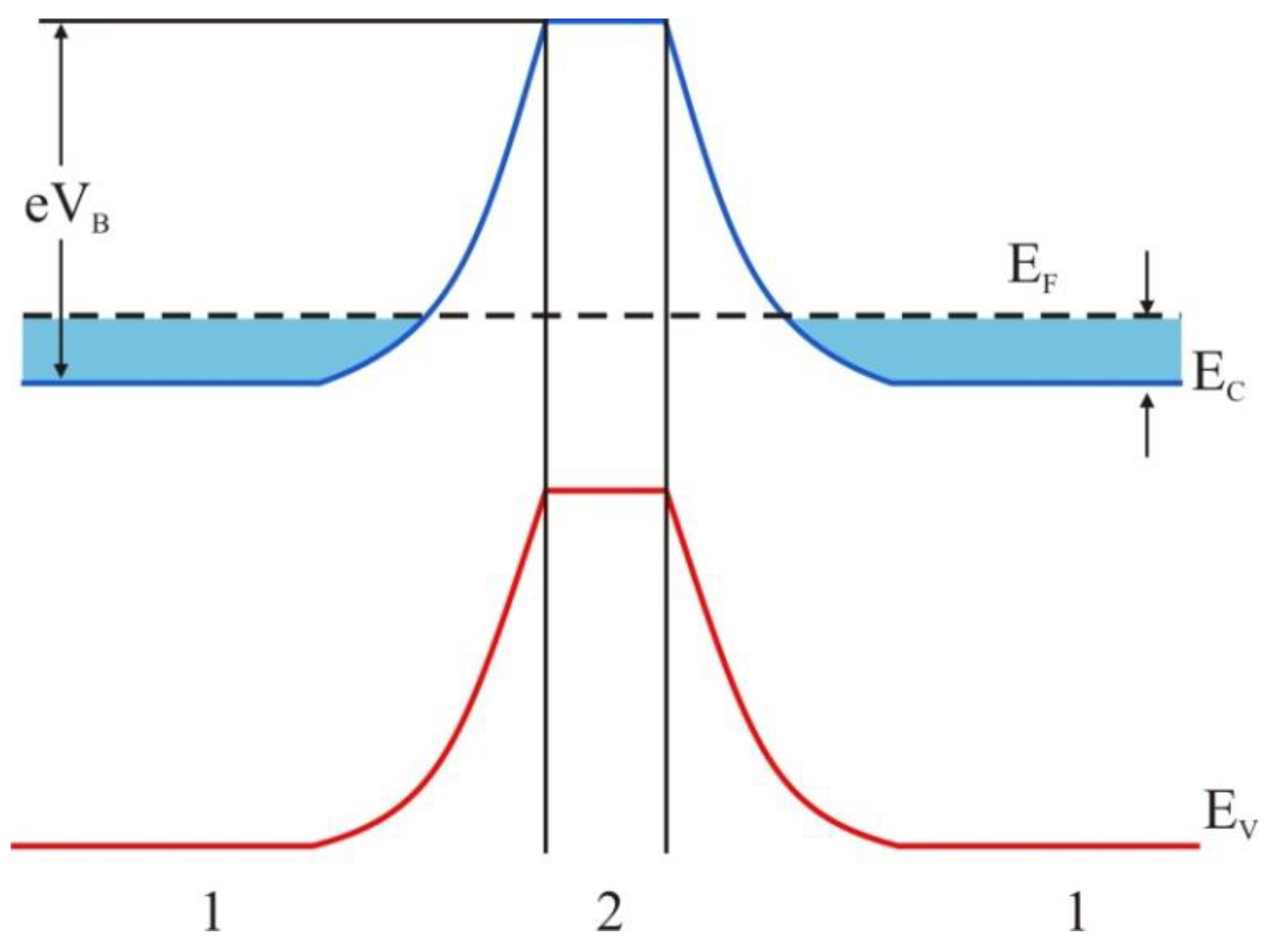
  39. Neophytou, N.; Kosina, H. Optimizing thermoelectric power factor by means of a potential barrier. J. Appl. Phys. 2013, 114, 044315. [Google Scholar] [CrossRef]
  40. Kaidanov, V.I.; Ravich, Y.I. Deep and resonance states in AIV BVI semiconductors. Sov. Phys. Usp. 1985, 28, 31–53. [Google Scholar] [CrossRef]
  41. Volkov, B.A.; Ryabova, L.I.; Khokhlov, D.P. Mixed-valence impurities in lead telluride-based solid solutions. Phys. Usp. 2002, 45, 819. [Google Scholar] [CrossRef]
  42. Wojciechowski, K.; Parashchuk, T.; Wiendlocha, B.; Cherniushok, O.; Dashevsky, Z. Highly efficient n-type PbTe developed by advanced electronic structure engineering. J. Mater. Chem. C 2020, 38, 13270. [Google Scholar] [CrossRef]
  43. Kuo, J.J.; Wood, M.; Slade, T.J.; Kanatzidis, M.G.; Snyder, G.J. Systematic over-estimation of lattice thermal conductivity in materials with electrically-resistive grain boundaries. Energy Environ. Sci. 2020, 13, 1250–1258. [Google Scholar] [CrossRef]
  44. Karthikeyan, V.; Surjadi, J.U.; Wong, J.C.; Kannan, V.; Lam, K.H.; Chen, X.; Lu, Y.; Roy, V.A. Wearable and flexible thin film thermoelectric module for multi-scale energy harvesting. J. Power Sources 2020, 455, 227983. [Google Scholar] [CrossRef]
  45. Tappura, K.; Jaakkola, K. A Thin-film thermoelectric generator forl large-Area Applications. Proceedings 2018, 2, 779. [Google Scholar]
  46. Settaluri, K.T.; Lo, H.; Ram, R.J. Thin Thermoelectric Generator System for Body Energy Harvesting. J. Electron. Mater. 2012, 41, 984. [Google Scholar] [CrossRef]
  47. Venkatasubramanian, R.; Siivola, E.; Colpitts, T.; O’Quinn, B. Thin-film thermoelectric devices with high room-temperature figures of merit. Nature 2001, 413, 597. [Google Scholar] [CrossRef] [PubMed]
  48. Fan, P.; Zheng, Z.; Cai, Z.; Chen, T.; Liu, P.; Cai, X.; Zhang, D.; Liang, G.; Luo, J. The high performance of a thin film thermoelectric generator with heat flow running parallel to film surface. Appl. Phys. Let. 2013, 102, 033904. [Google Scholar] [CrossRef]
  49. Maksymuk, M.; Parashchuk, T.; Dzundza, B.; Nykyruy, L.; Chernyak, L.; Dashevsky, Z. Highly efficient bismuth telluride—based thermoelectric microconvertor. J. Mater. Today Energy 2021, 21, 100753. [Google Scholar] [CrossRef]
  50. Kostyuk, O.; Yavorsky, Y.; Dzundza, B.; Dashevsky, Z. Development of thermal detector based on flexible film thermoelectric module. J. Phys. Chem. Solid State 2022, 22, 45–52. [Google Scholar] [CrossRef]
  51. Rogalski, A. Infrared Detectors; CRC Press: Boca Raton, FL, USA, 2010. [Google Scholar]
Figure 1. The schematic view of the flash evaporation method [11]. (1): quartz crucible, (2): crucible heater, (3): heat shield, (4): substrate, (5): substrate heater, (6): liquid nitrogen tube, (7): powder vessel, (8): vacuum chamber.
Energies 16 03774 g001
Figure 2. Schematic view of set up for transport properties measurements over 10–300 K temperature range [32]. (1), (2): copper plates, (3): sample, (4): gradient heater, (5): reservoir for liquid nitrogen, (6): nozzle for liquid nitrogen filling, (7): nozzle for pumping out, (8): vacuum connector, (9): heater, (10): removable cover, (11): electromagnet core, (12): reservoir for liquid helium, (13): nozzle for liquid helium filling.
Energies 16 03774 g002
Figure 3. Scheme of implementing the method of dynamic gratings.
Energies 16 03774 g003
Figure 4. Scanning electron microscopy image for PbTe films on polyimide substrate. (a) Ts = 100 K. (b) Ts = 300 K. (c) Ts = 400 K. (d) Ts = 500 K. (e) Image of cross-section of PbTe film at Ts = 500 K.
Energies 16 03774 g004
Figure 5. XRD patterns of PbTe films on polyimide substrate for different Ts. 1–100 K, 2–300 K, 3–500 K.
Energies 16 03774 g005
Figure 6. Relative change of the Seebeck coefficient (1 and 2) and of electrical conductivity (3 and 4) as a function of electron concentration for n−type PbTe films on a polyimide substrate. Temperature T = 100 K for 1 and 4. T = 300 K for 2 and 3.
Energies 16 03774 g006
Figure 7. Relative change of the Seebeck coefficient S as a function of charge carrier concentrations n(p) for p−type (1, 2) and n−type (3, 4) PbSe films on a polyimide substrate. Temperature T = 120 K for 1 and 3. T = 300 K for 2 and 4.
Energies 16 03774 g007
Figure 8. Magnetoresistance as a function of carrier concentration in n−type PbSe films. (a) temperature T = 300 K. (b) temperature T = 80 K. Magnetic field B || (111) for specimens 1 and 3. В (111) for specimens 2 and 4.
Energies 16 03774 g008
Figure 9. The photoconductivity kinetics in p−type PbTe films. 1—p = 1 × 1018 cm−3 at temperature T = 80 K (left scale). 2—p = 5 × 1018 cm−3 at T = 80 K (right scale).
Energies 16 03774 g009
Figure 10. Schematic energy band diagram in Pb1−xInxTe film, consisting of grains and interlayers between grains. EF is the Fermi level, Edr is the drift barrier, and Erec is the recombination barrier.
Energies 16 03774 g010
Figure 11. Hall coefficient as a function of temperature for n−PbTe:In films (1–3) and PbTe:I film (4). 1—Pb0.99In0.01Te, 2—Pb0.98In0.02Te, 3—Pb0.97In0.03Te, 4—PbTe0.999I0.001 from [32].
Energies 16 03774 g011
Figure 12. Seebeck coefficient as a function of temperature for n−PbTe:In (1–3) and n−PbTe:I (4) films. (1): Pb0.99In0.01Te, (2): Pb0.98In0.02Te, (3): Pb0.97In0.03Te, and (4): PbTe0.999I0.001 from [32].
Energies 16 03774 g012
Figure 13. Electrical conductivity as a function of temperature for n−PbTe:In (1–3) and n−PbTe:I (4) films. (1): Pb0.99In0.01Te, (2): Pb0.98In0.02Te, (3): Pb0.97In0.03Te, and (4) PbTe0.999I0.001Te [32].
Energies 16 03774 g013
Figure 14. Schematic energy band diagram in Pb1−xInxTe film, consisting of (1): grains, and (2): boundaries between grains. EC is the edge of conduction band, EV is the edge of valence band, EF is the Fermi level, and eVB is the height of the energy barrier.
Energies 16 03774 g014
Figure 15. Schematic view of FTEM on thin flexible (polyimide) substrate. (1): substrate, (2): p−legs, (3): n−legs, (4): perforation, (5): commutation metallic layers, (6): isolated layer, and (7): output contacts.
Energies 16 03774 g015
Figure 16. Schematic design of a Film Thermoelectric Detector (FTED).
Energies 16 03774 g016
Table 1. The values of electron mobility μ and scattering parameter r in PbTe films and single crystals at different carrier concentration n.
Carrier Concentration n × 10−18, сm−3Fermi Level
μ*, eВ
μ1, cm2/Vsr1refμ2, cm2/Vsr2
60.07585000.81.669002.2
200.1349000.61.530002
1000.313000.551.511002.3
Table 2. Thermoelectric properties of n- type Pb1−xInxTe (1–3), PbTe1−yIy films, and Pb1−xInxTe1−yIy bulk specimens at the temperature T = 300 K.
CompositionS, μV/Kσ,
Ω−1cm−1
κ,
W/mK
κL,
W/m K
Z × 103,
K−1
Reference
Pb0.99In0.01Te−3501101.51.40.9-
Pb10.98In0.02Te−400701.41.40.8-
Pb0.97In0.03Te−440501.31.30.75-
PbTe0.999I0.0001−3301001.81.70.6[32]
Pb0.999In0.001Te−2056002.21.91.1[34]
Pb0.999In0.001Te0.999I0.001−15511002.52.01.05[42]
Table 3. Output parameters of the FTEM (Th = 400 K, Tc = 300 K) with the number of thermocouples N = 100, film thickness df = 10 µm, length l = 1 mm, and width b = 4 mm.
Dimensionless Figure of Merit
(ZT)av
Efficiency
η, %
Resistance
R, Ω
Electric Current IL, mAOutput Voltage
VL, V
Electric Power
PL, mW
0.372.27029258
Table 4. Response time τr and sensitivity Ss as a function of the thickness of thermoelectric film df and the height of thermocouple H for a Film Thermoelectric Detector (FTED).
H, mmResponse Time τr, sSensitivity Ss, V/W
df = 1 μmdf = 5 μmdf = 10 μmdf = 1 μmdf = 5 μmdf = 10 μm
11.50.90.7853515
25.12.52.01105835
3126.55.012010090
Disclaimer/Publisher’s Note: The statements, opinions and data contained in all publications are solely those of the individual author(s) and contributor(s) and not of MDPI and/or the editor(s). MDPI and/or the editor(s) disclaim responsibility for any injury to people or property resulting from any ideas, methods, instructions or products referred to in the content.

