Review

A Review of Different Types of Solar Cell Materials Employed in Bifacial Solar Photovoltaic Panel

by
Muthu Vimala
1,
Geetha Ramadas
1,
Muthaiya Perarasi
2,
Athikesavan Muthu Manokar
3 and
Ravishankar Sathyamurthy
4,5,*
1
Department of Electrical & Electronics Engineering, R.M.K. Engineering College, Chennai 601206, India
2
Department of Electronics and Communication Engineering, R.M.K. Engineering College, Chennai 601206, India
3
Department of Mechanical Engineering, B.S. Abdur Rahman Crescent Institute of Science and Technology, Chennai 600048, India
4
Department of Mechanical Engineering, King Fahd University of Petroleum and Minerals, Dhahran 31261, Saudi Arabia
5
Interdisciplinary Research Center for Renewable Energy and Power Systems (IRC-REPS), King Fahd University of Petroleum and Minerals, Dhahran 31261, Saudi Arabia
*
Author to whom correspondence should be addressed.
Energies 2023, 16(8), 3605; https://doi.org/10.3390/en16083605
Submission received: 21 February 2023 / Revised: 4 April 2023 / Accepted: 14 April 2023 / Published: 21 April 2023
(This article belongs to the Special Issue Review Papers in Energy and Buildings)

Abstract

:
Conventionally accessible silicon solar cells experience two major drawbacks, such as reduced efficiency and increased fabrication costs. The prospects for the reduction in the cost of the photovoltaic form of energy conversion are bifacial solar cells. Bifacial solar cells show potential opportunity in reducing the cost of solar energy conversion when analyzed with respect to monofacial cells. The bifacial solar cells exploit sunlight occurrence on both sides of the cell more efficiently. Bifacial-based solar photovoltaic (PV) is a technology that increases the generation of electrical energy per square meter of PV module through the utilization of light absorption from the albedo. This technology can generally be categorized based on the type of solar cell material and the fabrication technique. PV devices are classified as a silicon-based, thin film, organic, and advanced nano PV. This paper takes a second look at some recent initiatives and significant issues in enhancing the efficiency of bifacial solar cells from material sciences and chemical composition aspects. From this review, it is concluded that screen-printed solar cells have produced a maximum efficiency of 22%. Additionally, triode structure single-crystalline cells produced a maximum front side efficiency of 21.3% and rear side efficiency of 19.8%. Considering the recycling of solar panels, organic solar panels can be developed.

1. Introduction

The consumption of electricity has been gradually increasing all over the world on a daily basis. As a result, the demand for electricity is increasing exponentially. In 1931, Thomas Alva Edison mentioned the usage of solar power before fossil fuels become extinct from Earth. Presently, we are dependent on conventional sources, such as coal, oil, and gas, which are the principal sources of energy originating from carbon-based fossil fuels. However, the limiting factors in the availability and rising prices of all these sources are a major cause of concern for energy availability in the future. Environmental pollution also tends to rise, owing to the usage of the above-mentioned fossil fuels. These issues can be addressed to a great extent by moving towards renewable energy sources such as solar energy, which is available in India for almost 300 bright days a year. Additionally, solar energy is the cleanest source of energy, leading to a green and healthy environment. A system incorporated with solar energy can operate for almost 25 years without any considerable running cost; it is also the cheapest source of energy conversion in the long run. The advantages of the usage of solar cells are reduced electricity bills, reduced maintenance, low emissions, and feed-in tariffs and rebates. Under the Honorable Prime Minister’s “Make in India” program, the Suryamitra Skill Development Program is a flagship program with a goal to achieve 100 GW of solar power capacity by 2022 [1].
Bifacial Solar Cells (BSC) concurrently gather photons from the incident solar intensity and albedo radiation, receiving both the front side and back side of a device, whereas monofacial solar cells are able to collect only those photons from the incident solar intensity on the front side of the solar module. Since the 1960s, these BSC have been researched [2] and were first characterized in the scientific literature by Luque et al. [3] as a novel thought for increasing the energy yield output of PV systems. An enhancement of 50% in electric power production can be achieved at once by collecting both the direct and albedo radiation from the rooftop and the environment around a module with the help of a focused device, as presented by Cuevas et al. [4]. Accordingly, it was demonstrated that even BSC amplifies the power density of PV modules compared with monofacial cells and, at the same time, reduces the cost of the PV system [5]. An additional benefit of BSC is the reduction in the working temperature of the cell and the equivalent augmentation in the highest power production, which is due to the condensed infrared absorption in aluminum back metallization absence, even though there is an add-on in thermal insulation on the rear side of the bifacial module rather than the conventional rear sheet cover [6,7,8]. The cross-sectional view of the majority of frequently fashioned bifacial crystalline silicon (Si) solar cells is shown in Figure 1. In a sequence to collect illumination from either side or both concurrently, an open metallization grid is written. For the cells of n-type, the p+ diffused layer will act as the emitter, while the n+ layer serves as a Back-Surface Field (BSF), and vice versa, for the p-type solar cells. In order to realize the open metallization grid at trade-making scales, passivizing anti-reflective coatings (ARC) and texturized wafers are moderately covered by screen-printed metallic contacts [9].

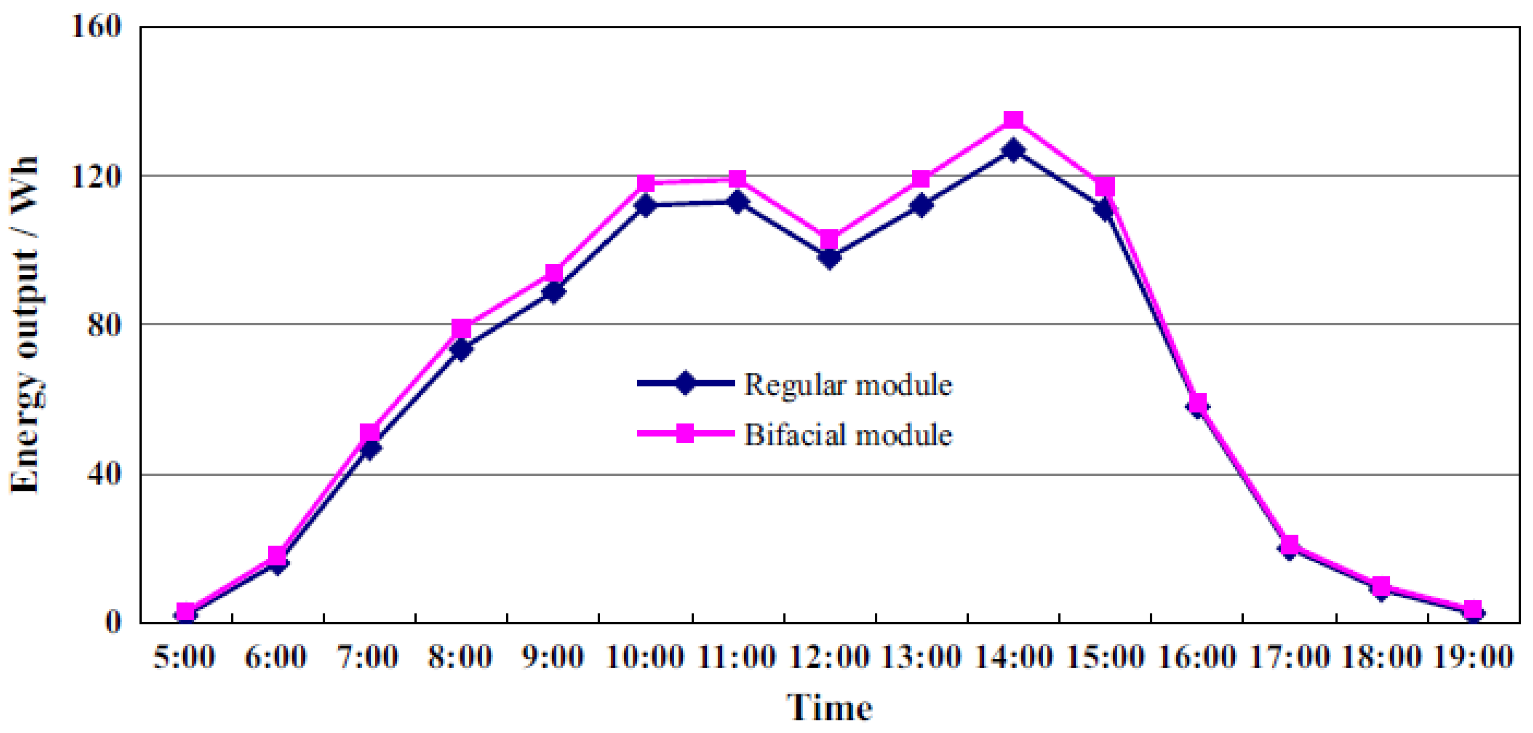
2. Different Types of Solar Cell Materials Employed in Bifacial Solar PV Panel

Andreas Hubner [10] experimented with the temperature performance of monofacial and bifacial Si solar cells by calculating the absorption of Infrared Radiation (IR) in both cells. The representation diagram of the projected Si solar cell with a thickness of 300 μm and 1.5 Ω cm float-zone (FZ) Si wafers is shown in Figure 2. It is proved experimentally that above 1200 nm, monofacial cells absorb IR about 68%, whereas bifacial cells absorbed only 36% of IR. Additionally, a 6.5% of energy absorption difference is recorded in terms of the AM1.5G spectrum between the monofacial and bifacial cells.
Andreas Hubner et al. [11] also fabricated a new cost-effective PV energy bifacial cell by combining Plasma-Enhanced Chemical Vapor Deposition (PECVD) Si nitride film, which has excellent surface passivation properties with simple alloyed Aluminum (Al) BSF. The importance of Al BSF was proved by experimenting on the BSC with and without a local Al BSF, which, in turn, produced power with an efficiency of 18.2 and 17.8% in the front and rear, respectively, whereas without Al BSF, efficiency was 17.7 and 15.9% in the front and rear, respectively. The work also checked the impact of Double-Layer Anti-Reflective Coating (DLARC) with Single-Layer Anti-Reflective Coating (SLARC) and the cell design, as shown in Figure 3. It produced power with an efficiency of 4.6% AM 1.5G weighted reflectance in SLARC, and in using DLARC, the weighted reflectance was only 3.3%. Hence, by coating DLARC, 28.3% of photon absorption is improved by varying the refractive index of PECVD Si Nitride. However, the experiments concluded that DLARC is an additional advantage along with local Al BSF, which increases the rear efficiency by 2%.
Ugur ortabasi [12] invented and analyzed the performance of a static concentrator called 2XCusp Concentrated Module (2XCCM) whose cross-section is given in Figure 4, which focuses on reducing the number of cells required per module and improving the power effectiveness compared to the conventional type. In this proposed module, higher efficiencies of 10.9% in indoor conditions and 8.75% in outdoor conditions are achieved. The drop-in efficiency is due to the soiling of the mirror and cell breakage. The author also conducted outdoor, long-term testing of 2XCCM and recorded an efficiency of 6.89%, which is comparatively less than the value recorded 14 months ago due to optical losses.
C.Z. Zhou et.al [13] has reported about the fabricated bifacial cells of point contact at the rear side. These bifacial cells have an area of 66.3 mm × 32.5 mm and a width of 160 μm thickness with FZ n-type Si wafers. Figure 5 shows a single-layer anti-reflection coating (TiO2), which is optimized to obtain encapsulated efficiency. Considering the texture, V-groove and inverted pyramid types were considered and used in their work. At the backside, there were n-type and p-type metal contacts with area coverage of 10% and 20%. The comparison was made between the planar, which are untextured and monofacial textured cells. The bifacial cell efficiency for various metal cell designs was measured in Fraunhofer ISE, where 21.9% efficiency was obtained by 20% metal AM1.5G type front illumination with Short-Circuit Current Density (JSC) of 3.9 mA/cm2, Open Circuit Voltage V(OC) of 0.675, and Fill Factor (FF) of 81.5. Similarly, on the rear side, the efficiency of 10% metal AM1.5G was 15.2% with 27.8 mA/cm2 JSC, 0.673 V(OC), and an FF of 81.1 has been observed. Further mini-modules with a 10% metal V-groove cell and a 20% metal inverted pyramid cell were made and tested. Here, the parameters, such as ISC, V(OC), FF, and efficiency, were compared, and the best front efficiency of 20.66% and rear efficiency of 10.54% were obtained from a 20% metal inverted pyramid. The reflectance, transmittance, and absorptance were calculated for different wavelengths with the following textures: 90% metal inverted pyramid monofacial cell, 20% metal inverted pyramid bifacial cell, 20% planar bifacial cell, 90% planar metal monofacial cell, and 20% V-groove bifacial cell. Out of this, the inverted pyramid provides an optimum efficiency of 19.1% at 36 °C temperature. The bifacial cells heavily absorb infrared light with less area enclosed with metal, hence optimum, and can be used for space applications.
Ohtsuka et al. [14] developed semiconductor P-N junctions having a triode structure with emitters on both sides. Figure 6 shows a schematic diagram of the BSF developed by the authors. The front side has a conventional emitter and local diffused emitters on both sides, and the rear side is the p+ region of the local diffused one. The fabricated solar cells obtained 3-inch and 250 μm thick FZ-Si wafers through a photolithography process. This process consists of thirteen steps of photo masking, which includes diffusion of phosphorus and fabrication of the rear side finger electrodes. On each wafer, 1 cm square cells were arranged. P-type 0.2, 0.5, and 1.0 Ω cm substrates were chosen because of their low series resistance properties. Even when the diffusion length of the charge carriers is much shorter than the cell thickness, the rear side emitters are able to collect the minority carriers that are generated at the bottom, which leads to higher short-circuit current density than the usual solar cell. This cell is not affected by light degradation due to the presence of low-resistance CZ substrates compared to conventional cells. Low resistive loss is absorbed when light is introduced from both surfaces. The output power increases when this type of cell is used with a static concentrator. Inverted pyramid-shaped cells and an anti-reflection coating of 110 nm thick single-layer thermal oxide decrease the surface reflectance, and it is fabricated using photolithography and etching in potassium hydroxide on both surfaces. There are heavy as well as light diffusions on the emitter of the cells. The sheet resistance of the line-shaped heavily diffused emitters is 20 Ω/sq, whereas the lightly diffused emitters have 250 Ω/sq.
Line-shaped BSFs have 20 Ω/sq sheet resistance on the rear side. Solid sources of a mixture of phosphorus pentoxide and silicon carbide for phosphorus diffusion, and for boron diffusion, pyrolytic boron nitride is used to form the emitter and BSFs using the diffusion process. To reduce the surface recombination velocity effectiveness, all contacts have a small dot-like shape that eliminates current crowding. In the final cell fabrication process, an annealing treatment was used. The finger pitch of the front and rear are 500 μm and 250 μm, respectively. The width of the cells on the front side of the high finger electrode is 15 μm, while the rear side is 5 μm.
Following the vacuum–evaporated Ti-Pd-Ag, a lift-off process is performed to form the front and rear side metallizations. The front side metal grid coverage is 5%, whereas for the rear side, it is 10%. Two interdigitated negative and positive comb electrodes are found in the rear electrodes. Total series resistance is less than 0.5 Ω cm2. In the wafer cleaning techniques, before oxidation and diffusion, the authors cleaned with ozonized water. Measurements are carried out using fabricated cells at the Japan Quality Assurance Organization under the standard global spectrum of 1 KW/m2 AM at 25 °C to define the 1 cm2 illuminated area of the cell. Due to the front and rear surface metal coverage difference, there was a difference in the energy conversion efficiency, which is 21.3% on the front side and 19.8% on the rear side and is mainly because of the short-circuit currents (JSC). The triode cell prevents FF and V(OC) from further reductions. Here, the FF of 81.6% and 81.3% is achieved in the front and rear surfaces. There is a current division in the front and rear emitters, which contributes to the increase in the FF. V(OC) is 670 mV and 668 mV for the proposed triode cell, which is low compared with the conventional Si solar cell and should be improved.
Kranzl et al. [15] suggested using Boron (BSF) alloying over the commonly used Al BSF alloying as it gets diffused into the water, causes no measurable bowing, and achieves higher carrier concentration. The proposed model was mounted facing south with an inclination angle of 300 and 50 cm above the ground, and the power output analysis with respect to time was examined. The generated analysis graph (Figure 7) showed a 19.5% gain in power output in bifacial compared to monofacial solar cells. Research experiments proved that SG Si wafers had 16.1% maximum efficiency in front-side illumination and 12.4% in back-side illumination.
Light degradation of solar cell performance was investigated by H. Ohtsuka et al. [16], and they fabricated a bifacial type of rear-floating emitter solar cell and triode solar cell using four types of wafers, as a wafer resists light degradation. Boron-doped Czochralski (CZ), Magnetic field applied CZ (MCZ), Gallium-doped CZ (CZ (ga)), and FZ wafers were compared and analyzed by the research team. Two different types of solar cells were fabricated by modifying the rear emitters and texture structures. The bifacial type has a rear-floating emitter solar cell with random texture, and the triode cells have an inverted pyramid texture and front contact emitters whose cross section is given in Figure 8. Both cells were analyzed for their initial front and rear characteristics with four types of wafers. Based on their substrate data, in the rear-floating emitter, a maximum of 20.8% efficiency was achieved in front using 5 MCZ wafers, and in the rear, a maximum efficiency of 16.2% was achieved using 8 CZ wafers. In the triode cell, maximum front efficiency of 20.4% and rear efficiency of 18.9% were obtained using a 6 FZ wafer. Based on the investigation report, the research team suggested using triode cells for higher efficiency, and they also reported that, except for the Boron CZ wafer, the other three wafers showed no light degradation.
Uematsu et al. [17] developed a novel model named Bifacial Boron Back-Surface Field Cell (B3), which is specified in Figure 9. A textured 250 μm thick P-type solar grade (SoG) CZ Si substrate, an n+ emitter, and a P+ BSF layer were used to construct a B3 cell with front and back anti-reflective coating. The fabricated module is used in flat plate static concentrated modules and bifacial PV modules. The output power from the solar panel has a camel’s double-hump-shaped dependence, which is due to the bifacial aperture. This form of characteristics makes it more suitable for applications requiring electricity in the morning and evening. The concentration ratio of flat-plate static-concentrator monofacial cell type and bifacial cell type are 1.72 and 2.05, respectively. It proves that the bifacial cell type has higher optical performance. Monofacial cell types are highly inclination-angle-dependent modules. The module tilted at 30 and 90° shows big variations in power generation, but for the bifacial cell type, even in a normal position, power generation is the same as that of the maximum generation of the monofacial at 30°. The proposed bifacial type at 90° produced 15% and 10.5% front and rear efficiency, respectively.
T.S. Boscke et al. [18] also used homogenous boron front-side emitter and phosphorous BSF on a bifacial type of solar cell with screen-printed grids of n-type passivated emitter rear totally diffused (PERT) cell, which is shown in Figure 10. Both sides are passivated with plasma-enhanced chemical vapor deposition layers. In this work, the front sides of the cell were coated with gold and black and were comparatively examined. Efficiencies of 20.13% and 19.86% were recorded using gold and black coating, respectively. In this experiment, when the rear side was exposed, it showed a 7% increase in efficiency over the monofacial. When ground reflectivity is increased by using a white foil cover, an 18% efficiency increase was recorded.
Guiseppe galbiati et al. [19] devised a module for incorporating high-efficiency solar cells with the use of low-cost commercially available technologies. The devised module named a Large Area Back Contact Back Junction Solar Cell consists of monocrystalline n-type CZ-Si wafers whose cross section showing the geometry on the rear side of the diffused region was given away in Figure 11. On both sides of the wafers, in order to increase the surface passivation, it was tested by coating silver dioxide mixed with Si nitride as anti-reflection layers. As the stimulated efficiency is 21.5%, the experiment achieved 20.5% as the maximum efficiency. Compared to the monofacial type, a 12% power gain is recorded in the bifacial type.
Moehlecke et al. [20] experimentally evaluated PV modules with P+ n++ BSC and a white diffuse reflector, as shown in Figure 12. The novelty of the module is the attachment of reflectors to the modules. Reflectors are made of aluminum sheets with white paint over them, which presented an average reflectance of more than 90%. In the bifacial system for the area of 1.075 m2, 7.5% efficiency is obtained under standard conditions, whereas 12.1% efficiency for the area of 0.536 m2 is achieved in a standard system. The higher area of ModBifa is the reason for the difference in module efficiency. On the application of ModBiFa in Porto Alegre, Brazil, its performance was examined after 18 months of exposure to solar radiation, which showed a 1–4% reduction in power efficiency due to dust.
With a slight modification to the work of Boscke et al. [18], Hung Ching Chang et al. [21] also used 180 μm initial thickness 6-inch n-type CZ Si wafers in a BSC. Post-texturing wafers were then doped with boron and phosphorous on the front and BSF, respectively, and their cross-section is given in Figure 13. In this study, different Ag/Al pastes (TX1, TX2, and TX3) were applied, and their electrical performance was comparatively analyzed. Based on the study, TX3 showed a 3% cell efficiency gain due to enhanced V(OC), Isc, and FF because of the smoother texturing surface compared to TX1 and TX2. In industrial processes, the team achieved a maximum efficiency of 20.63% in N-type BSC.
Madon et al. [22] manufactured a bifacial NICE module (n-type BiSoN solar cells) and installed it at the test site in EI Gouna, Egypt. Experiments were conducted by comparing the power generated from monofacial and bifacial panels. The maximum power generation of 248, 189, 271, and 285 are obtained for the Bifacial Solar Panel (BSP) at the front, rear, front with a grey background, and front with white background, respectively. The bifacial module increases the power generation rate up to 14.3% compared to the monofacial module. During the testing period, the maximal power generation of 313 W, the maximum current of 11.67 A, and efficiency of 19.3 to 19.9% at the solar intensity of 1214 W/m2 on the front and 290 W/m2 on the backside of the module are obtained for the bifacial module with white background as a reflector.
Rajendra R Khanal et al. [23] configurated CdTe/cds solar cells in single-cell carbon nanotube substrate without the use of copper. This experimental module produced higher efficiency of 6.5%. Seung yeop myong et al. [24] developed an interesting Bifacial Transparent Back Contact (TBC) model solar cell made of hydrogenated amorphous Si (a-si:H) semitransparent glass to glass PV modules. The fabrication was performed using the 13.56 MHz Radio Frequency (RF) PECVD technique. Then, the fabricated TBC was comparatively studied with the monofacial Opaque Back Contact (OBC) type. Power generated by the TBC module is 92 W, and OBC recorded only 82 W, whereas regarding frequency 6.4, efficiency was achieved by TBC, and OBC showed only 5.6% efficiency. The team also investigated the TBC and OBC in 2 different inclination angles of 30 and 85 degrees. Annual electric energy output comparison was inferred from the graph (Figure 14) where TBC with OBC values at 300 inclination angles is 133.7 and 129.6 KWh, respectively. At 850, TBC measured 103.2 KWh, which proves TBC has a higher power generation rate than OBC.
Gökhan Sahin et al. [25] theoretically investigated the characteristics of BSC with respect to particle irradiation, as explained in Figure 15. Based on his theoretical analysis, the conversion efficiency of bifacial cells depends on their particle fluence and bifacial coefficient. He also stated that at a point of 1E12 cm−2 fluence, bifacial and monofacial conversion efficiency, as inferred from the graph (Figure 16), is almost similar, and from that point, it gradually becomes equal.
Stodolny et al. [26] fabricated a bifacial n-type solar cell with low-pressure chemical vapor deposition of n+ polySi passivation on the back side, as shown in Figure 17. In his work, he experimented with different doping and passivating techniques of polySi and made a comparative study of them. Thermal-oxidized n-poly passivation of 39 Ω/sq showed the highest efficiency of 20.09% compared to thermal oxidation of polySi of 46 Ω/sq, which showed 19.75%. Likewise, 71 Ω/sq nitric acid oxidation of Si produced an efficiency of 20.72%, whereas 158 Ω/sq produced only 19.77%. Furthermore, the efficiency of the module can be increased to 22% (Figure 18) by reducing the parasitic absorption in polySi, reducing the total dark saturation current J0 to 50 FA/cm2 and optimizing the FF.
Bo yu et al. [27] studied the electrical performance characteristics of monofacial and bifacial N-type monocrystalline PV modules. Encapsulation of the PV module with a transparent sheet has been conducted before analyzing the performance and the schematic cross-section of the proposed model, as shown in Figure 19. The author has mentioned that n-type modules resist light degradation in the best way than the P-type, and it is less sensitive to impurities. Hence, in this study, phosphorous-doped n-type wafer is used as substrate. On the outdoor comparative analysis of monofacial and bifacial modules, both 285 W were connected with a microinverter, and their performance output is checked by connecting to the public grid. The performance output results derived after 1 year showed that, in the month of June (Sunny month), both bifacial and monofacial reported their higher average daily energy output of 109.96 and 105.86 kWh/kWP, respectively. Likewise, in December (A cloudy month), both recorded their low average daily energy output of 60.42 and 57.79 kWh/kWP, respectively. On average, for a year, the electric output of 89.05 and 86.22 kWh/kWp were achieved by bifacial and monofacial, respectively. The results, as shown in Figure 20 and Figure 21, show that 3.21% higher energy output is produced by bifacial than monofacial, and it is reported that on a cloudy day, enhancement of energy output is higher because of cloud fluctuations and ground reflections.
In the experimental setup given in Figure 22, Wei, Q et al. [28] proposed passivation emitter and rear total diffusion cells (PERT) structure solar cells by combining boron spin-on with that of POC13 diffusion and H-pattern screen-printing metallization. Using a bifacial n-type solar cell, an industrial glass–glass module was developed with an expected lifetime of more than 30 years. Compared to the n-type and p-type solar cells, n-type solar cell technology features have high performance and low Light-Induced Degradation (LID). The above-said n-type PERT solar cells were fabricated on 6-inch Cz phosphorus-doped wafers with resistivity and thickness of 0.8–4 Ω cm and 180 μm, respectively, using an industrial scale tool. The encapsulation by EVA was also provided for PERT n-type solar cells. The front surface has anti-reflection glass for 2.5 mm and float glass for 2.5 mm at the rear surface was considered. Using boron spin-on coating and POCl3 diffusion, an efficiency of more than 20% was achieved.
The multi-wire approach proposed by Chebotareva, A. B et al. [29] uses many solder-coated wires during the lamination process. This approach allows reduced silver consumption of up to ~80%. The Laminated Grid Cell (LG Cell) design forms silver-free contacts to solar cells with Transparent Conductive Oxide (TCO) layers. The LG Cell design also consists of an array of solder-coated wires in the current-collecting grid, but the wires from direct contact with the TCO, without any printed or electroplated fingers, which were secured to the TCO layer by the lamination film. The proposed design ensures low shading losses and low metallization resistance, so it can be used with low-concentration solar cells. The thermo mechanical properties of the thermoplastic transparent conductive polymer (TCPs), i.e., softening onset temperatures should be above 140 °C. Usual properties were determined by the two interrelated factors. The first one is a monolayer on solid surfaces which has film-forming properties. The second factor is the occurrence of phthalides in the chains of copolymers. Both factors interact with an excess charge, which leads to electronic states of the macromolecule redistribution. Therefore, a band responsible for the transportation of the carrier is formed near the Fermi level of the polymer. Both the electrical property and thermo mechanical properties can be controlled by varying the phthalide content of copolymers (co-PAEKs). The front/rear illumination increases from 1× to 7×. The efficiency of the proposed LGCell #P50 varies between 18.3%/15–15.6%, as shown in Figure 23, when compared with reference 1. Figure 24 shows the generation process of (a) monofacial and (b) bifacial solar cells.

3. Conclusions

A review of various papers dealing with solar cell material and its related factors, such as efficiency, power output, energy yield, and FF, is carried out to have knowledge of the feasibility of a BSP. The experimental test was mostly carried out considering the standard global spectrum of 1 KW/m2 AM at 25 °C to define the 1 cm2 illuminated area of the cell. The efficiency and FF of the bifacial solar PV with various material combinations proposed by various researchers are given in Table 1.
From the above table, it may be concluded that:
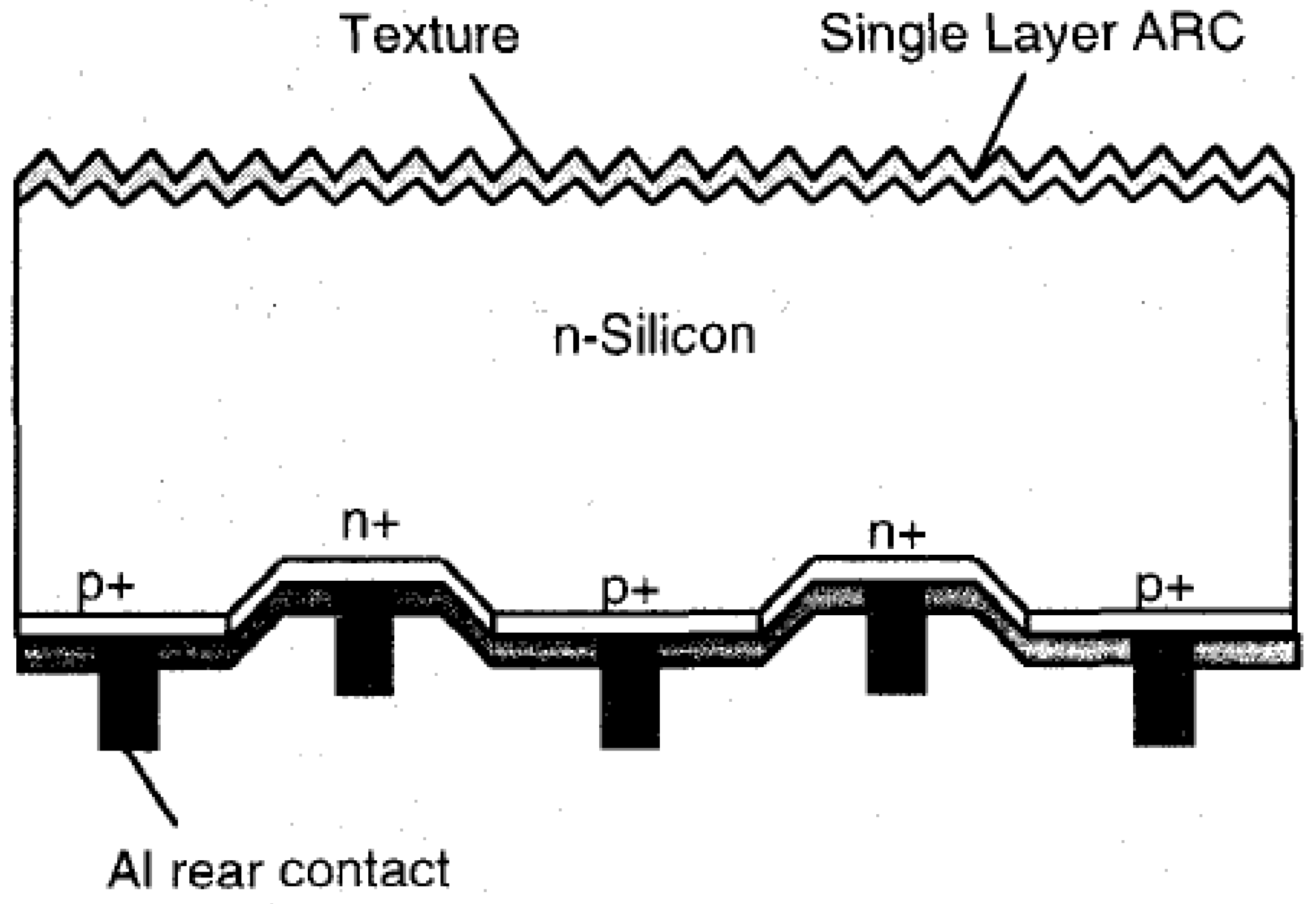
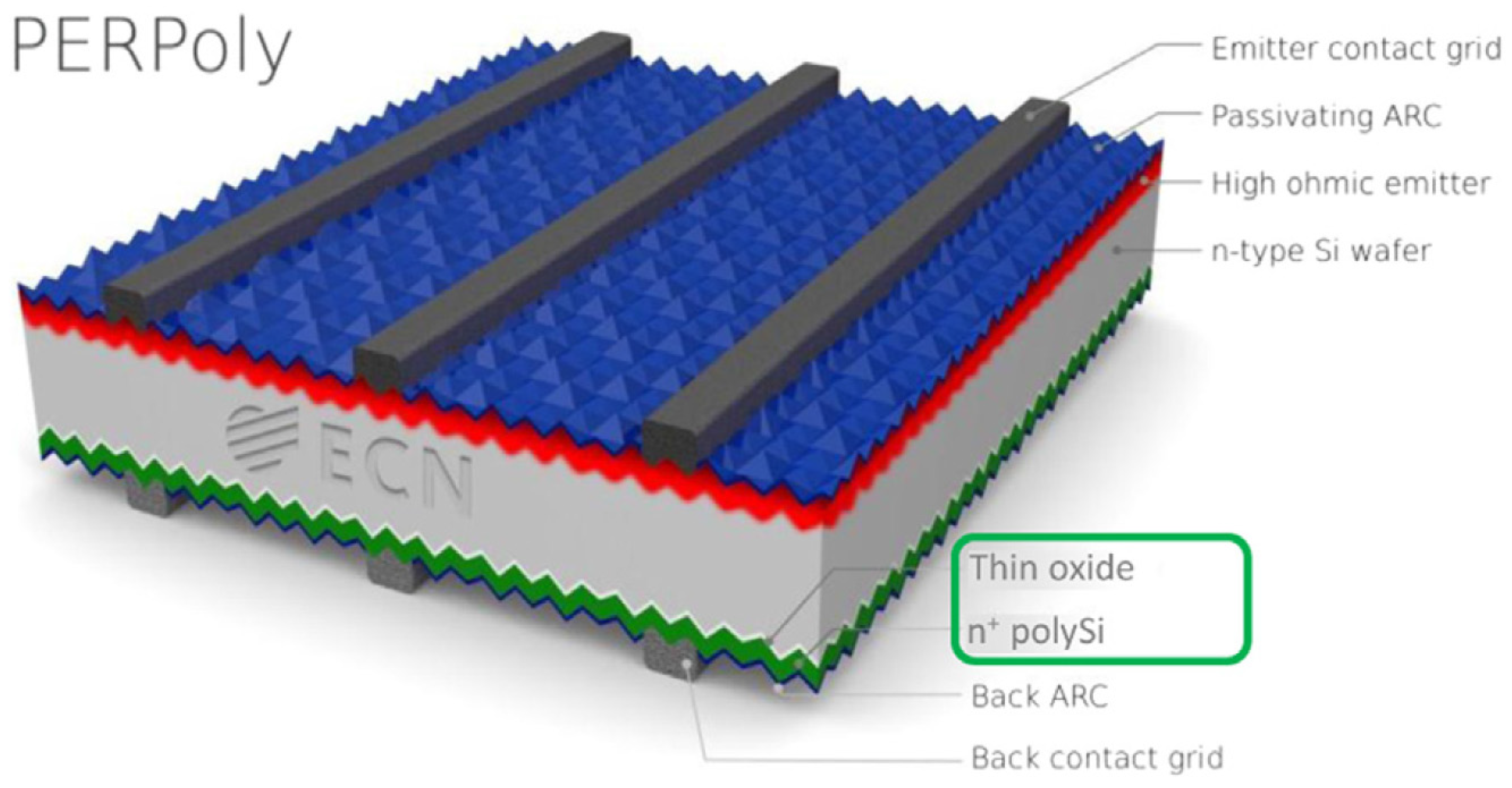
  • The solar cell made with n+ poly-silicon at the rear side with screen-printed metallization yields an optimum 22% efficiency;
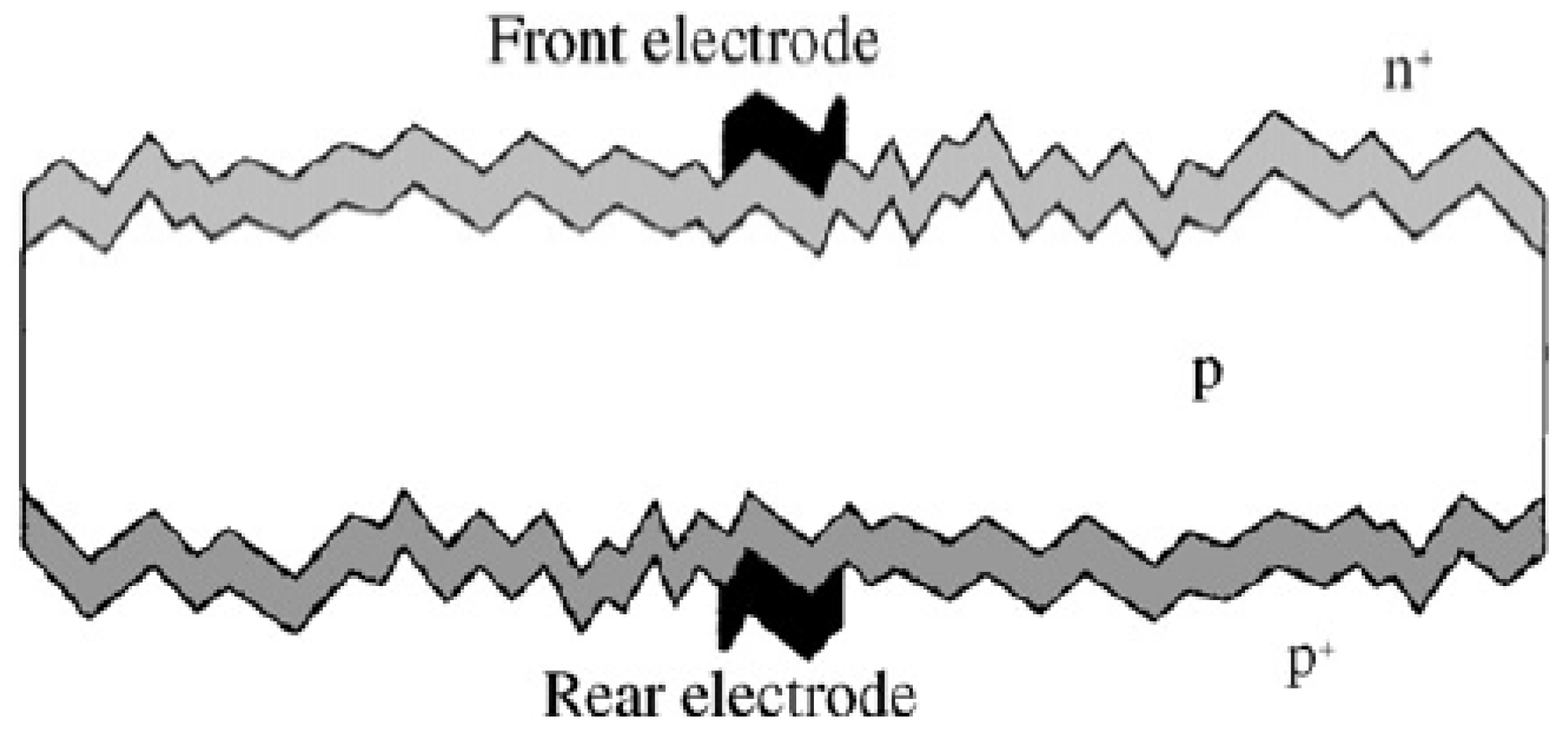
  • A single-crystalline structure used to form triode structure p-n junctions on both sides gives a maximum output on the front side and rear side with an efficiency of 21.3% and 19.8%, respectively;
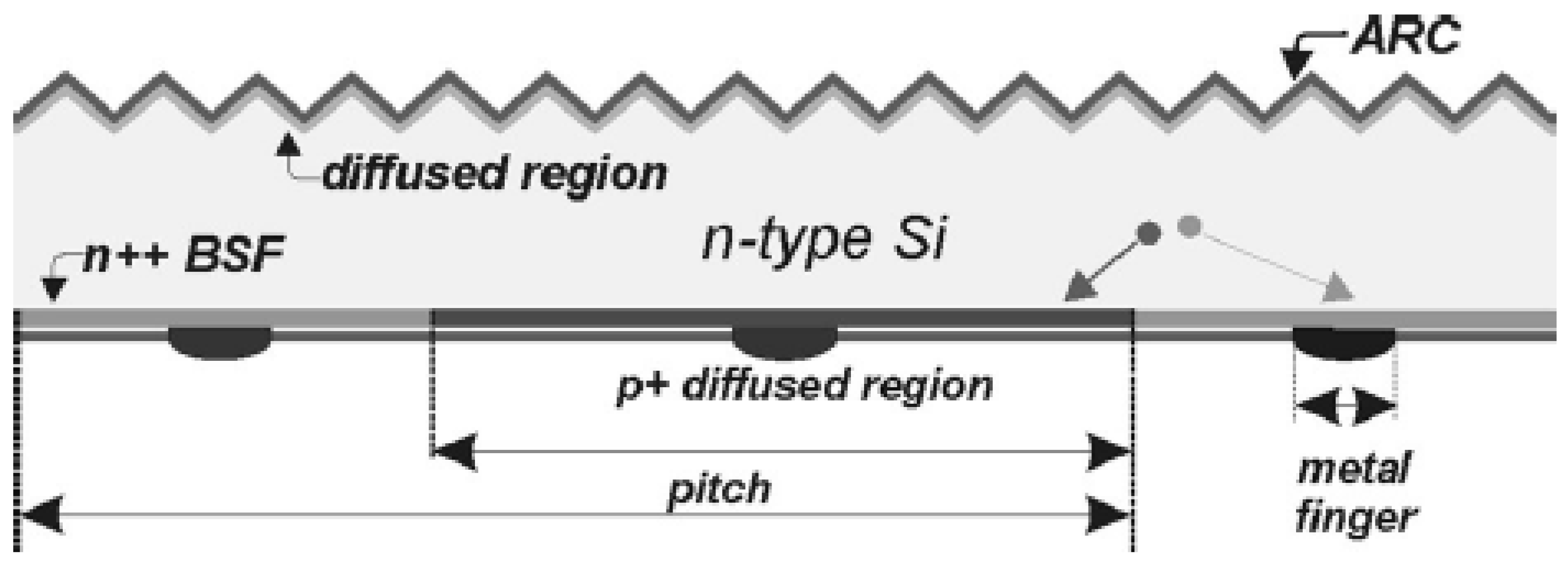
  • Solar panel with CZ-Si wafers made of mono-crystalline n-type delivers an average efficiency of 21% and an FF of 79.1%.

Proposed Future Work

The world is facing the utmost challenges in the fields of energy crisis, pollution, climate change, etc. We should help our society from getting adversely affected by these issues by manufacturing sustainable biodegradable well-designed materials as nature is the master of materials in the world. Consequently, it is essential to produce eco-friendly materials to fit into stringent conditions to be bio-friendly and bio-degradable, avoiding further recycling or disposal. It is proposed to experiment with an organic solar cell in the bifacial solar PV system using organic electronics in the process which deals with small organic molecules or conductive organic polymers for the energy conversion process. Organic BSC with nano polymer material as a carrier transport layer can be investigated [40]. This technology can be integrated into a bifacial PV system incorporating n+ poly-silicon backside contacts through a screen-printing technique to improve the conversion efficiency further.
Over the years, the DSBCB solar cells have exhibited better rear-surface passivation, resulting in improved current and voltage. This was made possible by using a rear n-type layer with much higher sheet resistivity, which addressed the previous limitations. With this new approach, experimental devices achieved fill factors of nearly 82% and open-circuit voltages of around 670 mV. Even without texturing, anti-reflection coatings, light trapping, or rear reflectors, the float-zone material attained efficiencies ranging from 17% to 18%. In the short and medium term, silicon is currently the leading choice as a substrate for bifacial technology under cell substrate. Further research is required to establish a standard thickness for the substrate. For light trapping, texturing in the rear side is included for only bifacial cells. Co-doping and ion implantation in cell thermal processing can serve as a viable alternative to prevent the need for additional thermal processing steps. Generally, the power density per unit area can be boosted by several tens of percentage points when using bifacial PV, as opposed to monofacial PV, particularly when favorable albedo conditions are present.

Author Contributions

Conceptualization, all authors; Formal analysis, M.V., A.M.M. and M.P.; Investigation M.V. and G.R.; Methodology, M.V., A.M.M. and M.P.; Supervision, G.R.; Writing—original draft, M.V., A.M.M. and M.P.; Writing—review and editing, R.S. All authors have read and agreed to the published version of the manuscript.

Funding

This research received no external funding.

Data Availability Statement

Data sharing not applicable.

Conflicts of Interest

The authors declare no conflict of interest.

Abbreviations

PVPhotovoltaic
BSCBifacial Solar Cell
BSPBifacial Solar panel
MSPMonofacial Solar panel
OBCOpaque Back Contact
BSFBack Surface Field
DLARCDouble-Layer Anti-Reflective Coating
SLARCSingle-Layer Anti-Reflective Coating
SiSilicon
FZFloat-Zone
PECVDPlasma-Enhanced Chemical Vapour Deposition
AlAluminum
2XCCM2XCusp-Concentrated Module
BSFBack Surface Field
CZCzochralski
B3Bifacial Boron Back-Surface Field Cell
V(OC)Open-Circuit Voltage
IscShort-Circuit Current
JSCShort-Circuit Current Density
FFFill Factor
PERTPassivated Emitter Rear Totally Diffused
TXTextures
TBCBifacial Transparent Back Contact
LIDLight-Induced Degradation
TCOTransparent Conductive Oxide

References

  1. Press Information Bureau Government of India Home Page. Available online: https://www.pib.gov.in/PressReleasePage.aspx?PRID=1861929 (accessed on 24 September 2022).
  2. Mori, H. Radiation Energy Transducing Device. U.S. Patent No. 3,278,811, 3 October 1966. [Google Scholar]
  3. Cuevas, A.; Luque, A.; Eguren, J.; Del Alamo, J. High efficiency bifacial back surface field solar cells. Sol. Cells 1981, 3, 337–340. [Google Scholar] [CrossRef]
  4. Cuevas, A.; Luque, A.; Eguren, J.; Del Alamo, J. 50 Per cent more output power from an albedo-collecting flat panel using bifacial solar cells. Sol. Energy 1982, 29, 419–420. [Google Scholar] [CrossRef]
  5. Untila, G.G.; Kost, T.N.; Chebotareva, A.B. Bifacial 8.3%/5.4% front/rear efficiency ZnO:Al/n-Si heterojunction solar cell produced by spray pyrolysis. Sol. Energy 2016, 17, 184–197. [Google Scholar] [CrossRef]
  6. Untila, G.G.; Kost, T.N.; Chebotareva, A.B.; Zaks, M.B.; Sitnikov, A.M.; Solodukha, O.I.; Shvarts, M.Z. Concentrator bifacial Ag-free LGCells. Sol. Energy 2014, 106, 88–94. [Google Scholar] [CrossRef]
  7. Untila, G.G.; Kost, T.N.; Chebotareva, A.B. Multi-wire metallization for solar cells: Contact resistivity of the interface between the wires and In2O3:Sn, In2O3:F and ZnO:Al layers. Sol. Energy 2017, 142, 330–339. [Google Scholar] [CrossRef]
  8. Untila, G.G.; Kost, T.N.; Chebotareva, A.B.; Stepanov, A.S.; Zaks, M.B.; Sitnikov, A.M.; Solodukha, O.I. Passivation of boron-doped p+-Si emitters in the (p+nn+) Si solar cell structure with AlOx grown by ultrasonic spray pyrolysis. Sol. Energy 2013, 98, 440–447. [Google Scholar] [CrossRef]
  9. Yang, L.; Ye, Q.H.; Ebong, A.; Song, W.T.; Zhang, G.J.; Wang, J.X.; Ma, Y. High efficiency screen printed bifacial solar cells on mono crystalline CZ silicon. Prog. Photovolt. Res. Appl. 2011, 19, 275–279. [Google Scholar] [CrossRef]
  10. Hubner, A.; Aberle, A.; Hezel, R. Temperature behavior of monofacial and bifacial silicon solar cells. In Proceedings of the Photovoltaic Specialists Conference, Anaheim, CA, USA, 29 September–3 October 1997; pp. 223–226. [Google Scholar]
  11. Hubner, A.; Aberle, A.G.; Hezel, R. Cost-effective bifacial silicon solar cells with 19% front and 18% rear efficiency. In Proceedings of the Photovoltaic Specialists Conference, Anaheim, CA, USA, 29 September–3 October 1997; pp. 489–492. [Google Scholar]
  12. Ortabasi, U. Performance of a 2X Cusp Concentrator PV Module Using Bifacial Solar Cells; (No. CONF-970953--); Institute of Electrical and Electronics Engineers Inc.: Piscataway, NJ, USA, 1997. [Google Scholar]
  13. Zhou, C.Z.; Verlinden, P.J.; Crane, R.A.; Swanson, R.M.; Sinton, R.A. 21.9% efficient silicon bifacial solar cells. In Proceedings of the Photovoltaic Specialists Conference, Anaheim, CA, USA, 29 September–3 October 1997; pp. 287–290. [Google Scholar]
  14. Ohtsuka, H.; Sakamoto, M.; Tsutsui, K.; Yazawa, Y. Bifacial silicon solar cells with 21.3% front efficiency and 19.8% rear efficiency. Prog. Photovolt. Res. Appl. 2000, 8, 385–390. [Google Scholar] [CrossRef]
  15. Kranzl, A.; Kopecek, R.; Peter, K.; Fath, P. Bifacial solar cells on multi-crystalline silicon with boron BSF and open rear contact. In Proceedings of the IEEE 4th World Conference on Photovoltaic Energy Conference, Waikoloa, HI, USA, 7–12 May 2006; Volume 1, pp. 968–971. [Google Scholar]
  16. Ohtsuka, H.; Sakamoto, M.; Koyama, M.; Muramatsu, S.; Yazawa, Y.; Warabisako, T.; Saitoh, T. Effect of light degradation on bifacial Si solar cells. Sol. Energy Mater. Sol. Cells 2001, 66, 51–59. [Google Scholar] [CrossRef]
  17. Uematsu, T.; Tsutsui, K.; Yazawa, Y.; Warabisako, T.; Araki, I.; Eguchi, Y.; Joge, T. Development of bifacial PV cells for new applications of flat-plate modules. Sol. Energy Mater. Sol. Cells 2003, 75, 557–566. [Google Scholar] [CrossRef]
  18. Böscke, T.S.; Kania, D.; Helbig, A.; Schöllhorn, C.; Dupke, M.; Sadler, P.; Jesswein, R. Bifacial n-type cells with >20% front-side efficiency for industrial production. IEEE J. Photovolt. 2013, 3, 674–677. [Google Scholar] [CrossRef]
  19. Galbiati, G.; Mihailetchi, V.D.; Roescu, R.; Halm, A.; Koduvelikulathu, L.J.; Kopecek, R.; Libal, J. Large-area back-contact back-junction solar cell with efficiency exceeding 21%. IEEE J. Photovolt. 2013, 3, 560–565. [Google Scholar] [CrossRef]
  20. Moehlecke, A.; Febras, F.S.; Zanesco, I. Electrical performance analysis of PV modules with bifacial silicon solar cells and white diffuse reflector. Sol. Energy 2013, 96, 253–262. [Google Scholar] [CrossRef]
  21. Chang, H.C.; Huang, C.J.; Hsieh, P.T.; Mo, W.C.; Yu, S.H.; Li, C.C. Improvement on industrial n-type bifacial solar cell with >20.6% efficiency. Energy Procedia 2014, 55, 643–648. [Google Scholar] [CrossRef]
  22. Madon, F.; Einhaus, R.; Degoulange, J.; Comparotto, C.; Galbiati, G.; Wefringhaus, E. Bifacial NICE Modules from High Efficiency n-type BiSoN Solar Cells. Energy Procedia 2015, 77, 382–385. [Google Scholar] [CrossRef]
  23. Khanal, R.R.; Phillips, A.B.; Song, Z.; Xie, Y.; Mahabaduge, H.P.; Dorogi, M.D.; Zafar, S.; Faykosh, G.T.; Heben, M.J. Substrate configuration, bifacial CdTe solar cells grown directly on transparent single wall carbon nanotube back contacts. Sol. Energy Mater. Sol. Cells 2016, 157, 35–41. [Google Scholar] [CrossRef]
  24. Myong, S.Y.; Jeon, S.W. Efficient outdoor performance of esthetic bifacial a-Si: H semi-transparent PV modules. Appl. Energy 2016, 164, 312–320. [Google Scholar] [CrossRef]
  25. Sahin, G.; Barro, F.I.; Sané, M.; Honadia, P.A.A.; Kocyigit, A.; Kerimli, G. Performance of conversion efficiency of a bifacial silicon solar cell with particle irradiation. Chin. J. Phys. 2016, 55, 203–210. [Google Scholar] [CrossRef]
  26. Stodolny, M.K.; Lenes, M.; Wu, Y.; Janssen, G.J.M.; Romijn, I.G.; Luchies, J.R.M.; Geerligs, L.J. n-Type polysilicon passivating contact for industrial bifacial n-type solar cells. Sol. Energy Mater. Sol. Cells 2016, 158, 24–28. [Google Scholar] [CrossRef]
  27. Yu, B.; Song, D.; Sun, Z.; Liu, K.; Zhang, Y.; Rong, D.; Liu, L. A study on electrical performance of N-type bifacial PV modules. Sol. Energy 2016, 137, 129–133. [Google Scholar] [CrossRef]
  28. Wei, Q.; Wu, C.; Liu, X.; Zhang, S.; Qian, F.; Lu, J.; Ni, P. The Glass-glass Module Using n-type Bifacial Solar Cell with PERT Structure and its Performance. Energy Procedia 2016, 92, 750–754. [Google Scholar] [CrossRef]
  29. Chebotareva, A.B.; Untila, G.G.; Kost, T.N.; Stepanov, A.S.; Salazkin, S.N.; Shaposhnikova, V.V. Transparent conductive polymers for laminated multi-wire metallization of bifacial concentrator crystalline silicon solar cells with TCO layers. Sol. Energy Mater. Sol. Cells 2017, 165, 1–8. [Google Scholar] [CrossRef]
  30. Shi, Y.; Ma, R.; Wang, X.; Liu, T.; Li, Y.; Fu, S.; Yang, K.; Wang, Y.; Yu, C.; Jiao, L. Influence of fluorine substitution on the photovoltaic performance of wide band gap polymer donors for polymer solar cells. ACS Appl. Mater. Interfaces 2022, 14, 5740–5749. [Google Scholar] [CrossRef]
  31. Ingenito, A.; Allebé, C.; Libraro, S.; Ballif, C.; Paviet-Salomon, B.; Nicolay, S.; Leon, J.J.D. 22.8% full-area bifacial n-PERT solar cells with rear side sputtered poly-Si (n) passivating contact. Sol. Energy Mater. Sol. Cells 2023, 249, 112043. [Google Scholar] [CrossRef]
  32. Chen, C.J.; Chandel, A.; Thakur, D.; Wu, J.R.; Chiang, S.E.; Zeng, G.S.; Shen, J.L.; Chen, S.H.; Chang, S.H. Ag modified bathocuproine: ZnO nanoparticles electron buffer layer based bifacial inverted-type perovskite solar cells. Org. Electron. 2021, 92, 106110. [Google Scholar] [CrossRef]
  33. Ma, S.; Tang, H.B.; Li, Z.P.; Kong, X.Y.; Shen, W.Z. Application of SiOxNy films in industrial bifacial PERC solar cells. Sol. Energy Mater. Sol. Cells 2021, 230, 111199. [Google Scholar] [CrossRef]
  34. Pham, D.P.; Lee, S.; Kim, Y.; Yi, J. Band-offset reduction for effective hole carrier collection in bifacial silicon heterojunction solar cells. J. Phys. Chem. Solids 2021, 154, 110059. [Google Scholar] [CrossRef]
  35. Chebotareva, A.B.; Untila, G.G.; Kost, T.N.; Stepanov, A.S.; Salazkin, S.N.; Shaposhnikova, V.V. Bifacial IFO/(n+ pp+) Cz-Si/ITO silicon solar cell with advanced Ag-free multi-wire metallization attached to TCO layers by transparent conductive PAES copolymers. Sol. Energy 2018, 164, 292–300. [Google Scholar] [CrossRef]
  36. Untila, G.G.; Kost, T.N.; Chebotareva, A.B. Bifacial IFO/(n+ pp+) Cz-Si/ITO solar cells with full-area Al-alloyed BSF and Ag-free multi-wire metallization suitable for low-concentration systems. Sol. Energy 2019, 193, 992–1001. [Google Scholar] [CrossRef]
  37. Liu, H.; Lang, R.; Jiang, S.; Lu, W.; Zhang, W.; Feng, L.; Yu, W. Bifacial semitransparent perovskite solar cells with MoOx/Cu/Ag/MoOx multilayer transparent electrode. Sol. Energy 2021, 228, 290–298. [Google Scholar] [CrossRef]
  38. Ma, J.; Song, Y.; Qiao, S.; Liu, D.; Ding, Z.; Kopecek, R.; Chen, J.; Zhang, C.; Chen, M. Design, realization and loss analysis of efficient low-cost large-area bifacial interdigitated-back-contact solar cells with front floating emitter. Sol. Energy Mater. Sol. Cells 2022, 235, 111466. [Google Scholar] [CrossRef]
  39. Nishimura, T.; Chantana, J.; Mavlonov, A.; Kawano, Y.; Masuda, T.; Minemoto, T. Device design for high-performance bifacial Cu (In, Ga) Se2 solar cells under front and rear illuminations. Sol. Energy 2021, 218, 76–84. [Google Scholar] [CrossRef]
  40. Çetinkaya, Ç. Efficient and high-bifacial CdTe-based solar cell enabled by functional designed dielectric/metal/dielectric transparent top contact via light management engineering. Opt. Mater. 2022, 133, 113003. [Google Scholar] [CrossRef]
Figure 1. Cross-section view of standard n-type and p-type bifacial crystalline Si solar cells [9].
Energies 16 03605 g001
Figure 2. Schematic representation of the investigated Si BSC [10].
Energies 16 03605 g002
Figure 3. Schematic representation of the investigated BSC [11].
Energies 16 03605 g003
Figure 4. Cross-section of assembled laminate [12].
Energies 16 03605 g004
Figure 5. Schematic representation of a rear-contact bifacial cell [13].
Energies 16 03605 g005
Figure 6. Schematic diagram of a bifacial triode solar cell with bifacial p-n junction cells [14].
Energies 16 03605 g006
Figure 7. Output power measured over one day in mid-April [15].
Energies 16 03605 g007
Figure 8. The cross-section of fabricated BSC: (a) Rear-Floating Emitter (RFE) cell with random texture and (b) triode cell with inverted pyramids [16].
Energies 16 03605 g008
Figure 9. Cross-section of B3 cell [17].
Energies 16 03605 g009
Figure 10. Schematic cross-section of our bifacial nPERT-Cell with screen-printed metallization [18].
Energies 16 03605 g010
Figure 11. Cross-section of a ZEBRA cell showing the geometry of the diffused region on the back side. The cell thickness is 150 μm, and the pitch size is 1.4 mm. The front alkaline texture and the optimized anti-reflection SiNx coating layer allow the minimum reflection and the maximum photogeneration current [19].
Energies 16 03605 g011
Figure 12. PV module with bifacial cells and diffuse back reflector [20].
Energies 16 03605 g012
Figure 13. Schematic cross-section of N-type BSC [21].
Energies 16 03605 g013
Figure 14. The electrical energy yield of the TBC a-Si:H semi-transparent PV modules mounted with different h. The ‘‘mea” and ‘‘sim” denote the measured and simulated values, respectively. In x-axis, ‘‘1” is corresponding to January, while ‘‘12” to December. The solid lines are eye guides [24].
Energies 16 03605 g014
Figure 15. Bifacial Si solar cell [25].
Energies 16 03605 g015
Figure 16. Conversion efficiency for monofacial and BSC versus particle fluence (H = 0.02 cm, Sb = 10.2 cm s−1, Nb = 10.17 cm−3) [25].
Energies 16 03605 g016
Figure 17. Schematic drawing of the bifacial n-type solar cell design featuring n-polySi/SiOx contacts, named PERPoly (Passivated Emitter and Rear PolySi) [26].
Energies 16 03605 g017
Figure 18. Roadmap towards 22% PERC Poly cell [26].
Energies 16 03605 g018
Figure 19. A cross-section of a N-type BSC [27].
Energies 16 03605 g019
Figure 20. Comparison of energy output between a bifacial module and a regular module on a sunny day [27].
Energies 16 03605 g020
Figure 21. Comparison of energy output between a bifacial module and a regular module on a cloudy day [27].
Energies 16 03605 g021
Figure 22. Schematic of a bifacial TCP-containing LGCell: sections (a) along and (b) across the wires. The cell in picture (a) is not encapsulated [29]. * round soldered copper wires 60 μm. ** transparent conductive polymer, 20 μm thick. *** polypropylene lamination film, 40-μm-thick.
Energies 16 03605 g022
Figure 23. Efficiency as a function of concentration ratio for LGCell #P50 and reference LGCell under front and rear illumination [29].
Energies 16 03605 g023
Figure 24. Generation process of (a) monofacial and (b) bifacial solar cells.
Energies 16 03605 g024
Table 1. Different research works made in bifacial solar PV.
S.No.Author NameTesting PlaceMaterialEfficiency (%)Fill Factor
FrontRearFrontRear
1Andreas Hubner et al. [10]Emmerthal, GermanyCombined PECVD Si nitride film with simple alloyed Al BSF19.416.581.881.2
2Ugur ortabasi [11]San Diego2XCusp Concentrated Module (2XCCM) using RFSC1514--
3C.Z. Zhou et.al [12]San Jose, USAFZ n-type Si wafers20.6610.5479.680.5
4H. Ohtsuka [16]TokyoTriode structure with p-n junctions on both sides into single-crystalline bifacial Si solar cells21.319.881.681.3
5Kranzl et al. [15]Konstanz, GermanyBoron-BSF16.112.475.674.8
6H. Ohtsuka et al. [16]Central Research Laboratory, Hitachi, Tokyo, JapanBifacial type rear-floating-emitter solar cells and triode solar cells using four types of wafers, Boron-doped Cz (Cz(B)), Magnetic-field-applied Cz (MCZ), Gallium-doped CZ (CZ(ga)) and FZ wafers20.418.979.780.3
7Uematsu et al. [17]Central Research Laboratory, Hitachi, Tokyo, JapanCell which denotes bifacial boron BSF- soar grade (SoG) CZ Si substrate1510.5--
8T.S. Boscke et al. [18]Bosch Solar Energy, GermanyHomogenous boron front side emitter and phosphorous back surface field20.1319.86--
9Guiseppe galbiati et al. [19]Solar Energy Research Center, GermanyMonocrystalline n-type CZ-Si wafersAvg—21.0 Avg—79.1
10Moehlecke et al. [20]BrazilP+n++ BSC14.213.773.175.7
11Boscke et al. [18]Taiwan6 inch n-type Cz Si wafers20.63-81.3-
12Madon et al. [22]ISCKonstanz
test site in El Gouna, Egypt (27°N latitude)
Bifacial glass/glass NICE modules, using n-type BiSoN solar cellsAverage bifaciality factor—88.5-74.977.9
13Rajendra R. Khanal et al. [23]Toledo, USACdTe/cds solar cells in single-cell carbon nanotube substrate without the use of copper6.5-50.4-
14Seung yeop myong et al. [24]Republic of KoreaHydrogenated amorphous Si (a-si:H) semitransparent glass-to-glass PV modulesPerformance ratio = 124.5---
15Stodolny et al. [26]ECN Solar energy, NetherlandsBifacial n-type solar cell with LPCVD n+ polySi backside passivating contacts and fire-through screen-printed metallizationOptimum efficiency = 22---
16Ingenito
et al. [30]
Switzerlandphosphorus-doped polysilicon (polySi(n)) on a thin silicon oxide22.8--
17Chen et al. [31]Taiwaninverted-type perovskite solar cells using ZnO nanoparticles thin film as the buffer layer15.50--
18Ma et al. [32]Republic of Chinabifacial p-Si PERC cells using hydrogenated amorphous silicon oxynitride23.2317.31--
19Duy Phong Pham et al. [33]Republic of KoreaBifacial silicon heterojunction solar cells using an ultra-thin buffer
layer of hydrogenated amorphous silicon oxide
23.680
20Chebotareva et al. [34]RussiaBSC uses transparent conductive
oxide (TCO) layers
18.215.178.479.1
21Untila et al. [35]RussiaBSC uses Al-alloyed17.911.278.177.9
22Hongyan Liu et al. [36]ChinaBifacial perovskite solar cells with MoOx/Cu/Ag/MoOx
transparent multilayer electrode
13.4410.25
23Ma et al. [37]ChinaBSC with front floating emitter22.979.6
24Takahito Nishimura et al. [38]JapanHigh-efficient bifacial CIGSe solar cell21.623.8--
25Çetinkaya et al. [39]TurkeyCdTe-based BSC4.9610.6963.4262.30
Disclaimer/Publisher’s Note: The statements, opinions and data contained in all publications are solely those of the individual author(s) and contributor(s) and not of MDPI and/or the editor(s). MDPI and/or the editor(s) disclaim responsibility for any injury to people or property resulting from any ideas, methods, instructions or products referred to in the content.

