
A High Conversion Ratio DC–DC Boost Converter with Continuous Output Current Using Dual-Current Flows


Abstract
:1. Introduction
1.1. Large Inductor Current
- T = temperature of the inductor
- RL_25C = inductor series resistance at room temperature (25 °C)
- TCCopper = temperature coefficient of copper that is equal to 0.00393
1.2. Pulsating Output Delivery Current
1.3. Limitation of Conversion Gain
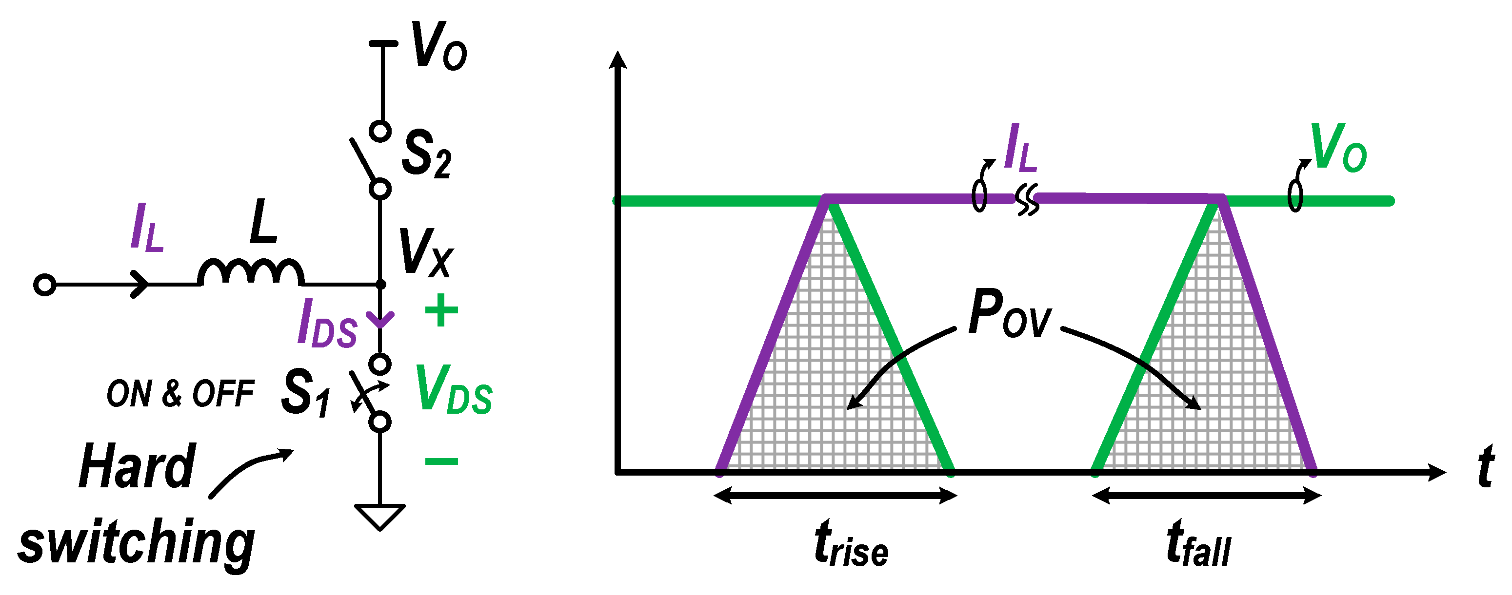
1.4. Large Overlap Loss
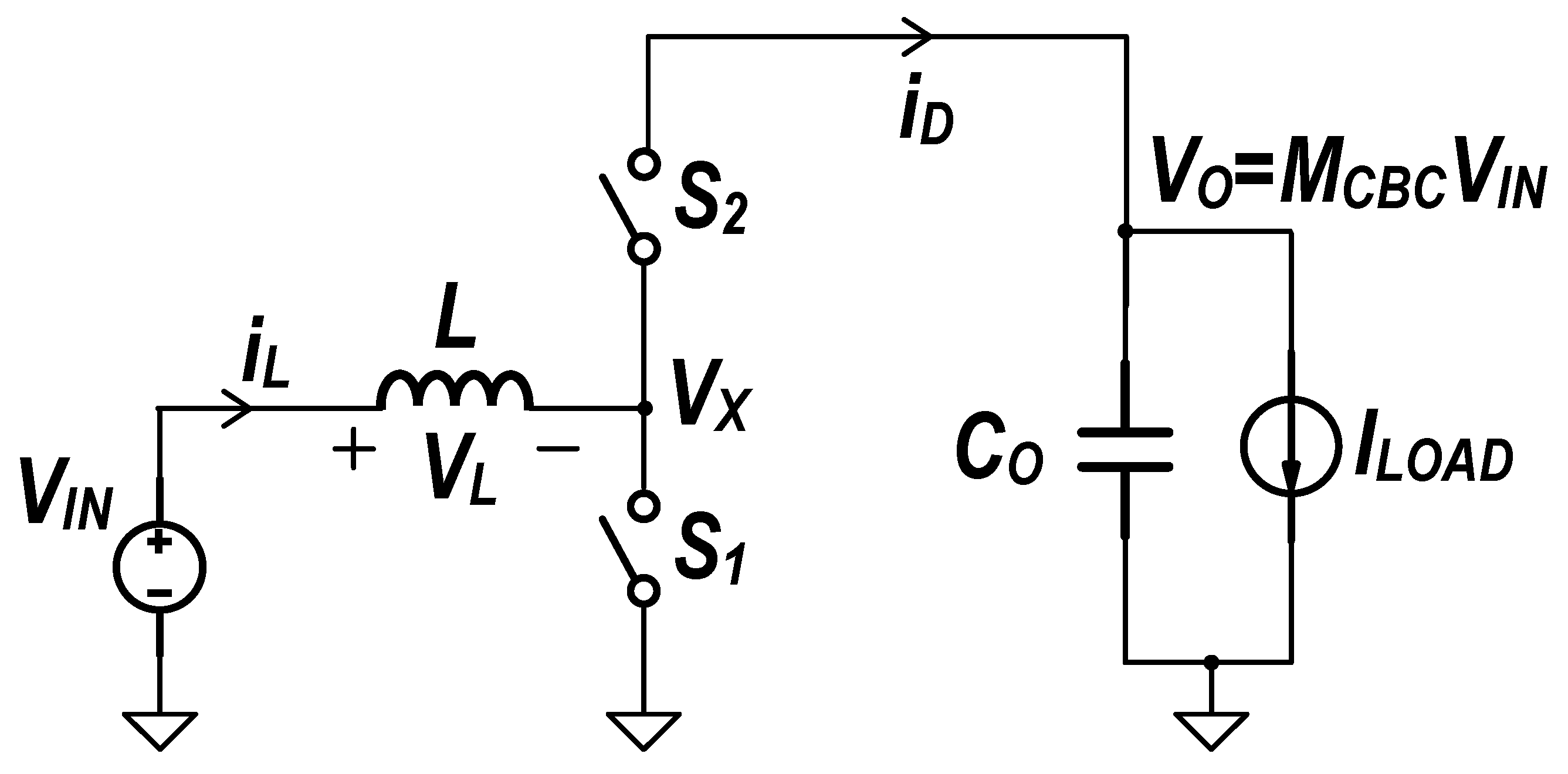
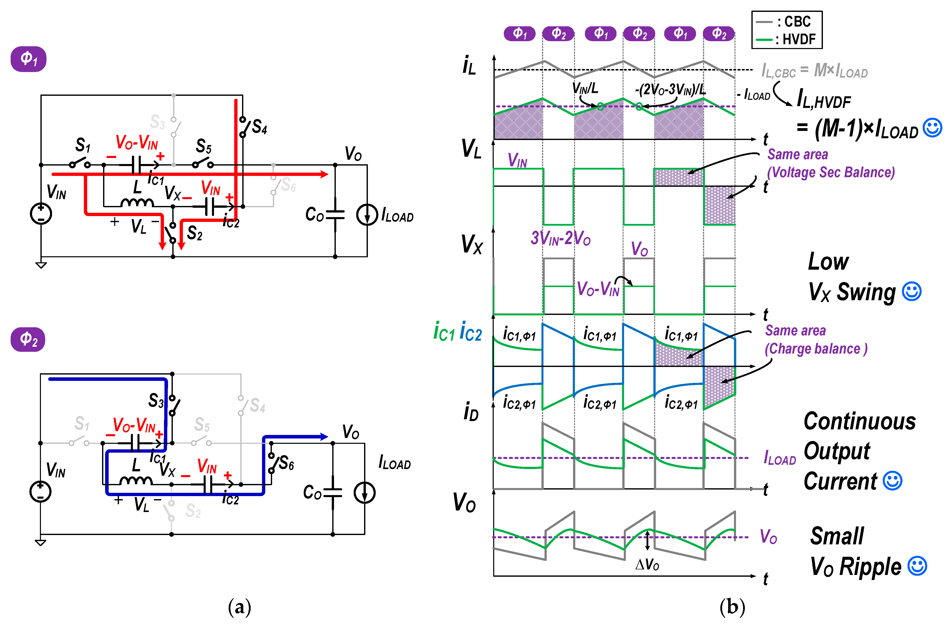
2. High-Voltage Boost Converter with Dual-Current Flows
2.1. Reduced Inductor Current
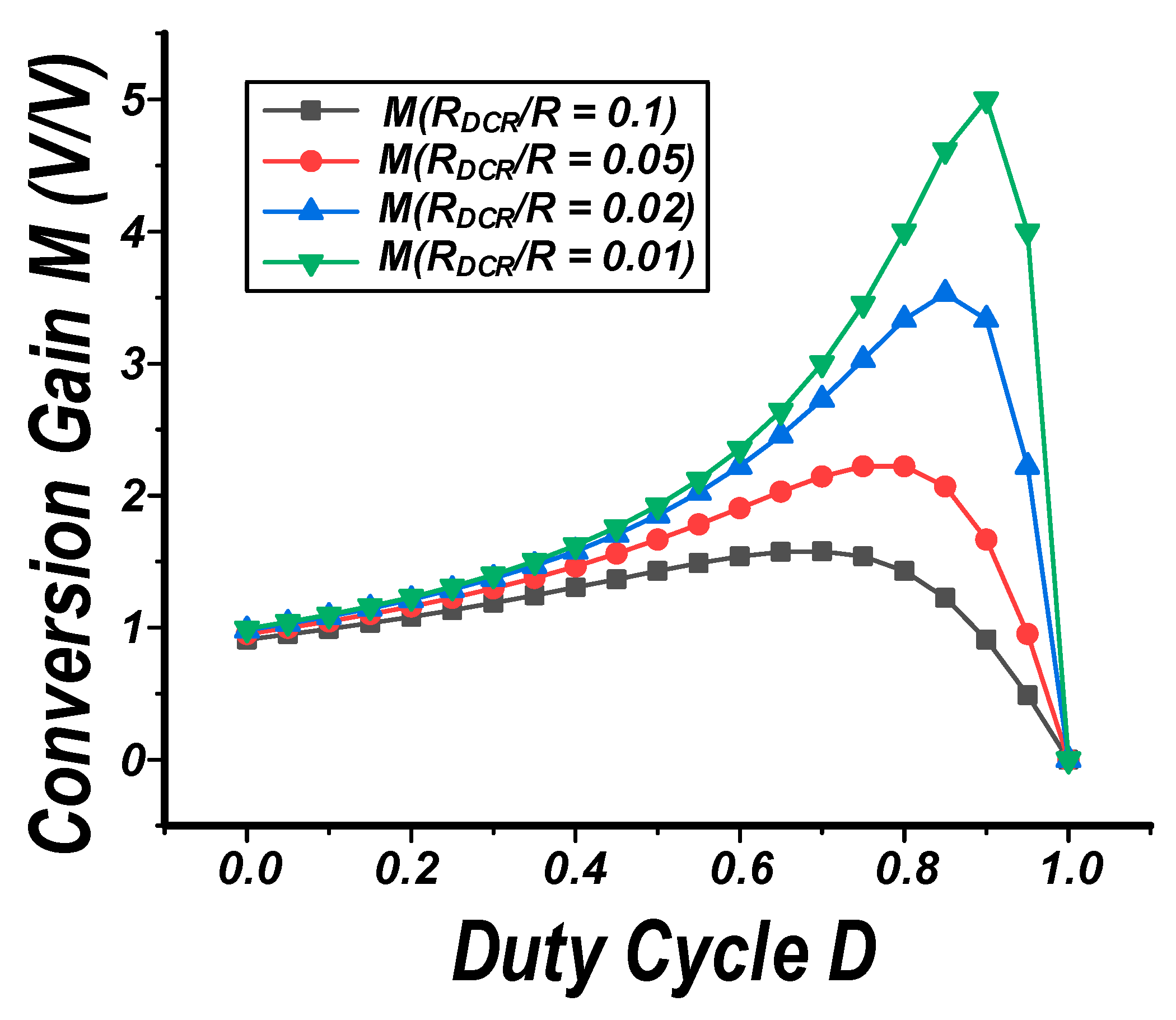
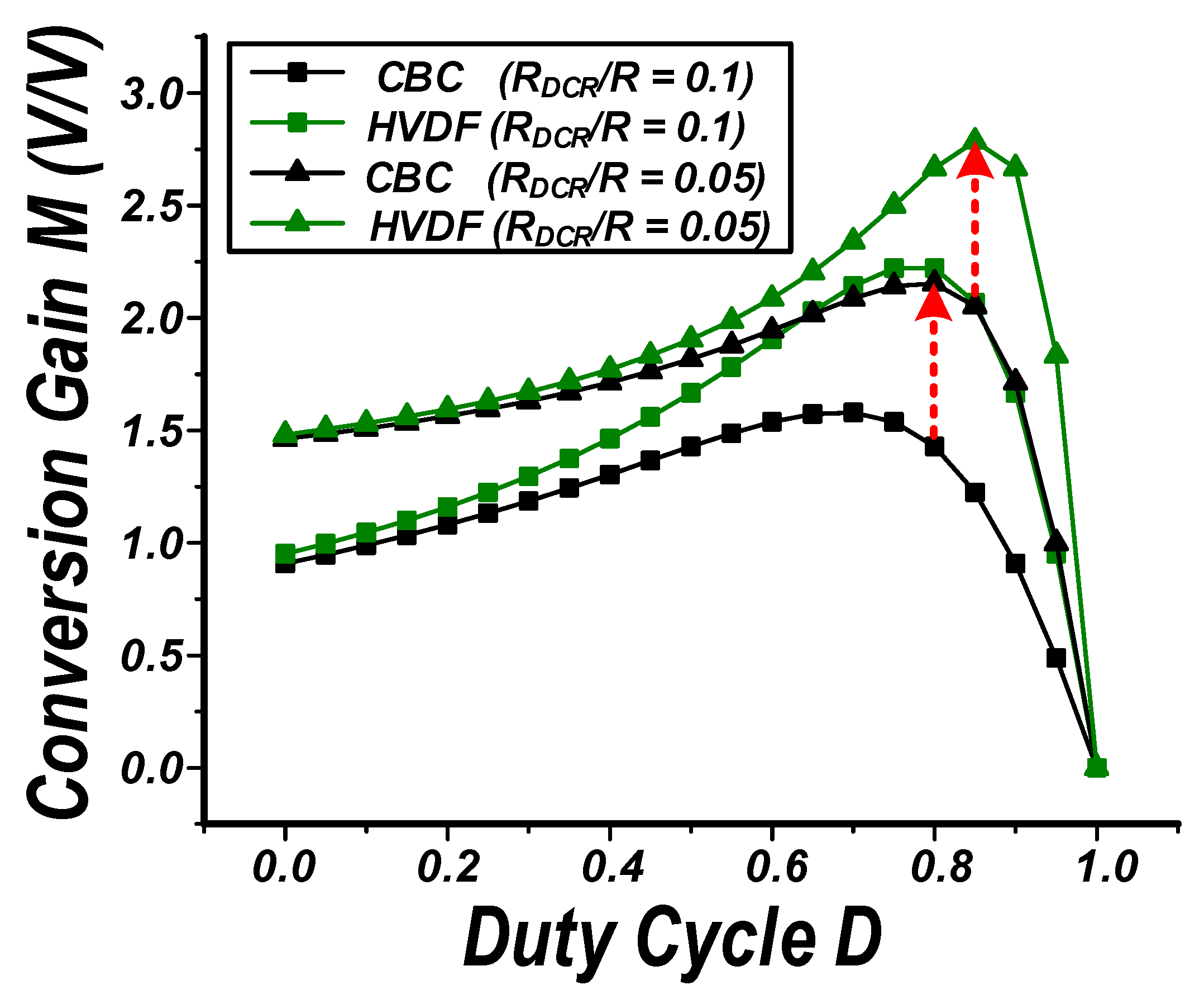
2.2. Alleviated Conversion Gain Limit
2.3. Reduced Overlap Loss
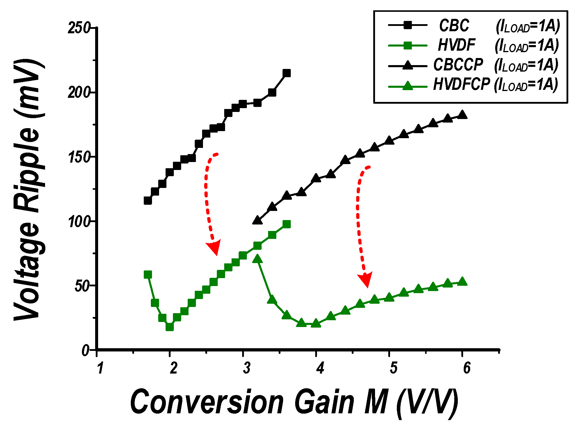
2.4. Small Output Voltage Ripple
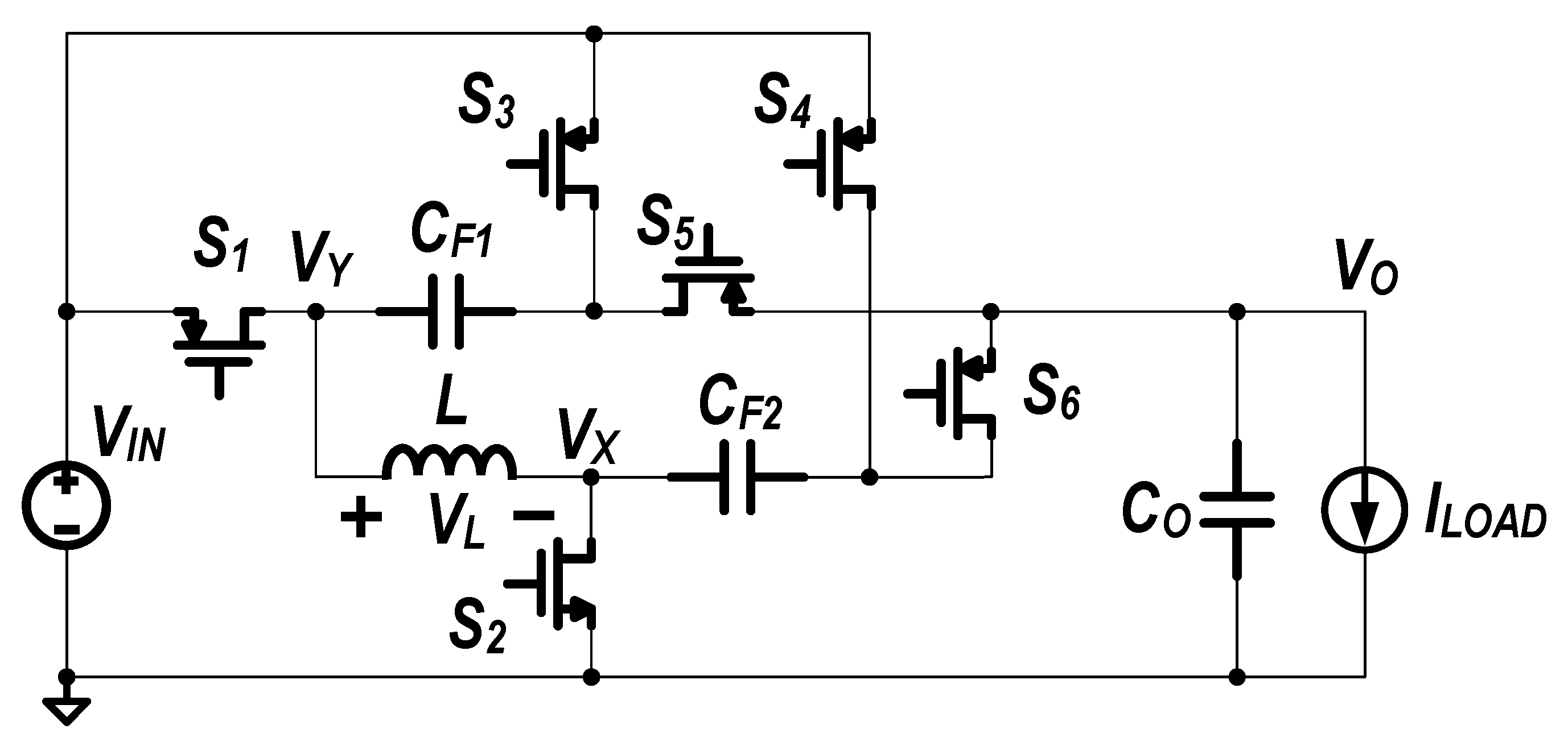
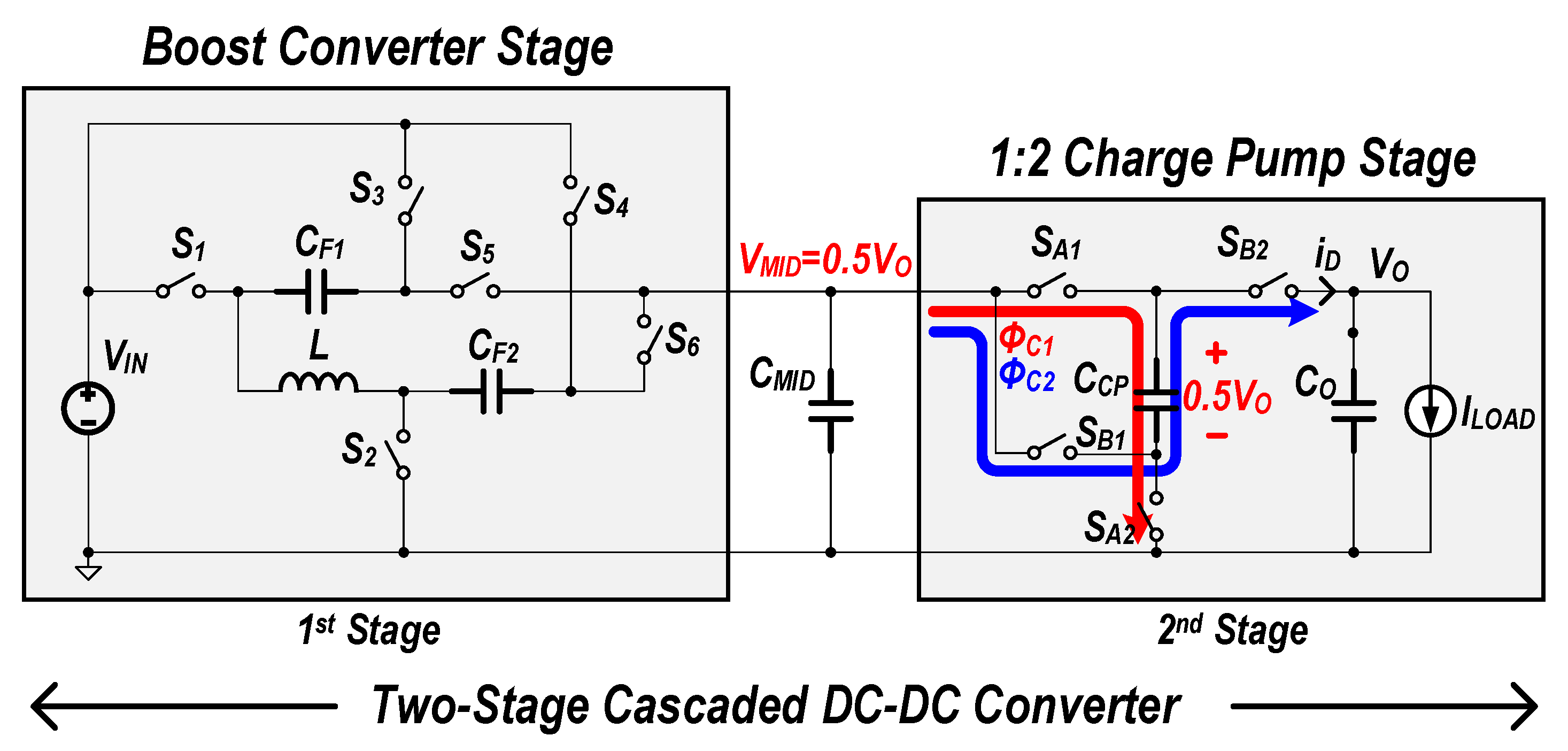
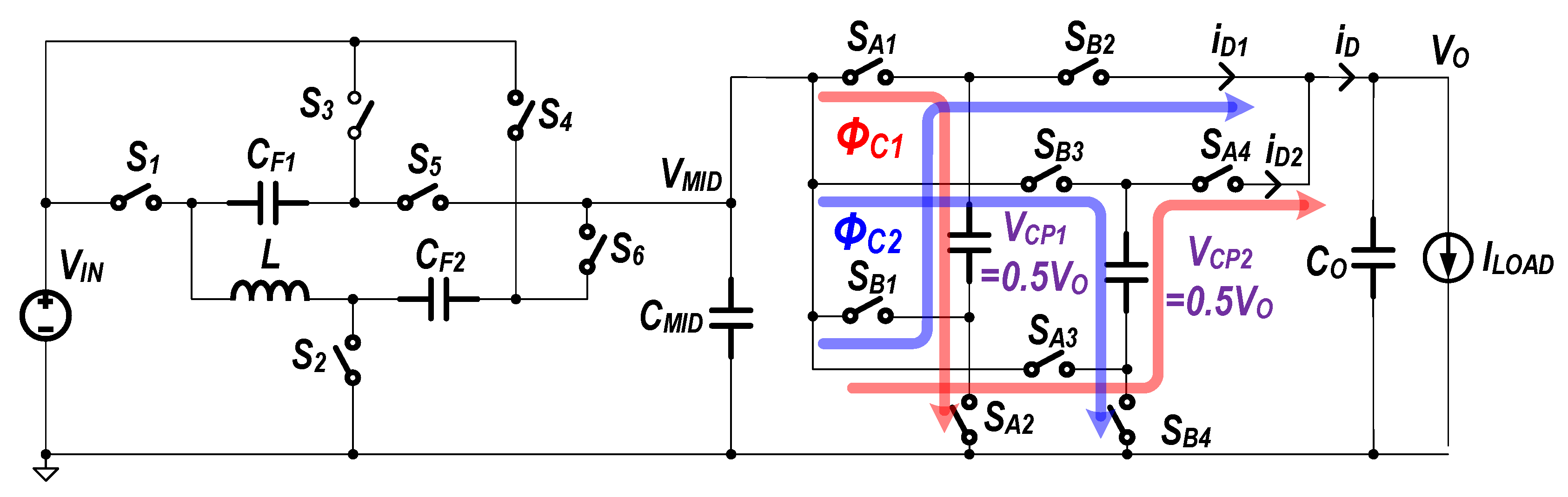
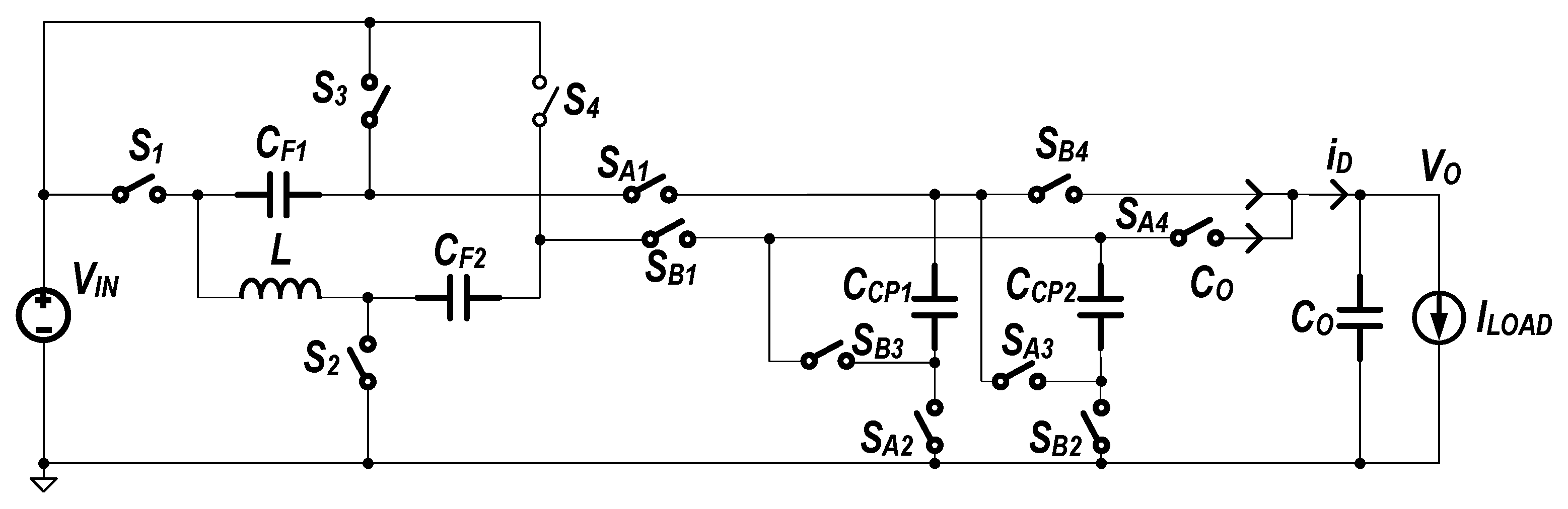
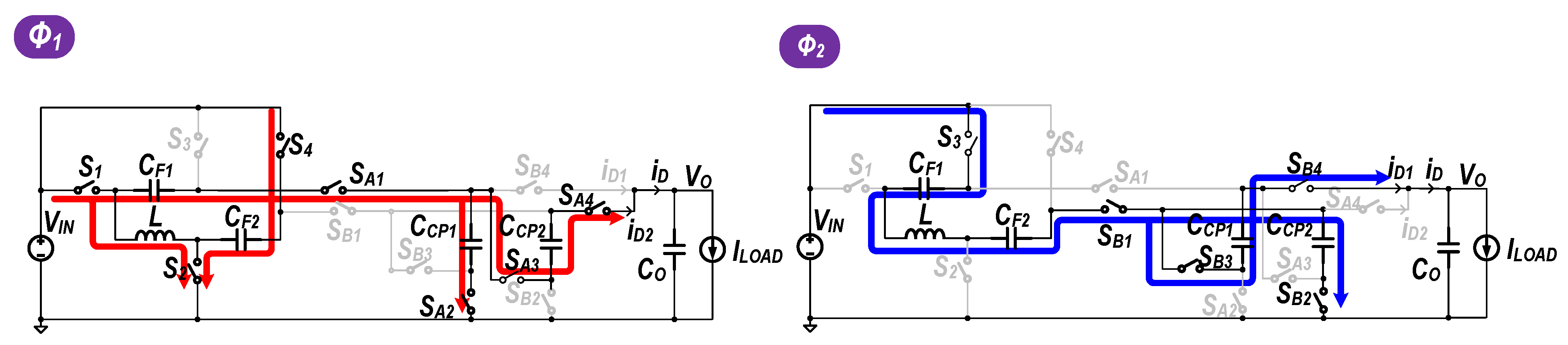
3. High-Voltage Boost Converter with Dual-Current Flows and Time-Interleaved Charge Pump
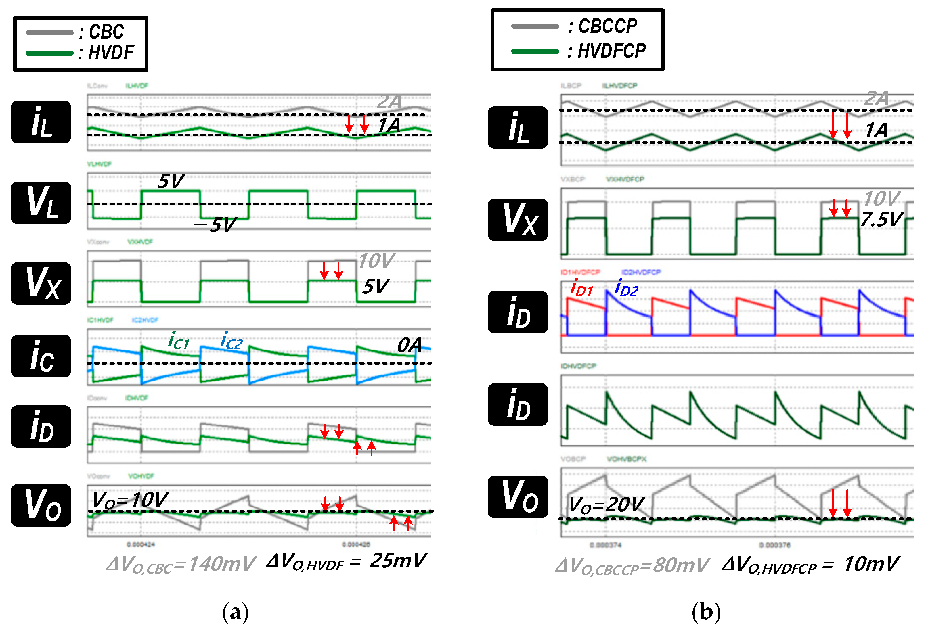
4. Simulation Results and Discussion
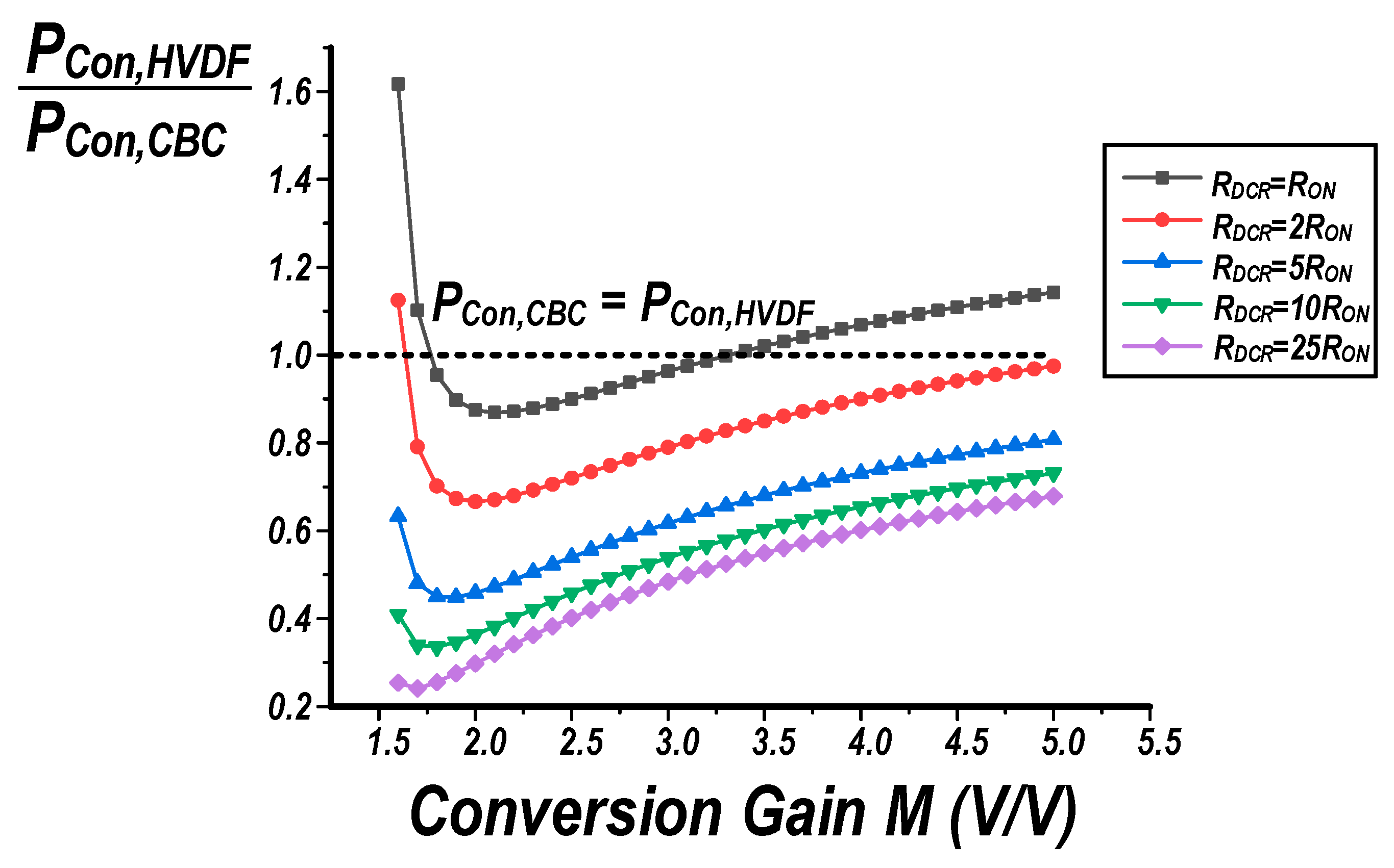
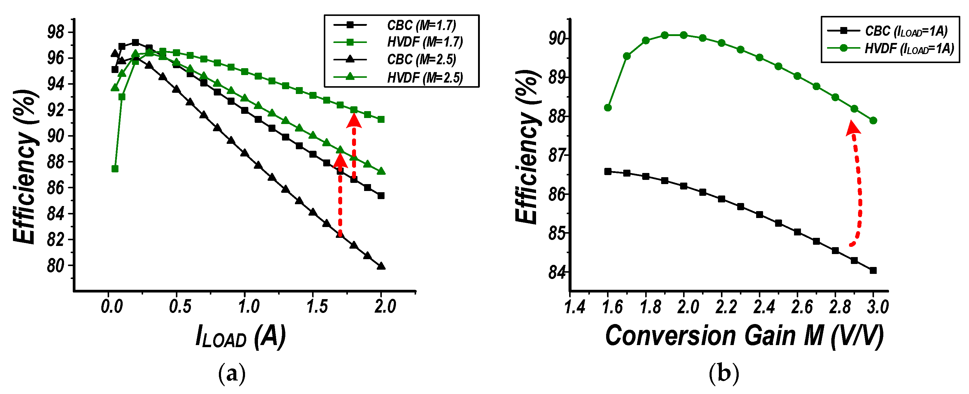
4.1. High-Voltage Boost Converter with Dual-Current Flows
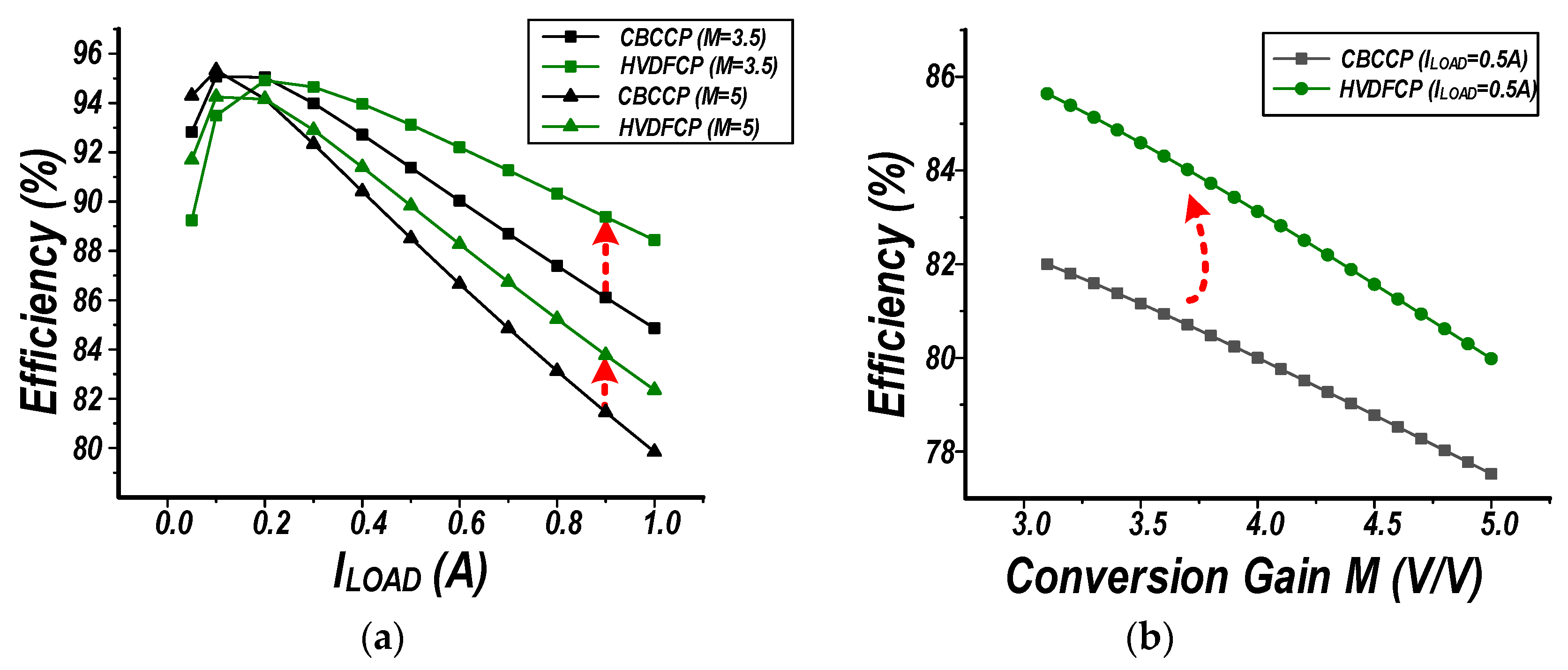
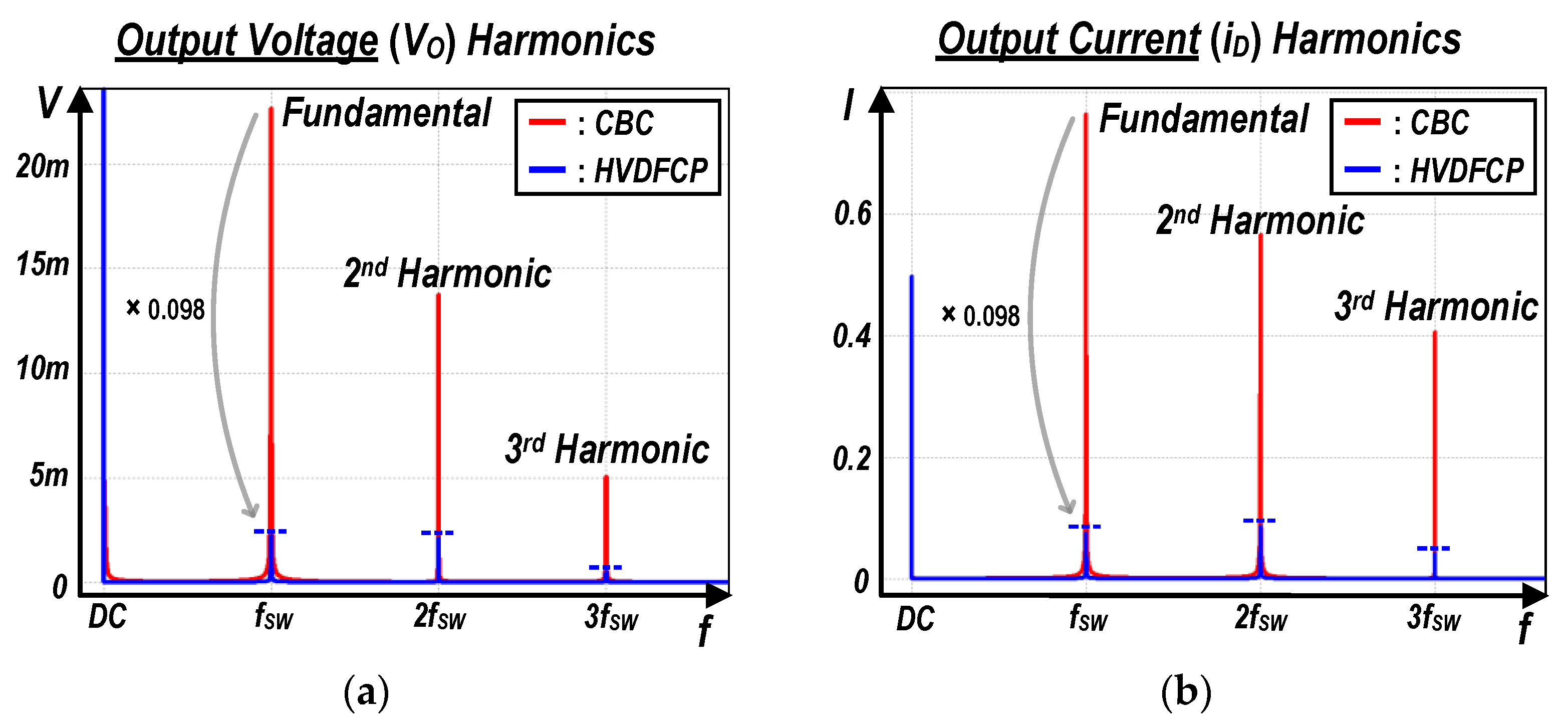
4.2. High-Voltage Boost Converter with Dual-Current Flows and Time-Interleaved Charge Pump
5. Conclusions
Author Contributions
Funding
Data Availability Statement
Conflicts of Interest
References
- Hsieh, C.Y.; Wang, S.J.; Lee, Y.H.; Chen, K.H. LED drivers with PPD compensation for achieving fast transient response. In Proceedings of the 2008 IEEE International Symposium on Circuits and Systems, Seattle, DC, USA, 18–21 May 2008; pp. 2202–2205. [Google Scholar]
- Hsieh, C.; Chen, K. Boost DC-DC Converter with Fast Reference Tracking (FRT) and Charge-Recycling (CR) Techniques for High-Efficiency and Low-Cost LED Driver. IEEE J. Solid-State Circuits 2009, 44, 2568–2580. [Google Scholar] [CrossRef]
- Sulake, N.R.; Venkata, A.K.D.; Choppavarapu, S.B. FPGA Implementation of a Three-Level Boost Converter-fed Seven-Level DC-Link Cascade H-Bridge inverter for Photovoltaic Applications. Electronics 2018, 7, 282. [Google Scholar] [CrossRef]
- Zhu, H.; Liu, D.; Zhang, X.; Qu, F. Reliability of Boost PFC Converters with Improved EMI Filters. Electronics 2018, 7, 413. [Google Scholar] [CrossRef]
- Zhang, R.; Ma, W.; Wang, L.; Hu, M.; Cao, L.; Zhou, H.; Zhang, Y. Line Frequency Instability of One-Cycle-Controlled Boost Power Factor Correction Converter. Electronics 2018, 7, 203. [Google Scholar] [CrossRef]
- Lee, S.; Jeong, Y.; Cho, M.; Kim, J.; Kim, H.; Bang, J.; Shin, S. 30.5 A 95.3% 5V-to-32V Wide Range 3-Level Current Mode Boost Converter with Fully State-based Phase Selection Achieving Simultaneous High-Speed VCF Balancing and Smooth Transition. In Proceedings of the 2023 IEEE International Solid—State Circuits Conference—(ISSCC), San Francisco, CA, USA, 19–23 February 2023; pp. 446–448. [Google Scholar]
- Starzyk, J.A.; Ying-Wei, J.; Fengjing, Q. A DC-DC charge pump design based on voltage doublers. IEEE Trans. Circuits Syst. I Fundam. Theory Appl. 2001, 48, 350–359. [Google Scholar] [CrossRef]
- Seeman, M.D.; Sanders, S.R. Analysis and Optimization of Switched-Capacitor DC–DC Converters. IEEE Trans. Power Electron. 2008, 23, 841–851. [Google Scholar] [CrossRef]
- Lu, Y.; Jiang, J.; Ki, W. A Multiphase Switched-Capacitor DC–DC Converter Ring with Fast Transient Response and Small Ripple. IEEE J. Solid-State Circuits 2017, 52, 579–591. [Google Scholar] [CrossRef]
- Saif, H.; Lee, Y.; Lee, H.; Kim, M.; Khan, M.B.; Chun, J.-H.; Lee, Y. A Wide Load Current and Voltage Range Switched Capacitor DC–DC Converter with Load Dependent Configurability for Dynamic Voltage Implementation in Miniature Sensors. Energies 2018, 11, 3092. [Google Scholar] [CrossRef]
- Le, H.P.; Sanders, S.R.; Alon, E. Design Technique for fully integrated Switched-Capacitor DC-DC Converters. IEEE J. Solid-State Circuits 2011, 46, 2120–2131. [Google Scholar] [CrossRef]
- Jung, W.; Oh, S.; Bang, S.; Lee, Y.; Foo, Z.; Kim, G.; Zhang, Y.; Sylvester, D.; Blaauw, D. An Ultra-Low Power Fully Integrated Energy Harvester Based on Self-Oscillating Switched-Capacitor Voltage Doubler. IEEE J. Solid-State Circuits 2014, 49, 2800–2811. [Google Scholar] [CrossRef]
- Li, W.C.; Ng, P.H.; Pilawa-Podgurski, R. A Three-Level Boost Converter with Full-Range Auto-Capacitor-Compensation Pulse Frequency Modulation. IEEE J. Solid-State Circuits 2020, 55, 744–755. [Google Scholar] [CrossRef]
- Vazquez, N.; Estrada, L.; Hernandez, C.; Rodriguez, E. The Tapped-Inductor Boost Converter. In Proceedings of the 2007 IEEE International Symposium on Industrial Electronics, Vigo, Spain, 4–7 June 2007; pp. 538–543. [Google Scholar]
- Rong-Jong, W.; Chung-You, L.; Rou-Yong, D. High-efficiency DC-DC converter with high voltage gain and reduced switch stress. In Proceedings of the 2004 30th Annual Conference of IEEE Industrial Electronics Society, IECON 2004, Busan, Republic of Korea, 2–6 November 2004; Volume 771, pp. 773–778. [Google Scholar]
- Lee, J.; Liang, T.; Chen, J. Isolated Coupled-Inductor-Integrated DC–DC Converter with Nondissipative Snubber for Solar Energy Applications. IEEE Trans. Ind. Electron. 2014, 61, 3337–3348. [Google Scholar] [CrossRef]
- Delshad, M.; Farzanehfard, H. High step-up zero-voltage switching current-fed isolated pulse width modulation DC-DC converter. IET Power Electron. 2011, 4, 316–322. [Google Scholar] [CrossRef]
- Li, W.; Li, W.; Xiang, X.; Hu, Y.; He, X. High Step-Up Interleaved Converter with Built-In Transformer Voltage Multiplier Cells for Sustainable Energy Applications. IEEE Trans. Power Electron. 2014, 29, 2829–2836. [Google Scholar] [CrossRef]
- Tseng, K.; Huang, C.; Shih, W. A High Step-Up Converter with a Voltage Multiplier Module for a Photovoltaic System. IEEE Trans. Power Electron. 2013, 28, 3047–3057. [Google Scholar] [CrossRef]
- Kong, T.; Woo, Y.; Wang, S.; Jeon, Y.; Hong, S.; Cho, G. Zeroth-Order Control of Boost DC-DC Converter with Transient Enhancement Scheme. IEEE J. Solid-State Circuits 2013, 48, 760–773. [Google Scholar] [CrossRef]
- Jing, X.; Mok, P.K.T. A Fast Fixed-Frequency Adaptive-On-Time Boost Converter with Light Load Efficiency Enhancement and Predictable Noise Spectrum. IEEE J. Solid-State Circuits 2013, 48, 2442–2456. [Google Scholar]
- Kong, T.; Hong, S.; Cho, G. A 0.791 mm2 On-Chip Self-Aligned Comparator Controller for Boost DC-DC Converter Using Switching Noise Robust Charge-Pump. IEEE J. Solid-State Circuits 2014, 49, 502–512. [Google Scholar] [CrossRef]
- Chi Yat, L.; Mok, P.K.T.; Ka Nang, L. A 1-V integrated current-mode boost converter in standard 3.3/5-V CMOS technologies. IEEE J. Solid-State Circuits 2005, 40, 2265–2274. [Google Scholar] [CrossRef]
- TPS65311-Q1 BUCK1 Controller DCR Current Sensing, Application Report. Available online: https://www.ti.com/lit/pdf/slva791 (accessed on 1 September 2016).
- Rosas-Caro, J.C.; Mayo-Maldonado, J.C.; Valdez-Resendiz, J.E.; Alejo-Reyes, A.; Beltran-Carbajal, F.; López-Santos, O. An Overview of Non-Isolated Hybrid Switched-Capacitor Step-Up DC–DC Converters. Appl. Sci. 2022, 12, 8554. [Google Scholar] [CrossRef]
- Shin, S.; Huh, Y.; Ju, Y.; Choi, S.; Shin, C.; Woo, Y.; Choi, M.; Park, S.; Sohn, Y.; Ko, M.; et al. A 95.2% efficiency dual-path DC-DC step-up converter with continuous output current delivery and low voltage ripple. In Proceedings of the 2018 IEEE International Solid—State Circuits Conference—(ISSCC), San Francisco, CA, USA, 11–15 February 2018; pp. 430–432. [Google Scholar]
- Erickson, R.W.; Maksimović, D. Fundamentals of Power Electronics, 2nd ed.; Kluwer Academic Publishers: Norwell, MA, USA, 2001. [Google Scholar]
- Chen, H.; Lu, C.; Lien, W. Active capacitor voltage balancing control for three-level flying capacitor boost converter. In Proceedings of the 2018 IEEE Applied Power Electronics Conference and Exposition (APEC), San Antonio, TX, USA, 4–8 March 2018; pp. 127–132. [Google Scholar]
- Itoh, J.; Matsuura, K.; Orikawa, K. Reduction of a boost inductance using a switched capacitor DC-DC converter. In Proceedings of the 8th International Conference on Power Electronics—ECCE Asia, Jeju, Republic of Korea, 30 May–3 June 2011; pp. 1315–1322. [Google Scholar]


| VIN | VOUT | ILOAD | fSW | L | RDCR | CF1/CF2 | CO |
|---|---|---|---|---|---|---|---|
| 5 V | 10 V | 1 A | 1 MHz | 4.7 μH | 0.2 Ω | 4.7 μF/4.7 μF | 4.7 μF |
| VIN | VOUT | ILOAD | fSW | L | RDCR | CF1–CF4 | CO |
|---|---|---|---|---|---|---|---|
| 5 V | 20 V | 0.5 A | 1 MHz | 4.7 μH | 0.2 Ω | 4.7 μF | 4.7 μF |
Disclaimer/Publisher’s Note: The statements, opinions and data contained in all publications are solely those of the individual author(s) and contributor(s) and not of MDPI and/or the editor(s). MDPI and/or the editor(s) disclaim responsibility for any injury to people or property resulting from any ideas, methods, instructions or products referred to in the content. |
© 2023 by the authors. Licensee MDPI, Basel, Switzerland. This article is an open access article distributed under the terms and conditions of the Creative Commons Attribution (CC BY) license (https://creativecommons.org/licenses/by/4.0/).
Share and Cite
Kim, H.-S.; Shin, S.-U. A High Conversion Ratio DC–DC Boost Converter with Continuous Output Current Using Dual-Current Flows. Energies 2023, 16, 3603. https://doi.org/10.3390/en16083603
Kim H-S, Shin S-U. A High Conversion Ratio DC–DC Boost Converter with Continuous Output Current Using Dual-Current Flows. Energies. 2023; 16(8):3603. https://doi.org/10.3390/en16083603
Chicago/Turabian StyleKim, Hwa-Soo, and Se-Un Shin. 2023. "A High Conversion Ratio DC–DC Boost Converter with Continuous Output Current Using Dual-Current Flows" Energies 16, no. 8: 3603. https://doi.org/10.3390/en16083603