Article

Switching Frequency Limited Hysteresis Based Voltage Mode Control of Single-Phase Voltage Source Inverters

1
Mar Athanasius College of Engineering, Kothamangalam 686666, Kerala, India
2
Muthoot Institute of Technology and Science, Varikoli 682308, Kerala, India
3
APJ Abdul Kalam Technological University, CET Campus, Thiruvananthapuram 695016, Kerala, India
*
Author to whom correspondence should be addressed.
Energies 2023, 16(2), 783; https://doi.org/10.3390/en16020783
Submission received: 8 December 2022 / Revised: 26 December 2022 / Accepted: 4 January 2023 / Published: 10 January 2023

Abstract

:
This paper proposes a new control strategy for single-phase voltage source inverters that does not rely on switching based on Pulse Width Modulation. The technique is similar to conventional current hysteresis control, but instead of the output current, the low-pass-filtered inverter output voltage is utilised as the feedback signal. Nevertheless, the switching instants are not determined by a predefined band, but rather by a low-cost Complex Programmable Logic Device (CPLD)-based control logic, which ensures a nearly constant switching frequency. Similar to hysteresis-based control methods, the proposed method ensures a rapid dynamic response. Notable characteristics of the proposed method include a quick dynamic response, a well-defined harmonic spectrum, and an improved total harmonic distortion (THD), particularly during load current and source voltage changes. The proposed method is implemented on a 1 kW, 230 V, 50 Hz prototype. Simulation and experimental results are presented to validate the proposed concept, which demonstrates a superior dynamic response and enhanced THD during load and source voltage variations.

1. Introduction

Voltage source inverters are widely used in applications such as uninterruptible power supplies, adjustable speed AC motor drives, and induction heating [1]. Moreover, the distributed power-generation systems, such as solar and wind power stations, require inverters as an interface to the grid [2,3,4,5]. In all these applications, inverters are demanded to operate with higher efficiency and lower total harmonic distortion (THD). One approach to improve the THD is to reduce the cut-off frequency of the passive filters, which will result in bulky components and a higher implementation cost [1]. Another approach is to develop switching techniques that can optimise the inverter performance to obtain improved THD over a wide range of load conditions. Several switching techniques have been proposed for single-phase and three-phase inverters to meet the aforesaid objectives [6,7,8,9,10,11,12,13,14,15,16,17,18,19]. The most commonly used method for generating the switching pulses is carrier-based pulse width modulation, where a high-frequency carrier signal is compared with a low-frequency reference sine wave. PWM methods employing carrier signals are highly preferred as they offer a constant switching frequency, reduced current ripple, and well-defined harmonic spectrum [6,7]. However, this technique provides a linear relationship between the output and reference voltage within a limited range [6]. Various strategies have been investigated to extend the linear modulation range by using non-sinusoidal modulating signals, resulting in improved inverter performance [8,9]. Further studies introduced the concept of space vector PWM, which is used in three-phase inverters [10,11].
Other approaches reported in the literature for generating inverter switching pulses are delta modulation, hysteresis band control, variable hysteresis band control, and optimal PWM [12,13,14,15,16,17,18,19,20]. In the delta modulation technique, the integrated output of the modulator and the reference wave is compared to generate the error signal such that the feedback signal follows the reference in between two boundary limits [12,13]. This method has become popular due to its simplicity in implementation, easy control, and lower THD [13]. Another commonly used control method is hysteresis band control, where the output tracks the input within a predefined band [14]. It is one of the simplest and most extensively used current control methods for voltage source inverters. However, the switching frequency is variable and may exceed the maximum switching frequency of the active devices at certain instances. To overcome this problem, various adaptive band hysteresis control methods have been proposed, where a constant switching frequency is maintained during operation [15]. The implementation complexity is high and it has a drawback of load-dependent switching frequency [15,16,17]. Several improved and less load-dependent controllers are also listed in the literature, introducing hysteresis controllers with inner feedback loops [18]. Another approach is controllers based on sinusoidally varying bands with respect to the fundamental voltage [19]. This type of controller gives a better spectral output in contrast with fixed band controllers, but the switching frequency is very high near the zero crossings of the reference sine wave [19]. Certain other works reported the generation of constant frequency signals without actually having a band [20,21,22].
A digital implementation of the hysteresis controller is presented in [23], where the switching frequency is limited by controlling the sampling rate. This technique, however, suffers from higher levels of current and frequency distortions. To solve these problems, a fully digital predictive hysteresis modulation technique is proposed in [24]. This method provides a fast dynamic response such as the hysteresis control method, and the harmonic spectrum is comparable with the PWM techniques. However, this method is computationally intensive and, hence, its benefits are limited. Many works employing sliding mode control (SMC) techniques with good output voltage regulation have been presented in [25,26,27,28,29]. SMC is robust, highly stable, and offers a fast transient response, but suffers from variable switching frequency with increased power loss and severe electromagnetic interference. The sliding mode control method proposed in [25] offers a fast dynamic response, simple and practical implementation, and high robustness, but at the cost of variable switching frequency. Further, the generation of reference current is based on the values of filter components and, therefore, any change in the filter values may introduce a steady-state error in the system. A single-phase unipolar inverter based on the sliding mode controller is presented in [26], which makes use of a pulse width modulator for pulse generation and obtaining a fixed switching frequency. An SMC-based cascaded two-level inverter that incorporates a systematic adaptive methodology to determine the hysteresis band is presented in [27]. It gives a fixed switching by controlling the hysteresis band. Another SMC-based control technique is proposed in [28], where a lower average switching frequency is ensured by tuning the hysteresis band. A microcontroller-based sliding mode control of voltage source inverters is proposed in [29], which offers a fixed switching frequency, faster response, and lower THD. The performance of these digitally implemented schemes based on bandwidth adjustment is still limited due to the restrictions in sampling frequency.
This paper proposes a novel hysteresis-based control method for the voltage control of a single-phase voltage source inverter. While preserving the inherent features of the hysteresis control method, a constant switching frequency operation is additionally guaranteed by employing the frequency-limiting switching algorithm. Instead of using the current feedback, the first-order low-pass-filtered voltage from the output of the inverter is used as the feedback signal and offers a fast dynamic response comparable to that of the hysteresis-based control techniques. Compared to the sinusoidal PWM techniques, the proposed method provides a well-defined harmonic spectrum and improved THD content for cases in which the source voltage or load current vary. The control algorithm is designed using Verilog HDL and implemented in a Complex Programmable Logic Device (CPLD).

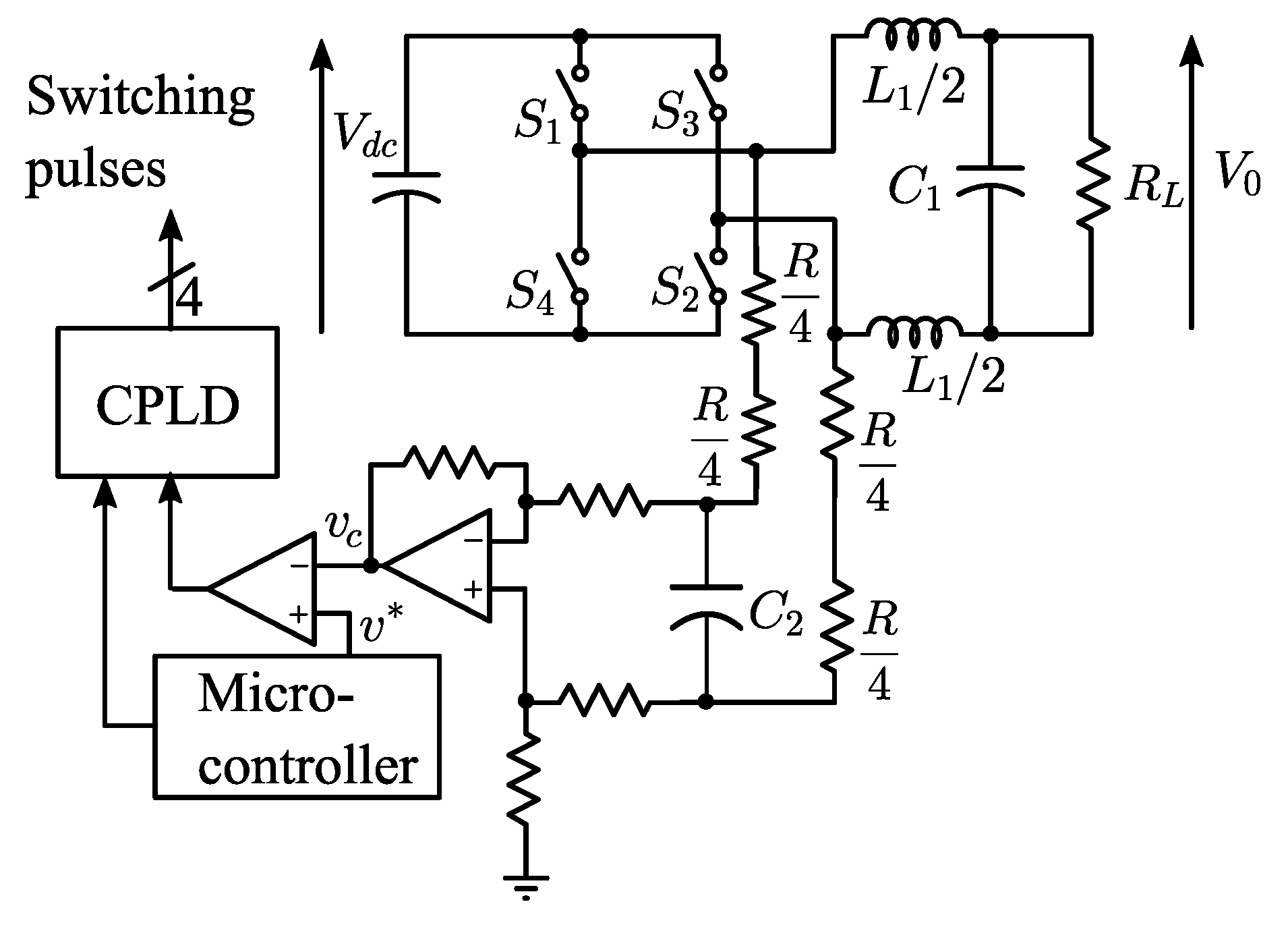
2. System Description

Figure 1 shows the schematic of the voltage source inverter along with the proposed controller. The voltage controller consists of a first-order low-pass filter, differential to single ended converter, comparator, microcontroller, and a CPLD. The sinusoidal reference signal generated by the microcontroller is compared with the low-pass-filtered pole voltages of the inverter to obtain a one-bit logic signal. The CPLD converts this one-bit feedback signal to gate pulses, ensuring a nearly constant switching frequency.
The reference sinusoidal signal generated by the microcontroller is denoted as v * and the feedback signal obtained by filtering the pole voltages is denoted as v c . A detailed algorithm of the proposed control method is presented in Figure 2 and the corresponding switching logic is given in Table 1.
Let ON state be defined as the state wherein switches S 1 , S 2 are ON and S 3 , S 4 are OFF. Similarly, let OFF state be defined as the state wherein switches S 1 , S 2 are OFF and S 3 , S 4 are ON. Let t o n + and t o f f + denote the on-time and off-time during the positive half cycle of the reference wave and t o n and t o f f denote the on-time and off-time during the negative half cycle of the reference wave, respectively.
During the simulation and practical implementation, the maximum switching frequency of the inverter switches is limited to 20 kHz by providing a minimum time duration (T) of 50 μ s between two consecutive turn-off instants in the positive half cycle and two consecutive turn-on instants in the negative half cycle of the reference signal. The equivalent circuit of the system for different switching states is indicated in Figure 3. When switches S 1 , S 2 are ON, the capacitor C 2 charges to a voltage of + V d c through an equivalent resistance R. Similarly, when switches S 3 , S 4 are ON, the capacitor C 2 charges to a voltage of V d c . The expression for the instantaneous voltage across the capacitor v c is given by
v c = v f i n a l + v i n i t i a l v f i n a l e t / R C 2
where v f i n a l and v i n i t i a l are the final value and the initial value of the capacitor voltage, respectively. The approximate slope of the capacitor voltage waveform just after a state change is given by
d v c d t = 1 R C 2 v f i n a l v i n i t i a l e t / R C 2
d v c d t 1 R C 2 v f i n a l v i n i t i a l
The nature of the slope of the capacitor voltage waveform is different during each of the half cycles of the sinusoidal reference signal, and the control algorithm needs to consider the positive and negative half cycles separately. The cases are analysed below.

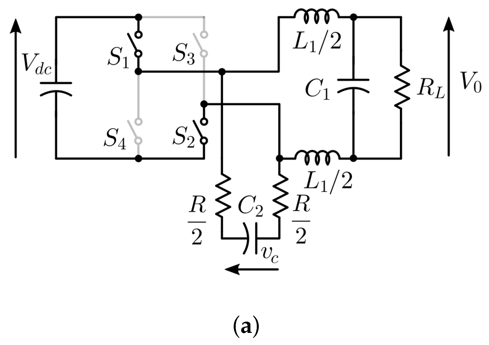
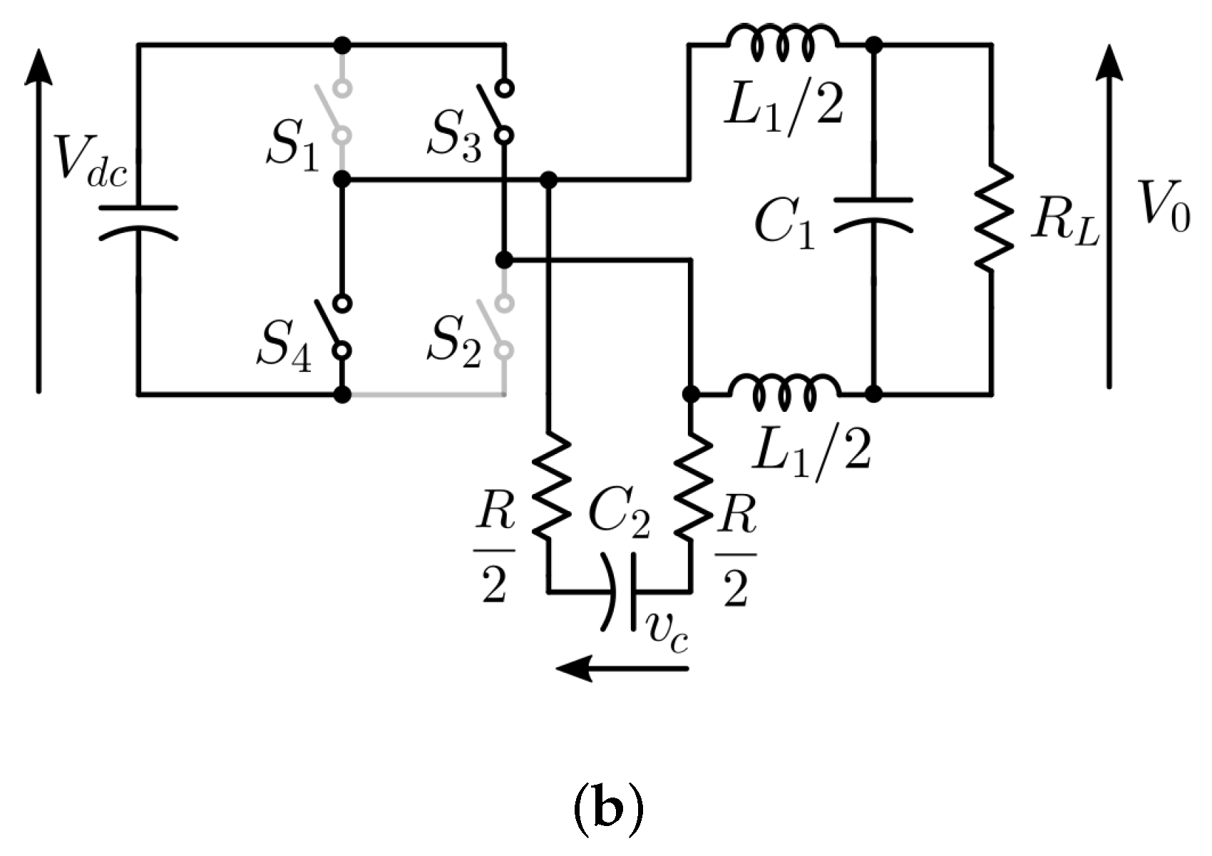
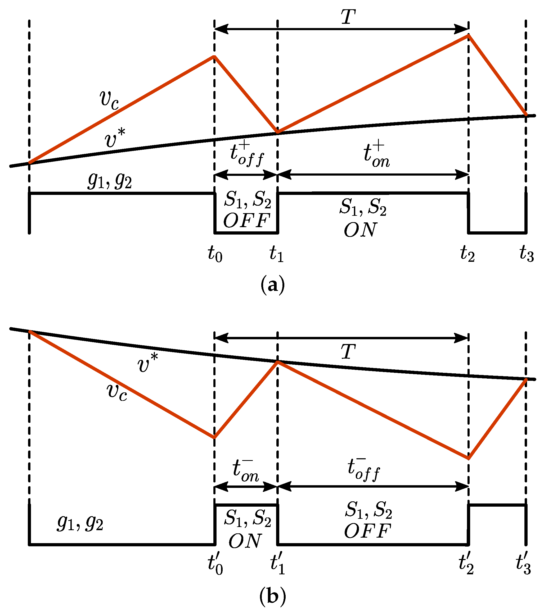
2.1. Case I: Slope of the Capacitor Voltage ( v c ) during Positive Half Cycle of the Reference Signal

In the positive half cycle of the reference signal, the instantaneous value of the capacitor voltage ( v c ) is positive. When switches S 1 , S 2 are ON, from (3), the slope of capacitor voltage is
d v c d t O N = 1 R C 2 V d c v c
In the OFF state, the slope of capacitor voltage is
d v c d t O F F = 1 R C 2 V d c + v c

2.2. Case II: Slope of the Capacitor Voltage during the Negative Half Cycle of the Reference Signal

In the negative half cycle of the reference signal, the instantaneous capacitor voltage ( v c ) is negative. The slope of capacitor voltage, when switches S 1 , S 2 are ON and OFF, are given by (6) and (7), respectively.
d v c d t O N = 1 R C 2 V d c + v c
d v c d t O F F = 1 R C 2 V d c v c

3. Implementation of the Proposed Switching Algorithm

As the rising and falling edges of the capacitor voltage waveform have different slopes, as given in Equations (4)–(7) during each of the half cycles of the reference sine wave, the switching criteria are different for the positive and negative half cycles. A detailed explanation is provided below.

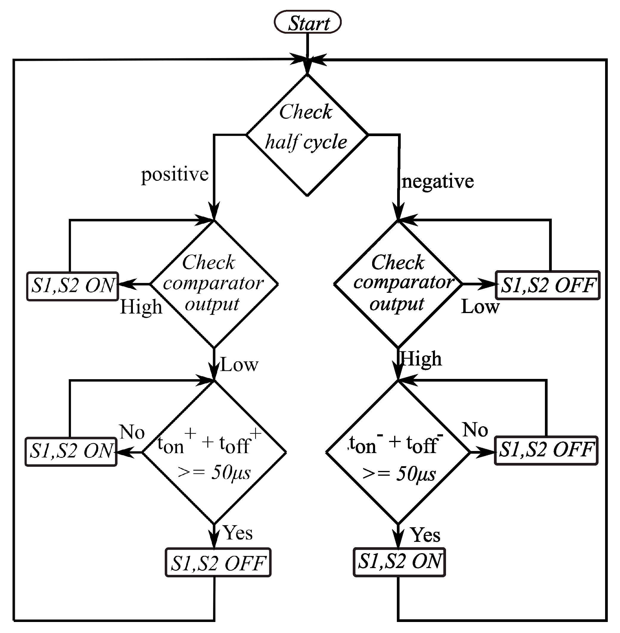
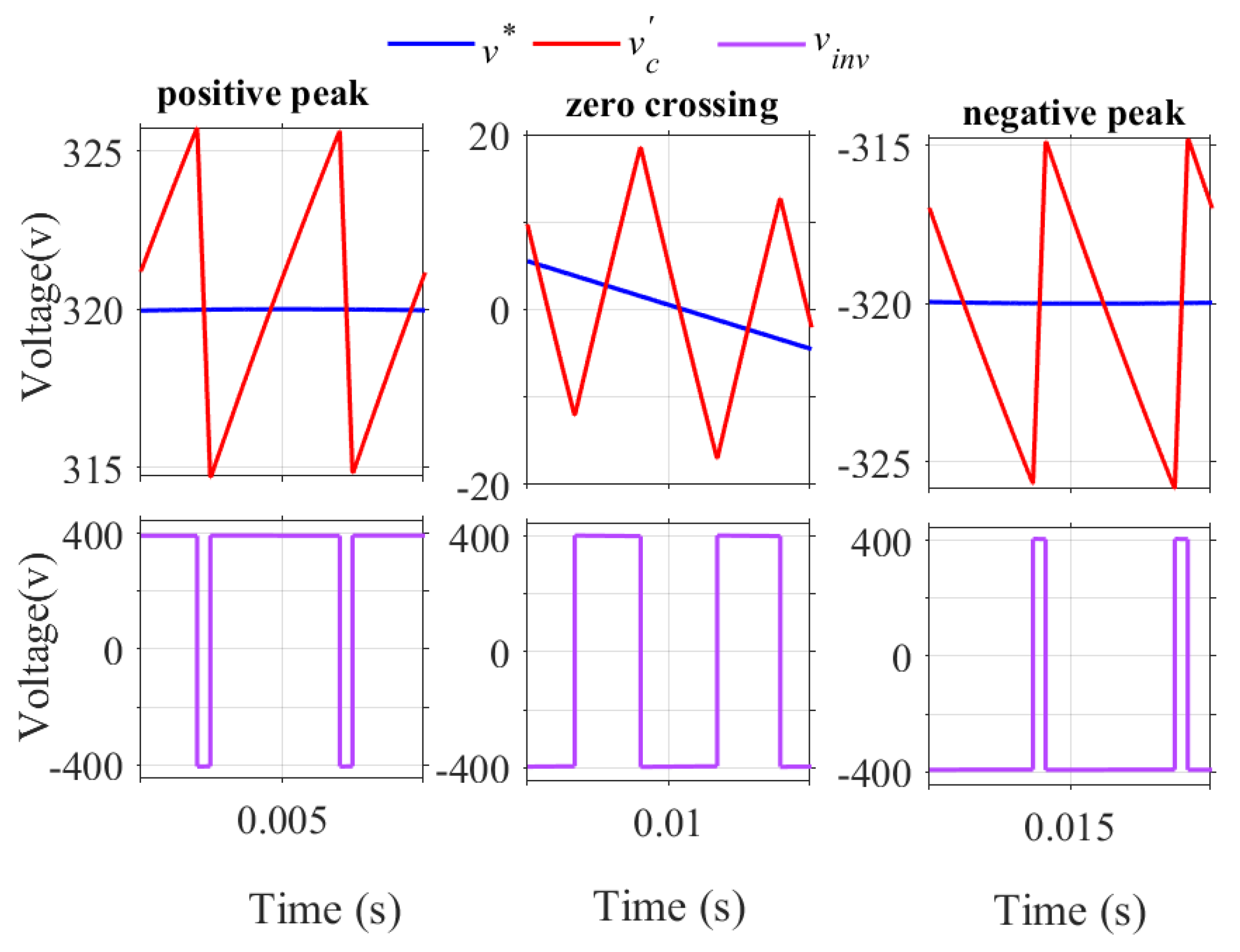
3.1. Switching Criteria during the Positive Half Cycle of Reference Sine Wave

From Equations (4) and (5), it is evident that the falling slope of the capacitor voltage waveform is much larger compared with the rising slope in the case of the positive half cycle. So, the logic selected during the positive half cycle is to control the falling edges of gate pulses g 1 and g 2 using a counter-based approach to ensure a switching period of 50 μ s and the rising edge by the comparator output. By this logic, the minima of the capacitor voltage waveform will always coincide with the reference sine wave during the positive half cycle. Variation of v c , v * and the gate pulses g 1 and g 2 during the positive half cycle is shown in Figure 4a. At the time instant t 0 , switches S 1 and S 2 are turned OFF and the capacitor voltage v c decreases rapidly. A digital counter is also started from 0 at this instant to control the switching period. At the time instant t 1 , v c falls to v * and the comparator output changes from low to high. In response to this change, switches S 1 and S 2 are turned ON by the control logic and the voltage v c rises slowly with a slope given by (4). When the counter reaches a count value corresponding to the switching period of 50 μ s, switches S 1 and S 2 are turned OFF, and this time instant is denoted as t 2 . Now, the capacitor voltage decreases rapidly and continues until the time instant t 3 . At t 3 , v c equals v * , switches S 1 and S 2 are turned ON again, and this process continues. Thus, the switching period is controlled to obtain a constant value of 50 μ s, and the minima of the capacitor voltage waveform will always coincide with the reference sine wave.

3.2. Switching Criteria for the Negative Half Cycle of Reference Sine Wave

During the negative half cycle, the magnitude of the turn-on slope is much higher compared with the turn-off slope, as evident from (6) and (7). Therefore, the capacitor voltage v c rises faster and falls slower in the negative half cycle. Figure 4b shows the variation of v c during the negative half of the reference. The logic selected during the negative half cycle is to control the rising edges of gate pulses g 1 and g 2 using a counter-based approach to ensure a switching period of 50 μ s and the falling edge by the comparator output. Switches S 1 and S 2 are turned OFF when voltage v c rises to reference voltage v * . Thus, the reference voltage v * forms the upper bound for the capacitor voltage v c in the negative half cycle. Switches S 1 and S 2 are then turned ON only when a minimum duration of T seconds has elapsed after the previous turn-on. Thus, the switching period is controlled to obtain a constant value of 50 μ s, and the maxima of the capacitor voltage waveform will always coincide with the reference sine wave.
Figure 5a,b show the variation of v c over one cycle of v * after applying the control logic. A constant switching frequency of 20 kHz can be observed at all angles of the reference sinusoidal wave except for the zero crossings. From the figure, it is observed that the resultant voltage envelope lies above the reference and below the reference during the positive and negative half cycles, respectively. Moreover, the harmonic content of the resultant output waveform does not meet the harmonic requirement as per IEEE standards. In order to address these issues, a modification of the reference signal is proposed in [30,31,32]. It can be achieved by adding an offset to shift the reference waveform downwards during the positive half cycle and upwards during the negative half cycle to obtain the improved waveforms, as shown in Figure 5b. Further improvement of THD and a constant switching frequency at the zero crossings can be achieved by a variable offset approach.

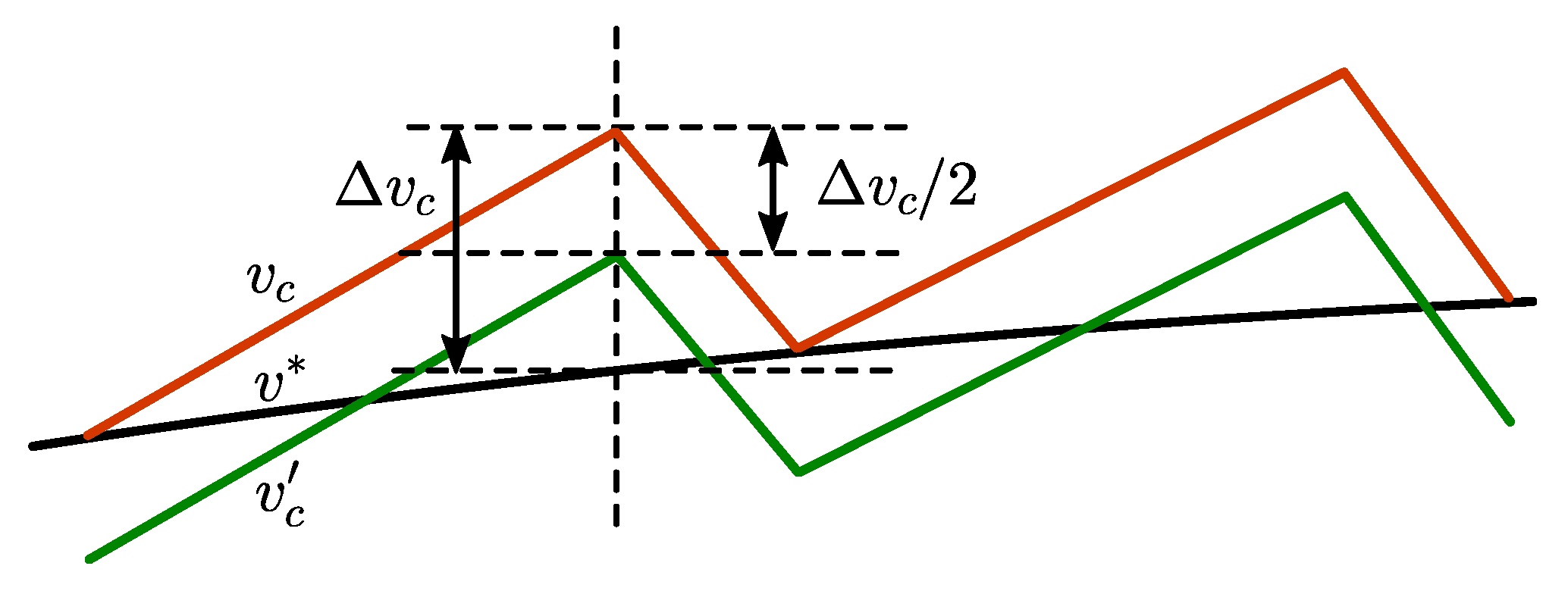
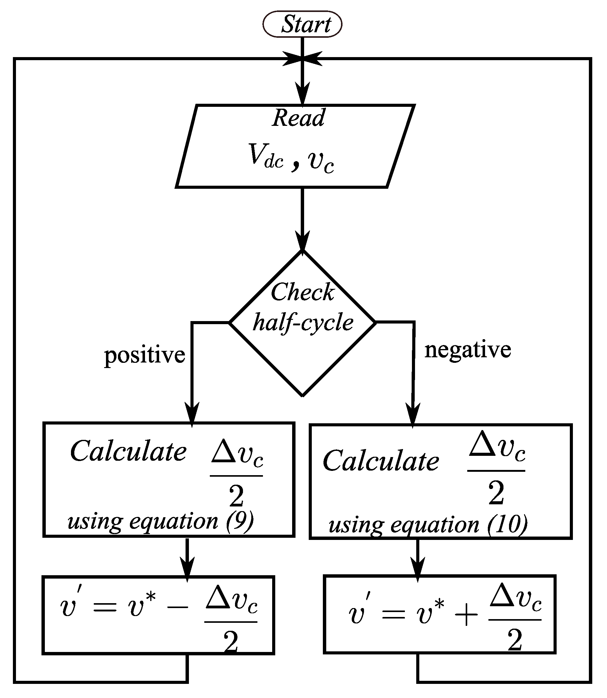
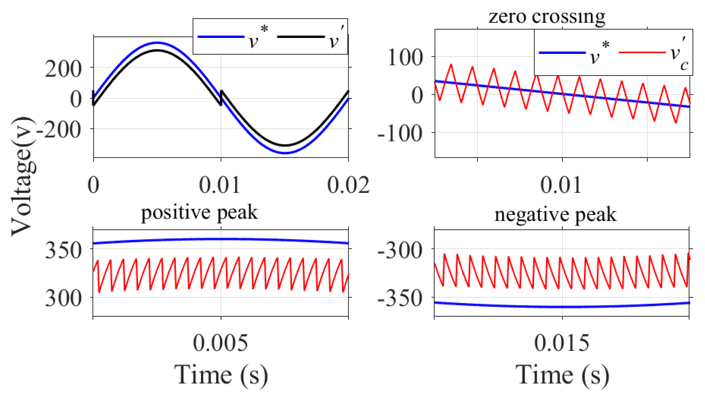
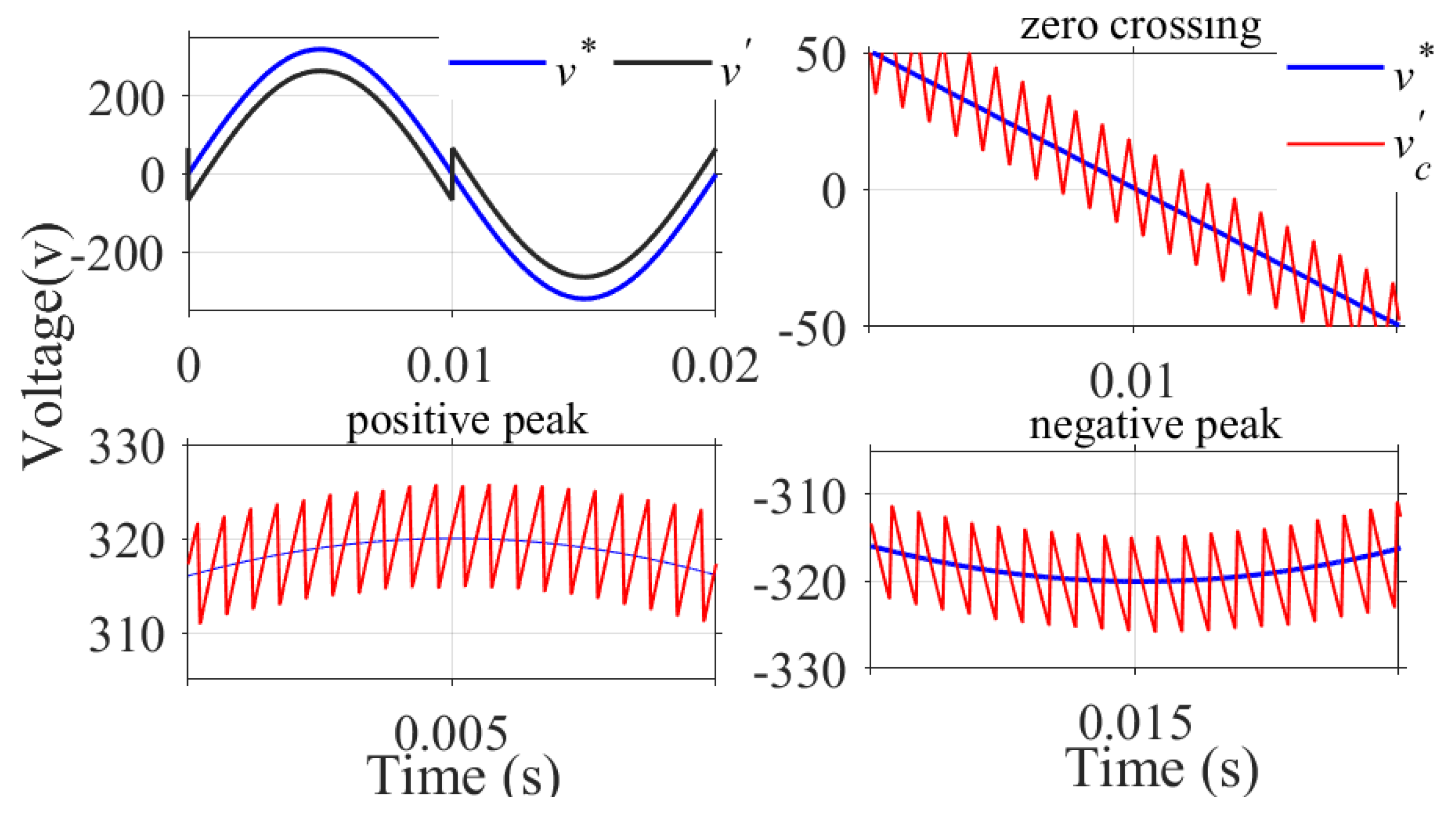
3.3. Computation of Offset Voltage

Figure 6 shows the capacitor voltage denoted by v c , the reference voltage v * , and the modified capacitor voltage denoted by v c . The offset should be added in such a way that the midpoint of the rising and the falling sections of the capacitor voltage waveform is coinciding with the reference sine wave. The peak-to-peak ripple of the capacitor voltage waveform is denoted by Δ v c and the corresponding offset to be added is Δ v c / 2 . The offset needed for the positive half cycle can be calculated by referring to Figure 4a, assuming that the reference sine wave v * is a constant during the switching period. The capacitor voltages at time instants t 1 and t 2 can be written as
v c ( t 1 ) = v c ( t 0 ) + t o f f + . d v c d t O F F
v c ( t 2 ) = v c ( t 1 ) + t o n + . d v c d t O N
The offset to be added to the reference wave during the positive half cycle can be calculated from Equations (4), (5), (8), and (9) and is given by
Δ v c 2 = V d c 2 + v c 2 4 V d c f s R C 2
where f s is the switching frequency. The corresponding offset for the negative half cycle is
Δ v c 2 = V d c 2 v c 2 4 V d c f s R C 2
From (10) and (11), it is evident that the offset depends on the instantaneous value of v c and V d c .

3.4. Modification of the Reference Sine Wave

Offsets specified in Equations (10) and (11) can be used to modify the reference sine wave to obtain a nearly constant switching frequency and good spectral characteristics. Figure 7 shows the flowchart representation of the modification of the reference signal, where v is the modified reference signal. Another simpler method is also discussed in which a fixed offset is used for the entire cycle of the reference sine wave.

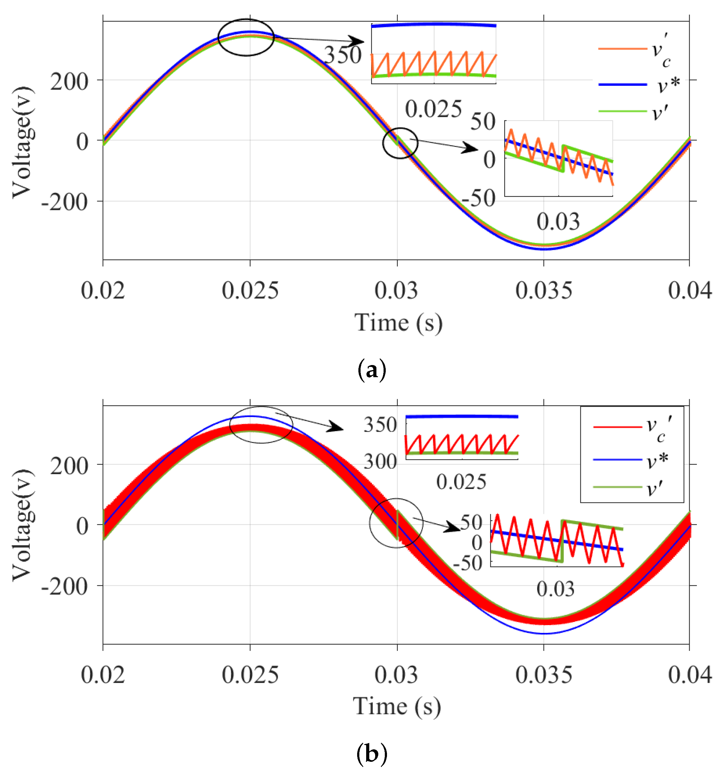
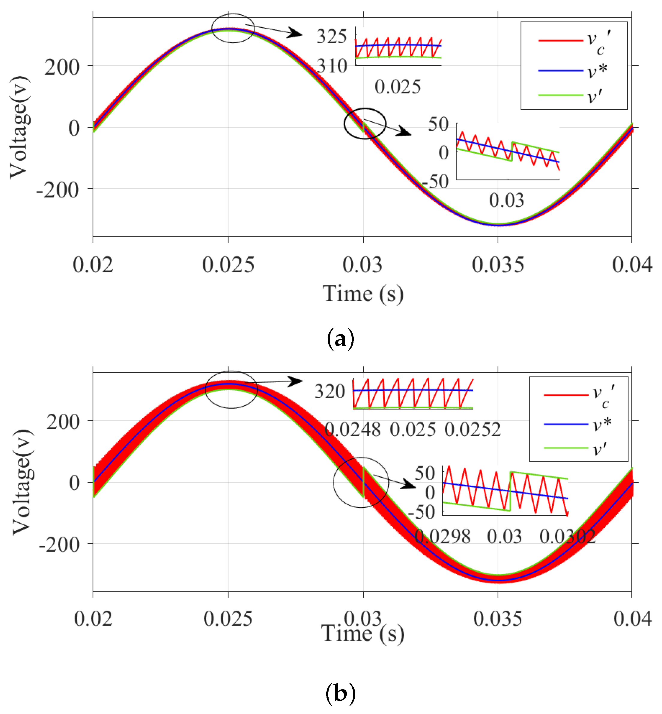
3.4.1. Fixed Offset Correction

The simplest way to modify the reference wave is to add a fixed offset calculated from Equations (10) and (11). The method adopted during the simulation and experiment is to find out the fixed offset value for which the THD content is minimum. During the calculation, the capacitor voltage v c is assumed to be equal to the reference wave. The maximum offset occurs at the zero crossings of the reference, and it is given by
Δ v c 2 m a x = V d c 4 f s R C 2
The minima depend on the modulation index of the reference wave, and they are given by
Δ v c 2 m i n = V d c 1 m 2 4 f s R C 2
where m is the modulation index. The minima occur at odd multiples of π 2 .
Figure 8 illustrates how the output THD is affected by the modification of the reference signal with different fixed offset values. From the illustration, it is clear that the THD improves significantly as the offset varies from its minimum given by (13) to the maximum given by (12). Thus, the maximum offset given by (12) is chosen here as the offset value, which is subtracted from the reference wave during the positive half cycle and added to the reference wave during the negative half cycle to obtain the modified reference wave v . Figure 9 shows the waveforms of the modified reference signal v , reference signal v * , and the feedback voltage v c after providing the {fixed offset given by (12). The zero-crossing distortion observed in Figure 5 is corrected, the switching frequency is maintained constant, and there is a significant improvement in THD. It can also be observed from Figure 9 that the modulation index decreases after providing the offset to the reference signal v * and the resultant modulation index m can be calculated using the expression given by (14).
m = m ( 1 1 4 f s R C 2 m )

3.4.2. Variable Offset Correction

Here, the reference is modified with the offsets specified in Equations (10) and (11), and this calculation is needed for each switching cycle. Figure 10 shows the waveforms of the modified reference signal v , reference signal v * , and the feedback voltage v c after adding the variable offset to the reference signal. The maximum offset is given during zero crossings, and the minimum offset is given during positive and negative peaks of the input signal. The zero-crossing distortion observed in Figure 5 is absent, the maximum switching frequency is maintained constant, and the THD content has improved. Since the offset provided during each switching instant varies according to Equations (10) and (11), the change in modulation index is insignificant here.

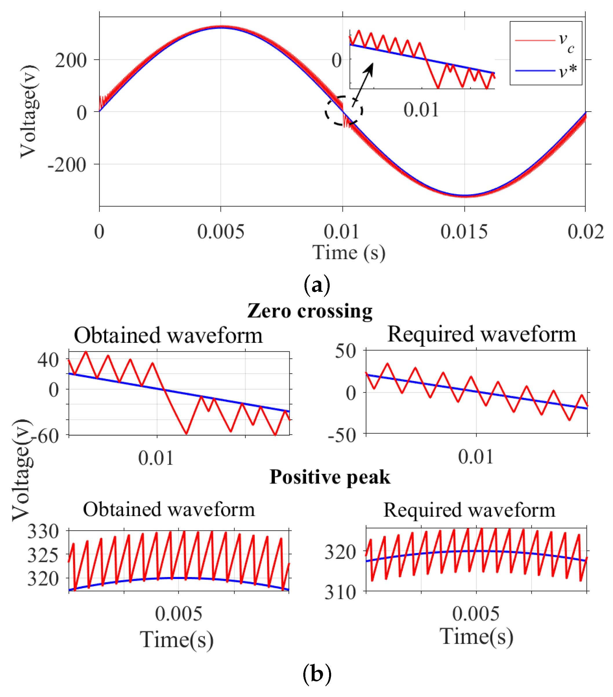
4. Simulation Results

The proposed control method is tested by simulating the system using MATLAB/ SIMULINK R2020a software. A 1 kW, 230 V, 50 Hz VSI feeding a resistive load is considered here. The other simulation parameters are V d c = 400 V and f s = 20 kHz. To attenuate the high-frequency switching components from the output of the inverter, an LC filter for a 1 kHz cut-off frequency is designed. The corresponding values of filter elements are L 1 = 2.5 mH and C 1 = 10 μ F , which provide an attenuation of 52 dB at 20 kHz switching frequency. Under full load conditions, the drop across the filter inductor is obtained as 3.14 V, which is quite small compared with the output voltage and, hence, neglected here. Furthermore, this drop can be compensated by providing additional current feedback and properly controlling the modulation index.
In Figure 1, v c is the first-order-filtered inverter pole voltage, which is being fed to the comparator as the feedback signal. The peak-to-peak ripple of v c is related to the cut-off frequency f c of the feedback path and affects the system performance. The simulations are performed for a range of cut-off frequencies to examine the effect of filtering of the feedback signal on the system. Figure 11 shows the simulation results for the fixed offset correction method where the waveforms of v c , v * , and v are shown for different values of f c .
Figure 12 shows the simulated waveforms of v c , v * , and v using variable offset correction method.
The relationship between the cut-off frequency f c of the feedback path and the output voltage THD using fixed offset correction and variable offset correction is illustrated in Figure 13. At higher values of f c , the ripple content is high, resulting in higher THD at the output. At low values of f c , the peak-to-peak ripple is significantly less such that it is comparable with the noise voltages present in the system, which may cause unwanted switching of the devices in the circuit. In addition, the system response will be slower under dynamic operating conditions for lower values of f c . As a trade-off between the higher and lower values of cut-off frequencies, f c = 0.5 kHz is suitably chosen here. The corresponding THDs observed for fixed offset correction and variable offset correction are 1.25% and 0.76%, respectively. Thus, a THD improvement is obtained using the variable offset correction method.
Figure 14 shows the waveforms of reference signal v * , feedback signal v c , and inverter output pulses v i n v during positive peak, negative peak, and zero crossing using the variable offset correction method, and Figure 15 shows the frequency spectrum of the output voltage. A minimum switching period of 50 μ s is ensured and the computed THD is 0.76%.

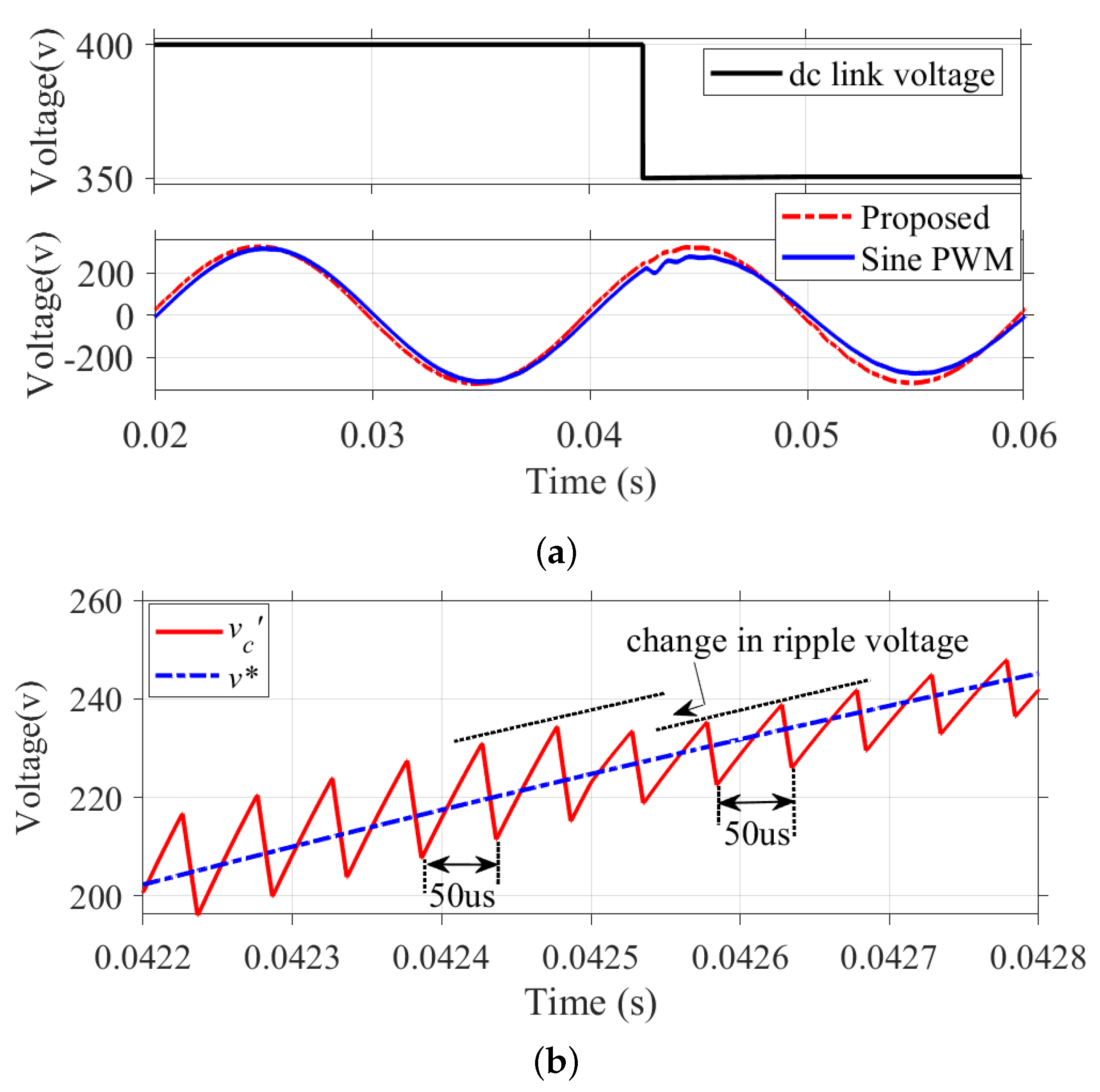
4.1. System Response to Variations in DC Bus Voltage

The system’s dynamic performance with sudden changes in source voltage is simulated here. Figure 16a shows a step reduction in input voltage from 400 to 350 V at t = 0.0425 s. For the proposed method, the output voltage remains regulated, as shown in Figure 16a. The enlarged feedback voltage waveform for this transition is shown in Figure 16b. It is observed that the switching frequency is kept constant before and after the step change. The voltage ripple amplitude after the step change became smaller since the voltage ripple is a function of input dc voltage, as shown in (10) and (11).
Figure 16a also shows the response of the system for the same reduction in input voltage by employing the conventional Sine PWM control technique. It can be seen that the magnitude of output voltage reduces by about 40 V in the case of Sine PWM, whereas the reduction in output voltage for the proposed method is only about 3 V.

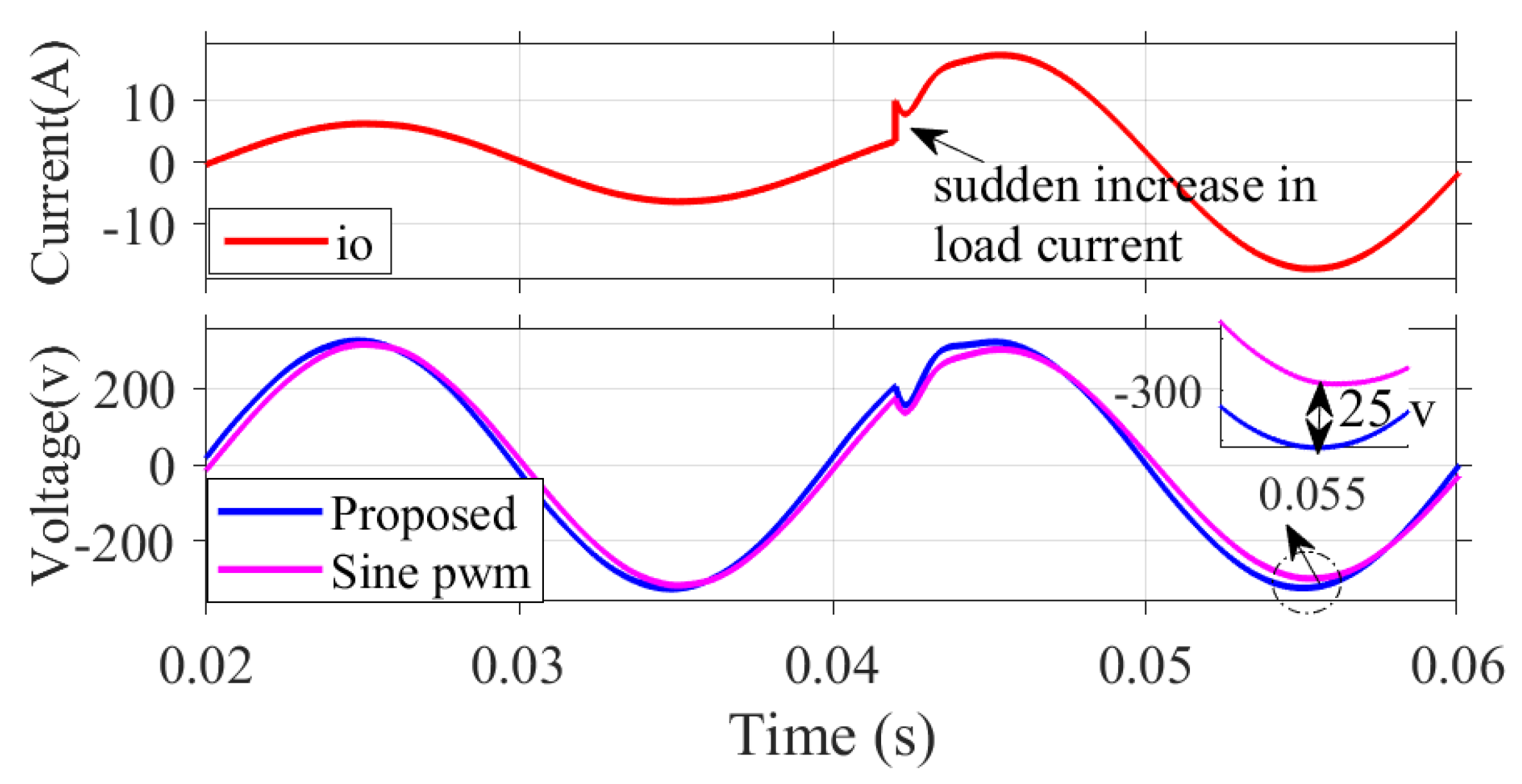
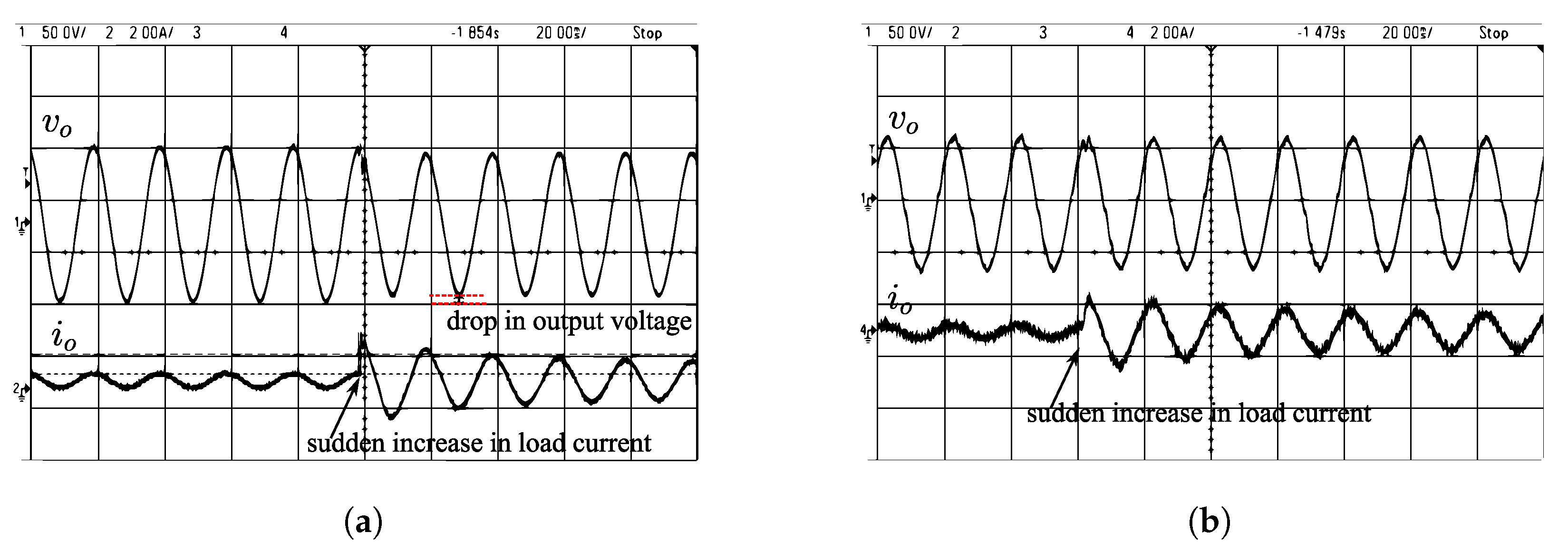
4.2. System Response to Load Variations

The response of the proposed system to sudden changes in load current is discussed here. For the experiment, the internal resistance of MOSFET switches R d s is taken as 0.05 Ω , and the source resistance is taken as 1 Ω . In Figure 17, at t = 0.042 s, the load current increases suddenly to about three times the initial value. It may be observed that the output voltage dips initially but restores suddenly within 1 ms. The proposed method effectively compensates for the voltage drop across the switches and source impedance during transient operating conditions, thereby regulating the output voltage across the load.
A comparison of the proposed method against the conventional Sine PWM in terms of response to load changes is also presented here. For the same increase in load current, the output voltage drops by about 25 V for the Sine PWM-based control. Thus, the Sine PWM method needs an extra PID controller for regulating the output voltage at the reference value [33], whereas, in the proposed method, the output voltage regulation is provided by the switching algorithm itself without any additional requirement of controllers. Further, the stability problems associated with PID controllers should be separately addressed [34], whereas the proposed hysteresis-based control method is free from such stability problems.
The system performance under nonlinear load conditions is also experimented. Figure 18a shows the simulated waveforms of load voltage and current while feeding a nonlinear load and Figure 18b shows the corresponding output voltage harmonic spectrum.

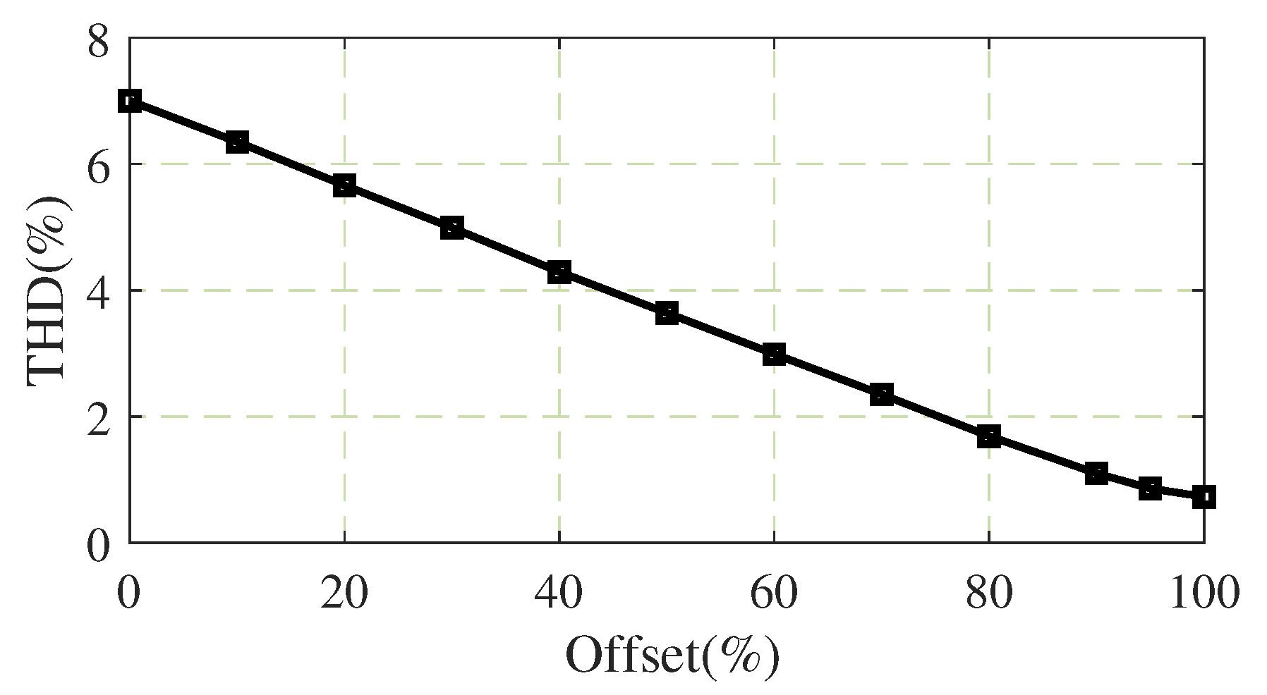
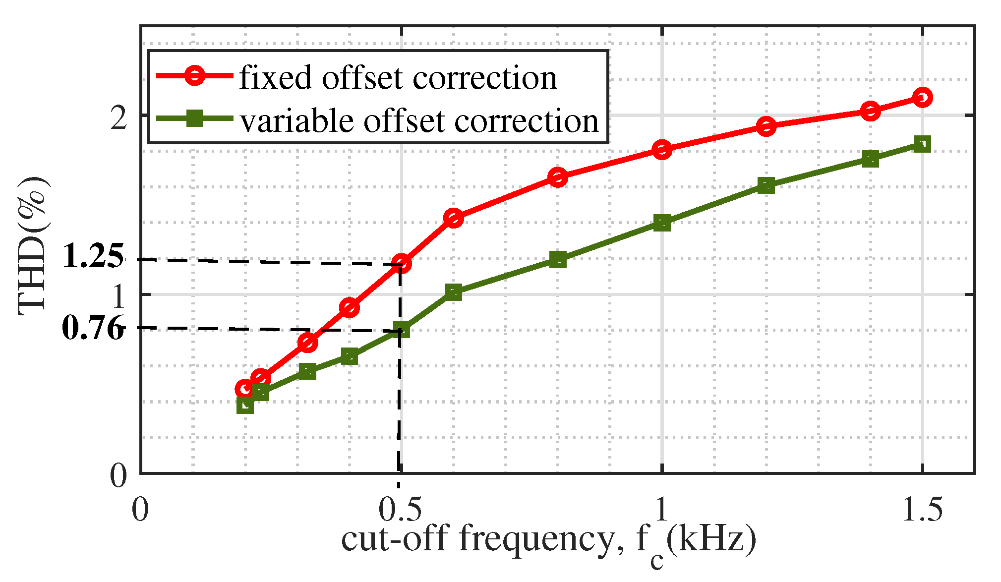
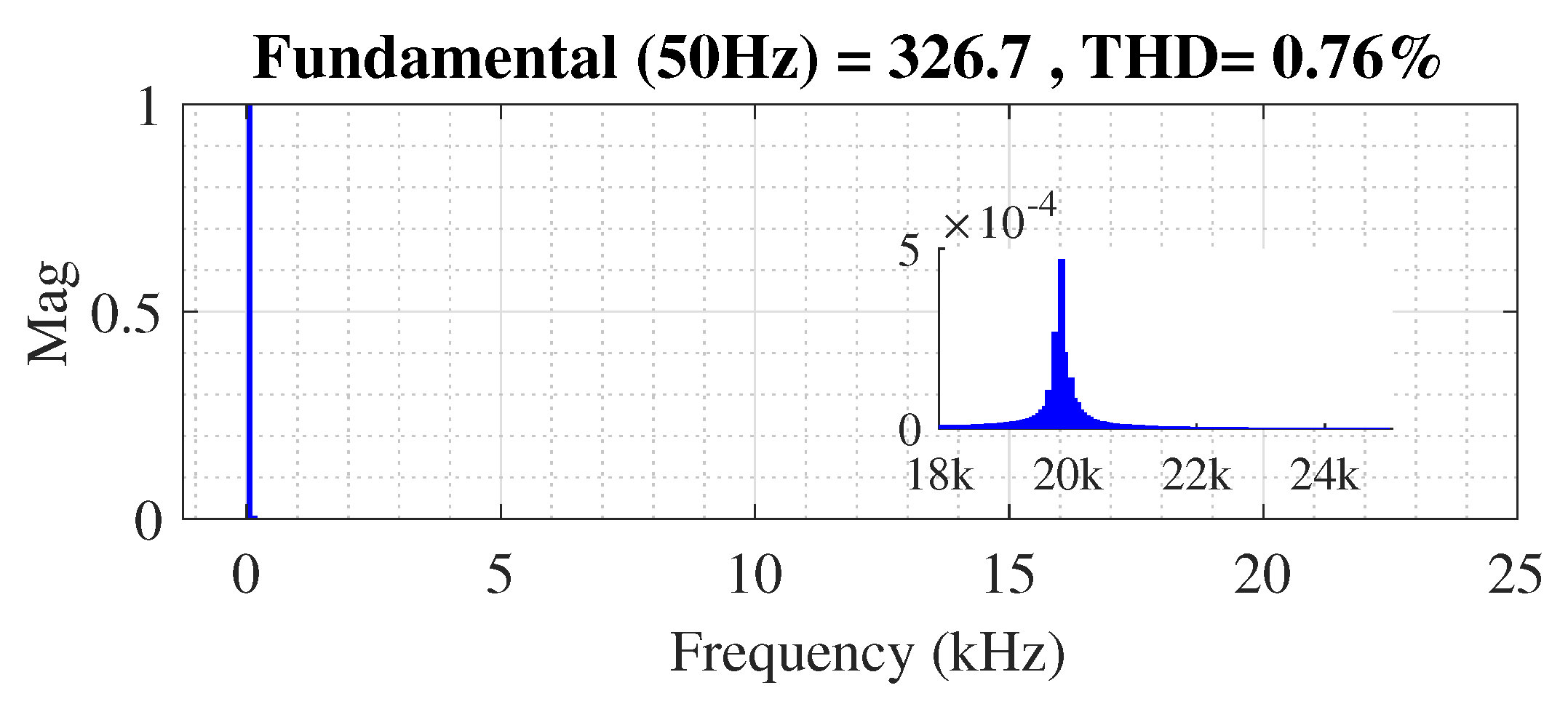
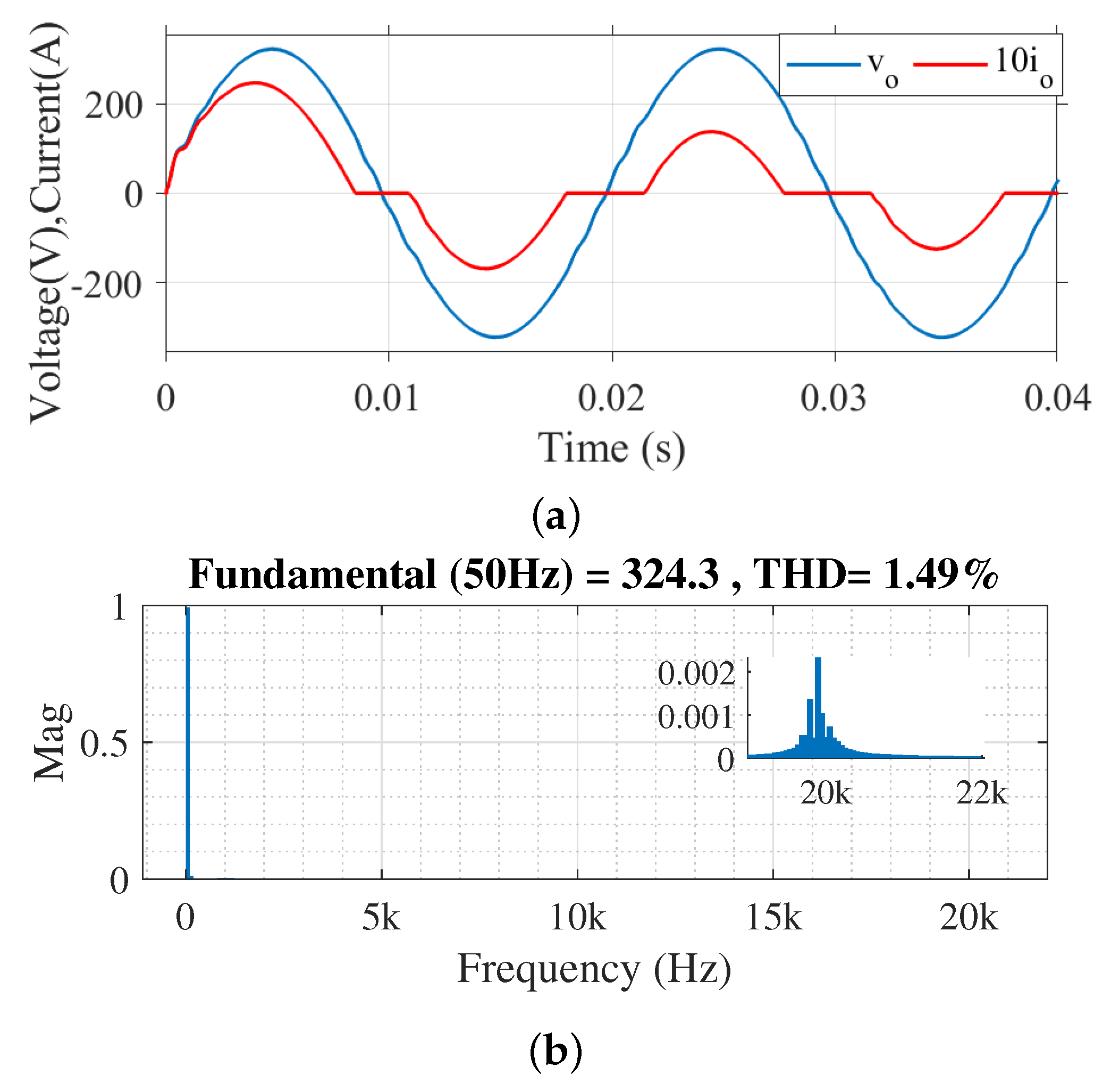
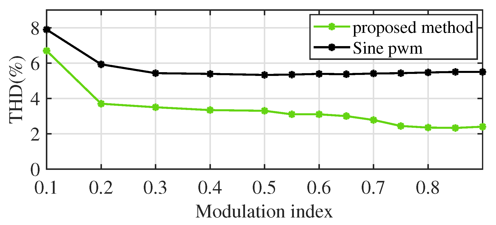
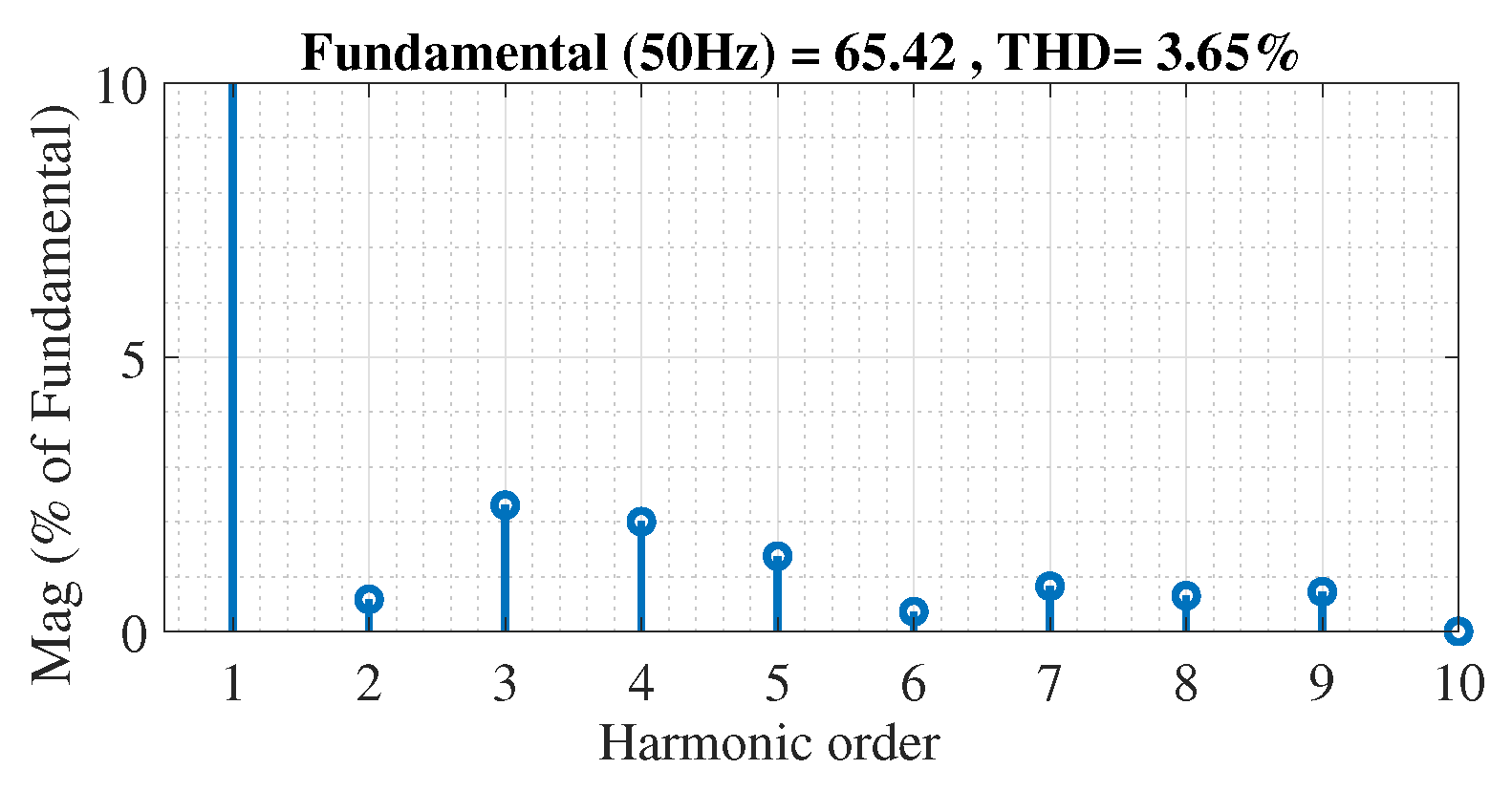
4.3. THD Comparison with Conventional Sine PWM

A comparison in terms of THD is made for a special case in which the rectified voltage of a three-phase diode bridge rectifier is taken as the dc-link voltage. Figure 19 illustrates the THD variation for different modulation indices by employing the proposed control and Sine PWM techniques. It may be noted that the THD obtained for the proposed method is comparatively low; the average reduction in THD is around 2%.

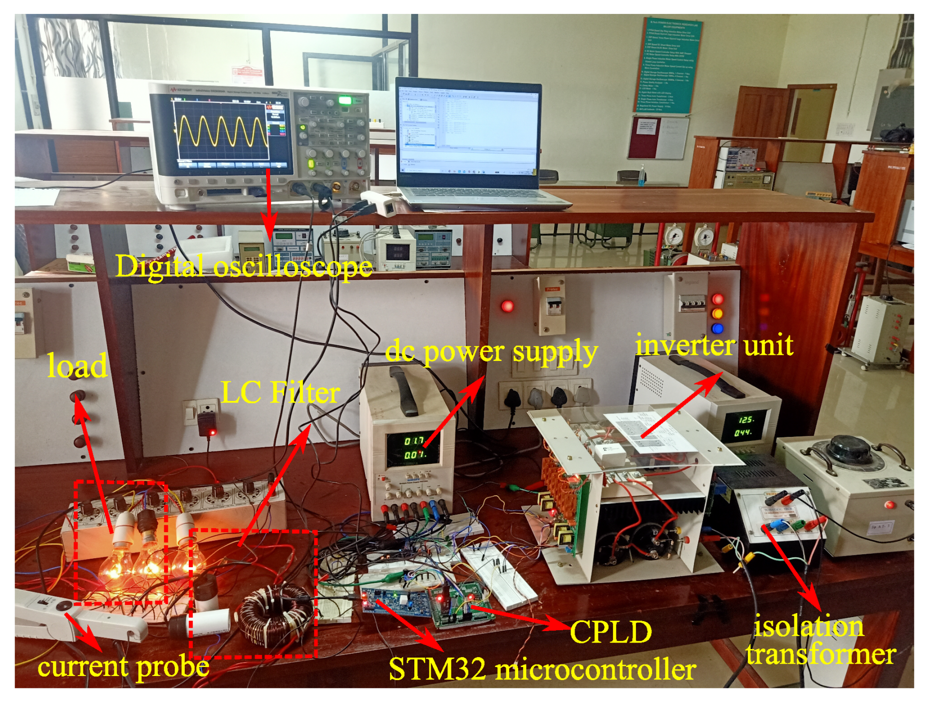
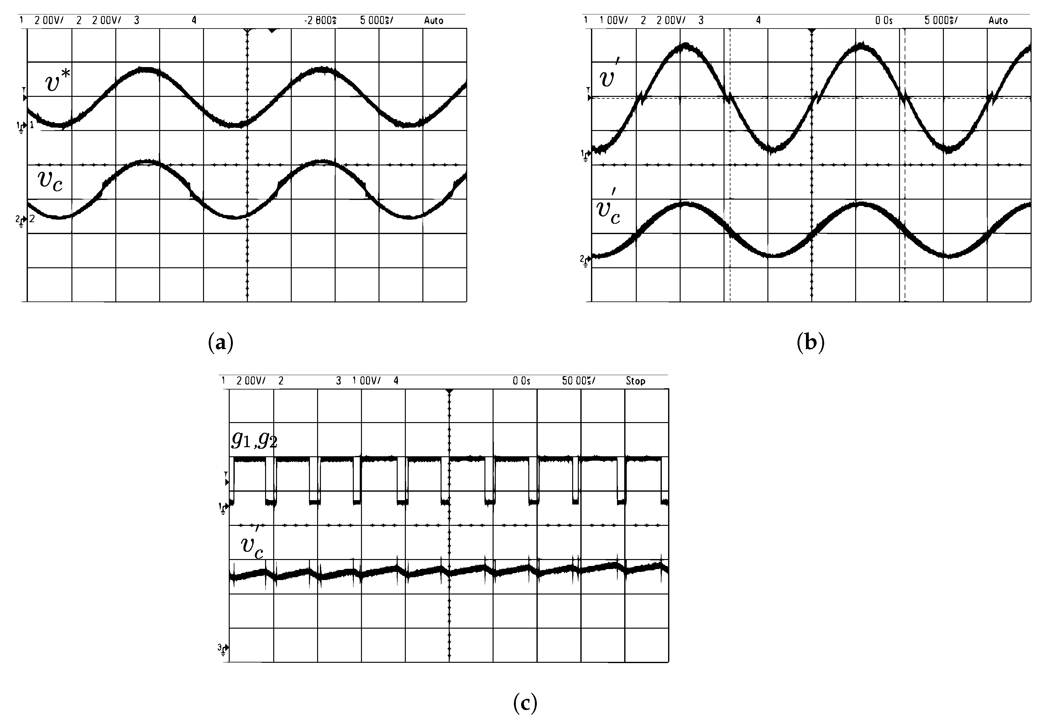
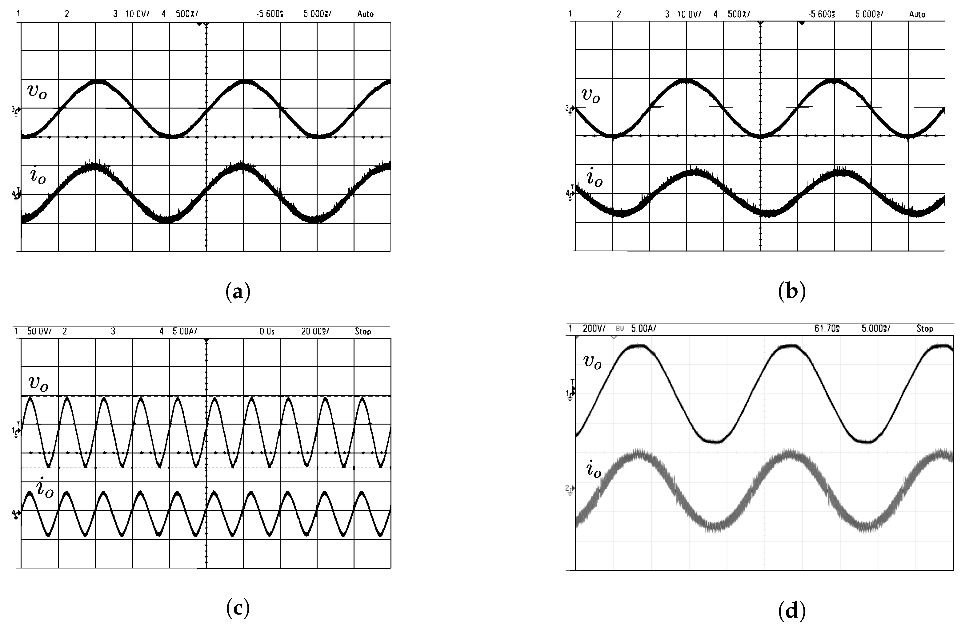
5. Hardware Implementation

The proposed control technique is tested on a single-phase full-bridge inverter, and the hardware set-up is shown in Figure 20. The prototype’s parameters are input dc voltage = 400 V, switching frequency f s = 20 kHz, output fundamental frequency f o = 50 Hz, L 1 = 2.5 mH, C 1 = 10 μ F, C 2 = 0.01 μ F, and R = 4 M Ω .
The inverter circuit comprises four IGBT(SKM100GB12T4) switches driven by isolated gate drivers. The control algorithm specified in Table 1 is implemented using XC9536 CPLD. The 32-bit STM32F334C8 microcontroller is used to generate the modified sine reference. As shown in Figure 1, the CPLD generates gate pulses for the inverter switches ensuring a nearly constant switching frequency. Figure 21a shows the variation of v c , when v * is given as the reference signal to the comparator. The zero crossing distortion of v c can be clearly seen, which is corrected in Figure 21b, where the modified reference v is given as reference signal to the comparator. The corresponding switching signals are shown in Figure 21c.
The load voltage and current waveforms obtained during the experiment for different load conditions are given in Figure 22.
The output voltage harmonic spectrum is shown in Figure 23 and the THD obtained is 3.65%.
The experimental results for a sudden increase in load current due to the addition of an extra load (100 W lamp load) in the system is shown in Figure 24. For the Sine PWM method, the sudden rise in load current creates a drop in output voltage by around 9 V. In contrast, the same increase in load current causes a voltage reduction of below 2 V in the proposed method.
Figure 25 shows the system’s dynamic response when subjected to a sudden reduction in dc link voltage of around 20%. The output voltage drops by about 12.5 V for the Sine PWM method, whereas the output voltage remains regulated irrespective of this change for the proposed control method, as can be seen in Figure 25b.

6. Conclusions

This paper proposes a hysteresis-based control method for the voltage control of single-phase voltage source inverters that does not employ pulse width modulation. The switching signals are generated by a CPLD-based control algorithm that maintains the essential characteristics of the hysteresis control technique while ensuring a nearly constant switching frequency. Using the low-pass-filtered inverter output voltage as the feedback signal ensures a quick dynamic response comparable to the hysteresis control method. The proposed method also provides a well-defined harmonic spectrum comparable to the conventional Sine PWM method during steady-state operation and a better harmonic spectrum when the dc link voltage fluctuates significantly. The system’s steady-state and dynamic conditions are experimentally validated and the results are presented. A comparison between the proposed technique and conventional Sine PWM is also performed to determine its efficacy. The simulation and experimental results demonstrate that the proposed control method is capable of regulating the output voltage during load and source side variations. As a future scope, the proposed method can be applied to three-phase systems feeding industrial and motor loads.

Author Contributions

Conceptualization, G.C. and M.K.; methodology, G.C. and M.K.; software, G.C.; validation, G.C., L.S. and M.K.; formal analysis, G.C., L.S. and M.K.; investigation, B.M.J. and M.K.; resources, G.C. and B.M.J.; writing—original draft preparation, G.C. and N.J.; writing—review and editing, G.C., N.J. and M.K.; visualization, G.C., L.S. and M.K.; supervision, M.K. and B.M.J.; project administration, G.C. All authors have read and agreed to the published version of the manuscript.

Funding

This research received no external funding.

Data Availability Statement

Not applicable.

Conflicts of Interest

The authors declare no conflict of interest.

References

  1. Vithayathil, J. Power Electronics Principles and Applications; McGraw Hill Education: New York, NY, USA, 2010. [Google Scholar]
  2. Moustafa, M.M.Z.; Aboushal, M.A.; EL-Fouly, T.H.; Al-Durra, A.; Zeineldin, H. A novel unified controller for grid-connected and islanded operation of PV-fed single-stage inverter. IEEE Trans. Sustain. Energy 2021, 12, 1960–1973. [Google Scholar] [CrossRef]
  3. Xue, Y.; Chang, L.; Kjaer, S.B.; Bordonau, J.; Shimizu, T. Topologies of single-phase inverters for small distributed power generators: An overview. IEEE Trans. Power Electron. 2004, 19, 1305–1314. [Google Scholar] [CrossRef]
  4. Habibullah, A.F.; Yoon, S.-J.; Tran, T.V.; Kim, Y.; Tran, D.T.; Kim, K.-H. The Recent Development of Power Electronics and AC Machine Drive Systems. Energies 2022, 15, 7913. [Google Scholar] [CrossRef]
  5. Gonzales-Zurita, Ó.; Clairand, J.M.; Peñalvo-López, E.; Escrivá-Escrivá, G. Review on multi-objective control strategies for distributed generation on inverter-based microgrids. Energies 2020, 13, 3483. [Google Scholar] [CrossRef]
  6. Hava, A.; Kerkman, R.; Lipo, T. Carrier-based PWM-VSI overmodulation strategies: Analysis, comparison, and design. IEEE Trans. Power Electron. 1998, 13, 674–689. [Google Scholar] [CrossRef] [Green Version]
  7. Holtz, J.; Lotzkat, W.; Khambadkone, A.M. On continuous control of PWM inverters in the overmodulation range including the six-step mode. IEEE Trans. Power Electron. 1993, 8, 546–553. [Google Scholar] [CrossRef]
  8. Jacobina, C.; Nogueira Lima, A.; da Silva, E.; Alves, R.; Seixas, P. Digital scalar pulse-width modulation: A simple approach to introduce nonsinusoidal modulating waveforms. IEEE Trans. Power Electron. 2001, 16, 351–359. [Google Scholar] [CrossRef]
  9. Bolognani, S.; Zigliotto, M. Novel digital continuous control of SVM inverters in the overmodulation range. IEEE Trans. Ind. Appl. 1997, 33, 525–530. [Google Scholar] [CrossRef]
  10. Van Der Broeck, H.W.; Skudelny, H.C.; Stanke, G.V. Analysis and realization of a pulsewidth modulator based on voltage space vectors. IEEE Trans. Ind. Appl. 1988, 24, 142–150. [Google Scholar] [CrossRef]
  11. Zhou, K.; Wang, D. Relationship between space-vector modulation and three-phase carrier-based PWM: A comprehensive analysis [three-phase inverters]. IEEE Trans. Ind. Electron. 2002, 49, 186–196. [Google Scholar] [CrossRef]
  12. Rahman, M.A.; Quaicoe, J.E.; Choudhury, M.A. Performance Analysis of Delta Modulated PWM Inverters. IEEE Trans. Power Electron. 1987, 3, 227–233. [Google Scholar] [CrossRef]
  13. Abdel-Rahim, N.; Quaicoe, J. A single-phase delta-modulated inverter for UPS applications. IEEE Trans. Ind. Electron. 1993, 40, 347–354. [Google Scholar] [CrossRef]
  14. Bowes, S.; Holliday, D.; Grewal, S. Comparison of single-phase three-level pulse width modulation strategies. IEE Proc.-Electr. Power Appl. 2004, 151, 205–214. [Google Scholar] [CrossRef]
  15. Rahman, K.; Khan, M.; Choudhury, M.; Rahman, M. Variable-band hysteresis current controllers for PWM voltage-source inverters. IEEE Trans. Power Electron. 1997, 12, 964–970. [Google Scholar] [CrossRef]
  16. Bose, B. An adaptive hysteresis-band current control technique of a voltage-fed PWM inverter for machine drive system. IEEE Trans. Ind. Electron. 1990, 37, 402–408. [Google Scholar] [CrossRef]
  17. Yao, Q.; Holmes, D. A simple, novel method for variable-hysteresis-band current control of a three phase inverter with constant switching frequency. In Proceedings of the Conference Record of the 1993 IEEE Industry Applications Conference Twenty-Eighth IAS Annual Meeting, Toronto, ON, Canada, 2–8 October 1993; Volume 2, pp. 1122–1129. [Google Scholar] [CrossRef]
  18. Rashidi, N. Improved and less load dependent three-phase current-controlled inverter with hysteretic current controllers. IEEE Trans. Ind. Electron. 1995, 42, 325–330. [Google Scholar] [CrossRef]
  19. Tripathi, A.; Sen, P. Comparative analysis of fixed and sinusoidal band hysteresis current controllers for voltage source inverters. IEEE Trans. Ind. Electron. 1992, 39, 63–73. [Google Scholar] [CrossRef]
  20. Wu, F.; Feng, F.; Luo, L.; Duan, J.; Sun, L. Sampling period online adjusting-based hysteresis current control without band with constant switching frequency. IEEE Trans. Ind. Electron. 2015, 62, 270–277. [Google Scholar] [CrossRef]
  21. Wu, F.; Zhang, L.; Wu, Q. Simple unipolar maximum switching frequency limited hysteresis current control for grid-connected inverter. IET Power Electron. 2014, 7, 933–945. [Google Scholar] [CrossRef]
  22. Ho, C.N.; Cheung, V.S.; Chung, H.S. Constant-frequency hysteresis current control of grid-connected VSI without bandwidth control. In Proceedings of the 2009 IEEE Energy Conversion Congress and Exposition, San Jose, CA, USA, 20–24 September 2009; pp. 2949–2956. [Google Scholar] [CrossRef]
  23. Rata, G.; Marschalko, R. Development of Hysteresis Modulation Methods for PWM AC-to-DC Converters Based on Dead-Beat Control. In Proceedings of the 2006 IEEE International Conference on Automation, Quality and Testing, Robotics, Cluj-Napoca, Romania, 25–28 May 2006; Volume 1, pp. 220–224. [Google Scholar] [CrossRef]
  24. Stefanutti, W.; Mattavelli, P. Fully digital hysteresis modulation with switching-time prediction. IEEE Trans. Ind. Appl. 2006, 42, 763–769. [Google Scholar] [CrossRef]
  25. Komurcugil, H.; Ozdemir, S.; Sefa, I.; Altin, N.; Kukrer, O. Sliding-Mode Control for Single-Phase Grid-Connected LCL-Filtered VSI With Double-Band Hysteresis Scheme. IEEE Trans. Ind. Electron. 2016, 63, 864–873. [Google Scholar] [CrossRef]
  26. Abrishamifar, A.; Ahmad, A.; Mohamadian, M. Fixed Switching Frequency Sliding Mode Control for Single-Phase Unipolar Inverters. IEEE Trans. Power Electron. 2012, 27, 2507–2514. [Google Scholar] [CrossRef]
  27. Kumar, N.; Saha, T.K.; Dey, J. Sliding-Mode Control of PWM Dual Inverter-Based Grid-Connected PV System: Modeling and Performance Analysis. IEEE J. Emerg. Sel. Top. Power Electron. 2016, 4, 435–444. [Google Scholar] [CrossRef]
  28. Makhamreh, H.; Trabelsi, M.; Kükrer, O.; Abu-Rub, H. An effective sliding mode control design for a grid-connected PUC7 multilevel inverter. IEEE Trans. Ind. Electron. 2019, 67, 3717–3725. [Google Scholar] [CrossRef]
  29. Repecho, V.; Biel, D.; Olm, J.M. A Simple Switching-Frequency-Regulated Sliding-Mode Controller for a VSI with a Full Digital Implementation. IEEE J. Emerg. Sel. Top. Power Electron. 2020, 9, 569–579. [Google Scholar] [CrossRef]
  30. Lyu, J.; Hu, W.; Wu, F.; Yao, K.; Wu, J. Variable modulation offset SPWM control to balance the neutral-point voltage for three-level inverters. IEEE Trans. Power Electron. 2015, 30, 7181–7192. [Google Scholar] [CrossRef]
  31. Odeh, C.; Kondratenko, D.; Lewicki, A.; Jąderko, A. Modified SPWM Technique with Zero-Sequence Voltage Injection for a Five-Phase, Three-Level NPC Inverter. Energies 2021, 14, 1198. [Google Scholar] [CrossRef]
  32. Giri, S.K.; Chakrabarti, S.; Banerjee, S.; Chakraborty, C. A carrier-based PWM scheme for neutral point voltage balancing in three-level inverter extending to full power factor range. IEEE Trans. Ind. Electron. 2016, 64, 1873–1883. [Google Scholar] [CrossRef]
  33. Zeng, D.; Zheng, Y.; Luo, W.; Hu, Y.; Cui, Q.; Li, Q.; Peng, C. Research on improved auto-tuning of a pid controller based on phase angle margin. Energies 2019, 12, 1704. [Google Scholar] [CrossRef] [Green Version]
  34. Marati, N.; Prasad, D. A modified feedback scheme suitable for repetitive control of inverter with nonlinear load. IEEE Trans. Power Electron. 2017, 33, 2588–2600. [Google Scholar] [CrossRef]
Figure 1. Schematic of voltage mode controller based single-phase full bridge voltage source inverter.
Energies 16 00783 g001
Figure 2. Control algorithm of the proposed method.
Energies 16 00783 g002
Figure 3. Equivalent circuit of the system when (a) S 1 , S 2 : ON and (b) S 1 , S 2 : OFF.
Energies 16 00783 g003aEnergies 16 00783 g003b
Figure 4. Sketch of voltage waveform within two switching cycles during (a) positive half cycle and (b) negative half cycle.
Energies 16 00783 g004
Figure 5. (a) Variation of v c , v * over one cycle of reference signal. (b) Variation of v c along with their ideally required waveshape near zero crossings and near the positive peak.
Energies 16 00783 g005
Figure 6. Deviation in output voltage.
Energies 16 00783 g006
Figure 7. Modification of the reference signal.
Energies 16 00783 g007
Figure 8. THD vs. Fixed offset.
Energies 16 00783 g008
Figure 9. Waveforms of v c , v * , and v with fixed offset correction.
Energies 16 00783 g009
Figure 10. Waveforms of v c , v * , and v with variable offset correction.
Energies 16 00783 g010
Figure 11. Fixed offset correction: Simulated waveforms of v c , v * , and v for different cut-off frequencies. (a) f c = 0.5 kHz; (b) f c = 1.5 kHz.
Energies 16 00783 g011
Figure 12. Variable offset correction: Simulated waveforms of v c , v * , and v for different cut-off frequencies. (a) f c = 0.5 kHz; (b) f c = 1.5 kHz.
Energies 16 00783 g012
Figure 13. Relationship between THD and f c using the fixed and variable offset correction methods.
Energies 16 00783 g013
Figure 14. Inverter output pulses for variable offset correction during positive peak, zero crossing, and negative peak.
Energies 16 00783 g014
Figure 15. Output voltage THD.
Energies 16 00783 g015
Figure 16. Variation of output voltage for a step reduction in V d c : (a) Simulated waveform of output voltage for varying dc bus voltage. (b) Output voltage waveform enlarged around step change.
Energies 16 00783 g016
Figure 17. Variation of output voltage waveform for a sudden change in load current at t = 0.042 s.
Energies 16 00783 g017
Figure 18. Simulation results of the system while feeding a nonlinear load. (a) Output voltage and current waveforms. (b) Harmonic spectrum of output voltage.
Energies 16 00783 g018
Figure 19. Voltage THD (%) for the proposed method and Sine PWM method for different modulation indices, where dc link voltage is the rectified output of a three-phase diode bridge rectifier circuit.
Energies 16 00783 g019
Figure 20. Hardware set up.
Energies 16 00783 g020
Figure 21. Experimental results under steady state (a) top trace: v * (2 V/div), bottom trace: v c (2 V/div); (b) top trace: v (1 V/div), bottom trace: v c (2 V/div); (c) top trace: g 1 , g 2 (2 V/div), bottom trace: v c (1 V/div).
Energies 16 00783 g021
Figure 22. Experimental results under steady state (a) top trace: load voltage v o (10 V/div), bottom trace: load current i o (500 mA/div) for R load = 10 Ω , 10 W; (b) top trace: load voltage v o (10 V/div), bottom trace: load current i o (500 mA/div) for R-L load, R = 10 Ω , 10 W, L = 12 mH; (c) top trace: load voltage v o (50 V/div), bottom trace: load current i o (5 A/div) for 100 W lamp load; (d) top trace: load voltage v o (200 V/div), bottom trace: load current i o (5 A/div) for 1000 W load.
Energies 16 00783 g022
Figure 23. Harmonic spectrum of output voltage.
Energies 16 00783 g023
Figure 24. Performance comparison of the proposed system with conventional Sine PWM during transient operating conditions. (a) Sine PWM: sudden addition of extra 100 W load, top trace: v o (50 V/div), bottom trace: i o (2 A/div). (b) Proposed logic: sudden addition of extra 100 W load, top trace: v o (50 V/div), bottom trace: i o (2 A/div).
Energies 16 00783 g024
Figure 25. Performance comparison of the proposed system with conventional Sine PWM during a reduction in dc-link voltage of 20%. (a) Sine PWM: top trace: v o (50 V/div), bottom trace: i o (2 A/div). (b) Proposed logic: top trace: v o (50 V/div), bottom trace: i o (2 A/div).
Energies 16 00783 g025
Table 1. Switching logic for generating gating pulses.
Conditions v c < v * v c > v *
v * > 0 TRANSITION
FROM
OFF STATE TO ON STATE
i f t o n + + t o f f + T :
ON STATE
i f t o n + + t o f f + T :
OFF STATE
v * < 0 i f t o n + t o f f T :
OFF STATE
TRANSITION
FROM
ON STATE TO OFF STATE
i f t o n + t o f f T :
ON STATE
Disclaimer/Publisher’s Note: The statements, opinions and data contained in all publications are solely those of the individual author(s) and contributor(s) and not of MDPI and/or the editor(s). MDPI and/or the editor(s) disclaim responsibility for any injury to people or property resulting from any ideas, methods, instructions or products referred to in the content.

