1. Introduction
The expansion of the energy market has been highly uncertain owing to the continuing pandemic over the past few years, resulting in city blockades, a reduced trade volume, and continued work from home routines. However, the nationwide blockade and decline in trade volumes have resulted in higher prices owing to increased transportation costs and the reduced shipments of fossil fuels, a locally biased resource. Therefore, photovoltaic (PV) energy, a distributed power generation without regional bias, promises to be one of the most competitive means of power generation in the energy market [
1,
2,
3,
4,
5]. Along with the expansion of the PV market, the inevitable problem is the disposal of the expired PV module waste. Naturally, the amount of waste in PV modules increases in proportion to the amount of installed PV and is expected to increase rapidly from less than 100 tons by 2018 to over 140,000 tons by 2054 [
6,
7,
8]. The PV module consists of recyclable metals, such as Si, Al, Ag, Cu, and Sn, which are valuable materials, and low-iron glass with a high purity [
9,
10,
11,
12,
13]; therefore, recognizing PV modules as industrial waste and burying them in landfills is not an ideal option. This paper analyzes the tendency of RSB hotspots that frequently occur in PV power plants and compares the power after recovery with the rated power of the module to focus on a method of reusing the module [
14,
15,
16,
17,
18]. When a recovered module is restored to 70% or more of its rated output, long-term degradation is crucial to the economic feasibility and long-term reliability of the recovery technology. The simplification of the recovery process is also a factor that has the greatest impact on the economics of technology. Poor soldering occurs intensively at specific sites and models; beginning from 2 to 3 years after a commercial operation, it occurs steadily, and if left unattended, it develops into a hotspot and causes significant power loss; therefore, it is very important to respond quickly with recovery technology rather than replacing modules. However, when recovering the RSB hotspot using the factory recovery process, if the back sheet is removed to reinforce the defective soldering part, and the EVA sheet and the new back sheet are consumed again with the existing technology for the reload layer, an excessive number of parts may be reworked. For commercial power plants, a large amount of power generation loss is expected if all modules with power degradation are stored in the factory to be re-laminated and recovered. This study also verified the long-term reliability of the recovered module by applying on-site recovery technology without removing the back sheet in the field and applying sealing and insulation materials as alternative materials.
Energy recovery, recycling, reuse and minimization, and waste prevention through efficient design are preferred for a sustainable environment [
19,
20]. For the previous examples of recycling, several studies have been conducted on melting organic materials such as ethylene-vinyl acetate (EVA) and the back sheet of the PV module using a furnace or an organic solvent and then collecting silicon wafers [
21,
22,
23], and recycling of ribbon metal and low iron glass as raw materials [
24,
25,
26,
27].
Figure 1 is a schematic of the recycling system of the PV waste module of the Foundation for Advancement of International Science (FAIS) and the procedure for recycling the PV module as raw materials [
28].
However, the recycling technology presented above is not generally activated because the return on investment (ROI) is not economical at approximately −0.25 as of 2022 [
29,
30]. Moreover, with the continuous development of solar cell manufacturing technology, the thickness of wafers is decreasing, and the quantity of precious metals used in the technology, such as silver, is gradually decreasing [
31,
32,
33]. Paradoxically, advances in technology will gradually reduce the amount and value of raw materials that can be collected from module recycling. As solar cell technology advances, the thickness of wafers is getting thinner [
34,
35,
36]. According to the data, the thickness of the wafer in the single-crystal silicon solar cell M6 grade in 2021 was approximately 165 µm, and it is expected to decrease by more than 15% to 140 µm by 2029. The amount of silver used in the cells has also decreased significantly owing to recent advances in inkjet and screen-printing technology. Additionally, it is expected that the amount of silver used, which was approximately 10 µg per cell in 2021, will be reduced by almost half by 2032 [
37]. Therefore, the most desirable method of recycling a PV module is to recover the performance of the module at the end of its commercial life and use it again [
38,
39,
40]. In particular, a technology to normalize the system by recovering defects in PV modules with severe power degradation in PV power plants, currently operating under the renewable portfolio standard (RPS) subsidy system, is essential. Earlier reports suggest that the performance standard be set to 70% of the initial rated power of the PV module to ensure that the recovered PV module can be reused without being legally classified as waste; it can be also resold as a used module at a discount of about 70% compared with new modules [
41].
In general, a crystalline photovoltaic module consists of a string in which each individual solar cell is connected in series, and between each string, there are bypass diodes that can be bypassed when power degradation occurs in individual cells. Accordingly, when the cause analysis of the decrease in output is accurately performed, the recovery of the output may be relatively easy. Several cases with abnormal electrical power degradation in a system-linked photovoltaic power plant were tracked, promoting a considerable rise in the investigations of hotspots. One of the two external causes of hotspots is the occurrence of continuous and repetitive shading caused by structures or foreign substances, which causes power degradation, heat generation at cells or ribbon–bus bar soldering sites at certain locations, and eventually leads to a bypass diode failure [
42,
43,
44,
45,
46]. The PV module internal factors that cause the second hotspot are cell breakage, internal insulation breakdown of the cell, P–N isolation destruction, poor soldering between the cell and ribbon, and poor soldering in the circuit between the interconnector ribbon and the upper and lower bus bars of the PV module [
47,
48,
49,
50]. External factors, including shading and burnout of the bypass diodes, will not be addressed in this paper because even if the PV module recovers, it will continue to recur in the same pattern if the cause is not removed.
Figure 2 shows an image of forward and reverse biases that occur in the equivalent circuit of the PV module protected by the bypass diode.
Figure 2a shows a typical equivalent circuit in the normal power generation of a photovoltaic module protected by a bypass diode. However, if the resistance increases owing to scenarios such as shading, cell cracks, and pore soldering between the string and module bus bar, a reverse bias is applied to the module, which is shown in
Figure 2b. In the figure below, Iph represents the solar irradiance and Ipv represents the output current. Rsh is the shunt resistance and Rs is the series resistance. The photogenerated electric current is, the current at the diode is ID, the leakage current is Ish, the output voltage is Vpv, and the voltage at the diode terminals is VD. Although studies have shown that hotspots can be caused by the internal factors of the cell and poor soldering of the ribbon attached to the cell, the number of these hotspots is small, and the power degradation rate is relatively low. The most significant problem with power degradation is the hotspot caused by the resistive solder bond (RSB) between the interconnector ribbon and the lower bus bar on the module. As a result of investigating a plant, hotspots due to RSB appeared in approximately 4% of all installed solar modules, which was defined as “RSB hotspots.” This term is also used in this paper. The RSB hotspot has different characteristics depending on the production model, even though it can be produced by the same manufacturer, and the power loss is severe. Hotspots in the connection area above the string often cause damage to the bypass diode, causing a large electrical loss of more than 30% of the total module power output [
51,
52]. The current produced in the cell is connected to the junction box through the interconnector ribbon and the upper and lower bus bars of the module and is connected in series to the next PV module through a cable and connector, which are components of the junction box. Therefore, poor soldering that occurs when manufacturing a module increases its resistance owing to the thermal cycle, etc., eventually develops into an RSB hotspot where the temperature is abnormally high, thereby damaging the bypass diode.
Figure 3 shows the current flow diagram of a normally operating cell and module. The PV module is composed of cells suitably in series and parallel to implement the desired electrical performance. As illustrated in
Figure 3, a bypass diode is connected between the cell strings optimized to group properly, thereby protecting a part of the module from abnormal operation [
53].
Theoretically, the
Rsh of a solar cell in a normal state is a very large value, and the current cannot flow elsewhere. In addition, Rs such as a cell that transmits electricity, an interconnector, and a silicon wafer that forms the cell, operates in an infinitely small state. The current equation for the PV module in the normal state is given by Equation (1).
IRsh is the current at shunt resistance.
In a normal state, no leakage current occurs in the cell, and the series resistance is infinitely small; thus, no current flows in the bypass diode direction, and thus the power generation current is maximized.
ID1, ID2, and ID3 are diode characterization currents, q is the electron charge, n1, n2, and n3 are ideality factors, kB is Boltzmann’s constant, and T is the temperature. The effect of the diode can be expressed in more detail in Equation (2).
Pmax is the maximum power output,
Isc is the short-circuit current,
Voc stands for open-circuit voltage, Imp is the current at the maximum output,
Vmp stands for voltage at the maximum output, and the fill factor (FF) is the filling coefficient. If a failure occurs due to a short circuit in the bypass diode of the module,
Isc does not change significantly, but
Voc decreases, and the most decreases occur in Vmp and Pmax. If the bypass diode fails, a short circuit is configured with other cells, and even when there is no shade in the cell, the current flows to the faulty bypass diode, as shown in Equation (3).
The voltage of the solar cells connected to the failed bypass diode is the sum of the current and resistance flowing to the diode. If the bypass diode fails, the power output of the PV module decreases. The current of the PV module, including the failed bypass diode, is shown in Equation (4). The reverse current induced by the mathematical model is proportional to the power degradation of the PV module.
2. Experiments
Figure 4 shows a factory recovery process diagram of a 6-inch 54-cell 2BB polycrystalline silicon solar cell product, whose power was degraded by poor soldering and was a sample of power degradation caused by the RSB hotspot collected from a commercial power plant. We name 205A the 205-Wp grade sample whose output has been degraded due to poor soldering. The figure below shows the conventional process of removing the EVA and busbar, replacing it with a new busbar, and recovering the output of the 205A sample through a re-soldering process. First, before removing the back sheet of the module, (a) separate the frame and remove adhesive materials such as tape or sealant between the frame and laminated module. After (b) heating and softening the EVA using a hot plate, (c) the back sheet is slowly peeled off from the corner. When the back sheet is completely peeled off, (d) remove the EVA and bus bar in the area damaged by the hotspot and organize the EVA along the interface of the upper and lower cells of the string. The tab of the cell to be connected to the new bus bar is fluxed to re-solder the bus bar, removed from the hot plate, and cooled to room temperature. In a previous study, a study found that there was no damage to the cell and 1st EVA when the back sheet was peeled off from the back using a laser [
54].
After cooling the sample module to room temperature, (e) apply flux to the new bus bar to be replaced, (f) add additional soldering to connect the new bus bar, and (g) insert the first EVA between the glass and bus bar. At this time, the error between the EVA and the existing cell should be almost accurate to less than 1 mm, such that the sharp-shaped bubble does not remain after the module is recovered and is perfectly connected to the first EVA of the existing module. (h) The second EVA overlaps with a margin of approximately 5 mm larger than the restored area. Subsequently, (i) fix it using an iron tip so that the EVA is not pushed during the lamination process. (j) If the overlapping width exceeds 5 mm in this process, be careful as signs of repair may occur after lamination. Finally, (k) lay up the EVA and the new back sheet that covers the entire module, (l) check the electrical connection, and place it into the lamination process to finish. As mentioned in the introduction, when the RSB hotspot is recovered owing to poor soldering with the existing technology, an excessive rework is performed compared with the damaged area, thereby reducing the economic feasibility of the recovery process, and recovered module.
Figure 5 schematically shows an electroluminescence (EL) image and a current flow of a module of a 6-inch 54-cell 2BB polycrystalline silicon solar cell product, whose power was degraded by poor soldering and was a sample of power degradation caused by the RSB hotspot collected from a commercial power plant. The rated power of this module was 205 Wp grade; therefore, for convenience, this sample will be denoted as 205A.
Because strings 1 and 2 are shaded from the left side, the bypass diode was damaged, and the upper and lower interconnectors and bus bars of the other strings were also observed to appear as typical RSB hotspots in the EL image.
Table 1 shows the results of measuring the electrical data of the 205A sample that failed owing to the RSB hotspot. In this study, the electrical value before recovery of the recovered sample was experimentally measured using a simulator, but the initial data at the time of module manufacturing were not accurate. Therefore, the electrical value indicated on the rating label attached to the sample was assumed to be an initial value, and Pmax was calculated from Vmp and Imp. In addition, the current–voltage (I–V) curve should be measured after replacing the short-circuited damaged diode with a normally operated diode, because measuring the I–V curve with a small resistance due to diode damage recognizes the six-string module as if it were a four-string module. A detailed explanation will be added later in the results and discussion section.
As confirmed in the EL image, approximately 33% of the total six strings were dark areas, resulting in a power loss of 36.56% of the EL image by adding a hotspot loss from the bottom of the 3rd and 5th strings and the top of the 4th and 6th strings. As confirmed in the EL image, two strings, which were approximately 33% of the total of six strings, are shown as dark areas. In the basic power loss of 33%, the hotspot loss from the poor soldering part of the bottom of strings 3, 5, 4, and 6 from the left side of the EL image was added, resulting in a power loss of 36.56%. As expected, the main power loss occurred at −36.93% at Vmp, and as a result, the fill factor also decreased by −36.67%.
Therefore, in the second experiment, the RSB hotspot module was recovered via field recovery technology using resin material and sealant to replace the lamination process after approaching the hotspot position through punching, without removing the back sheet.
Figure 6 shows a process diagram of recovering the hotspot sample with on-site recovery technology without back sheet removal and lamination process. Equipment such as a hot plate or laminator are not required, whereas work lamps, electrical irons for punching and soldering, silicone varnish resin for insulation, and tape fabricated from the back sheet for finishing are used. First, (a) accurately mark the punch location by shining a light source from the bottom of the RSB hotspot part, and then (b) remove the back sheet and EVA of the part with specially manufactured iron. (c) Remove the carbonized EVA around the bus bar and the interconnector ribbon using tweezers and dry it sufficiently at room temperature. Thereafter, (d) apply flux and re-solder using an additional solder and remove the solder smoke cleanly. Instead of the lamination process, (e) a silicon resin that insulates the soldering part was used to fill the re-soldering part and the part from which EVA was removed, and then it was quickly dried at room temperature in a well-ventilated place to remove the organic solvent. Subsequently, a sealant for the PV module, which is widely applied to the junction box of the PV module and insulation inside the box, was applied, and (f) finished with tape made of the same material as the back sheet.
Figure 7 shows the EL image and current flow of a module of a 6-inch 60-cell 2BB polycrystalline silicon solar cell 240-Wp grade product, whose power was degraded owing to defective soldering. For convenience, this sample was called 240B to distinguish it from the previous 205A sample of 54 cells. Similar to the 205A sample, the third bypass diode from the left was damaged, as strings #5 and #6 were observed in the shade from the left. Assuming that the first cell is #1-1 on the top of the leftmost string and the lowest rightmost cell was #6-10, the upper interconnector–bus bar portion of cells #3-1 and #4-10 was also observed to be an RSB hotspot in the EL image.
In
Table 2, an additional sample of the same model with symptoms, such as the 240B sample, is called the 240C sample. The table summarizes the values for measuring the electrical data of the 240B and 240C samples, whose power was degraded by RSB hotspots.
Similarly, in the before-recovery output indicated by the failure above, the damaged diode of the 240B sample was replaced with a normal product and experimentally measured using a simulator. Even if the short-circuit bypass diode is replaced and the power is measured, a reverse current occurs owing to the RSB hotspot, and power degradation occurs equally. Rather, if the diode is short-circuited,
Voc and the fill factor can be distorted; therefore, the diode should be replaced, and electrical data should be measured to determine the exact damage state of the module. The details will be covered in the results and discussion section. The initial data described the values in the specification data were provided by the manufacturer, and
Pmax was calculated from
Imp and
Vmp of the initial data. The difference from the previous process is the application of resin, which is widely used in building integrated photovoltaic (BIPV) modules instead of lamination [
55]. Resin possesses similar properties as that of EVA or PVB, such as adhesion, strength, transparency, and insulation; thus, it has been widely used as a filler for glass-to-glass modules. However, EVA and resin mixtures are not used together, because organic solvent materials such as toluene, xylene, and ethylbenzene, may partially dissolve or cause swelling of EVA through a chemical reaction with EVA [
56].
Table 3 lists the components of the silicon resin, and the contents of various organic solvents in the mixture are roughly indicated.
Figure 8 shows the chemical structures of the organic solvents contained in the resin mixture. (a), (b), and (c) show the structures of (a) toluene, (b) xylene, and (c) ethylbenzene, respectively.
Among the components, the silicon resin compound cannot be displayed because the manufacturer did not disclose the chemical abstract service number (CAS number) or the specific composition as a trade secret, and the CAS number and chemical structure of the remaining organic solvents were as above. When the resin is cured, insulation is performed using sealant, and in a similar case, a technology for recovering insulation resistance by injecting sealant, synthetic rubber, etc., into a cracked part of the back sheet of a crystalline PV module has been introduced [
57,
58].
This recovery method can minimize the waste generated during the recovery process of the photovoltaic module and reduce the cost and time. First, the recovery process of the module does not require equipment such as a laminator or hot plate; therefore, on-site recovery can be performed, particularly for plants in operation. The 240B and 240C samples recovered using the above method exhibited long-term reliability through a thermal cycle (TC) 200 test.
3. Result and Discussion
Figure 9 shows an EL image before and after the recovery of the 205A module, where the RSB hotspot occurred due to poor soldering. (a) Among the six strings of the 205A sample, a bypass diode (
D1) connecting the top of the first and second strings from the left was short-circuited, and the first and second strings are shaded in the EL image. In addition, the power was degraded primarily because of RSB hotspots generated between the upper and lower bus bars and the interconnectors such as #3-9, #4-1, #5-9, and #6-1, and we inferred that the short circuit of the bypass diode was intensified or caused by RSB hotspots at the upper or lower ends of the string. (b) As a result of recovering by replacing all bus bars where RSB hotspots occurred with new busbars, other power degradation factors such as cell-in-hotspots were not observed, and the EL image was restored.
Table 4 compares the electrical data in the initial, failed (before recovery), and after recovery states of the 205A sample. After recovery, the 205A sample recovered close to the initial rated power at 203.718 Wp, far exceeding the level suggested by previous researchers at 70% of the initial rated value of the module, to a level within ±3% of the normal tolerance of the new module.
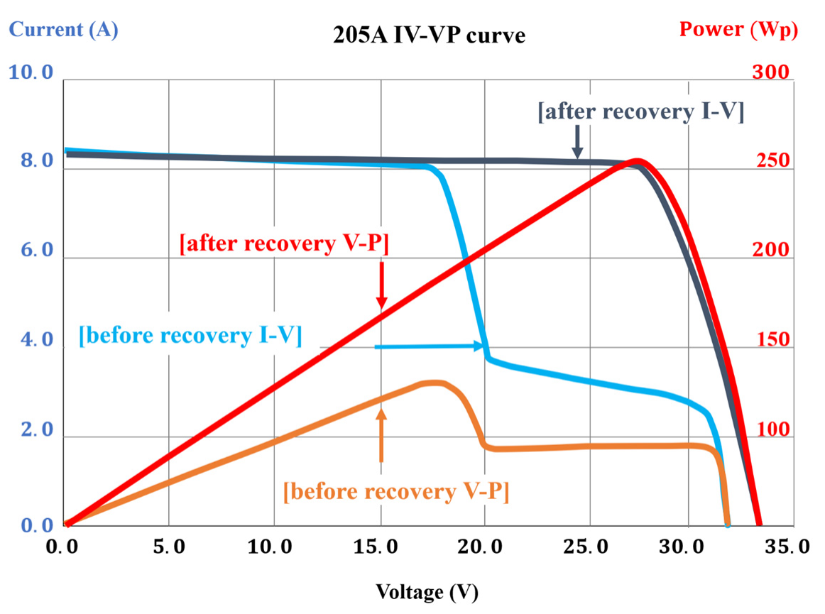
Figure 10 shows a comparison of the I–V and voltage–power (V–P) curves before and after the recovery of the 205A sample.
Earlier, the experiment indicated that the short-circuited bypass diode of the 205A sample should be replaced when measuring power, because the diode was damaged and had a small resistance; the simulator recognized the module as 36 series of four strings, not 54 series of six strings. As a result, even if the electrical power was almost the same during the simulation, Voc appeared differently; thus, the fill factor was distorted as if it were a normal module in the 36 series of four strings. However, it was a module that had a short-circuited diode with six strings. Therefore, it was necessary to convert it to a normally operated bypass diode and measure the electrical data.
Figure 11 shows the I–V curve of the 205A sample before and after replacing the short-circuited bypass diode.
Table 5 shows the electrical data measured when the 205A sample had a short-circuited diode and changed to a normal diode before the above recovery.
The module power output and current values were almost the same as the two data; however, as mentioned earlier, if the bypass diode is short-circuited, it will not be able to read the
Voc of the shorted string. Therefore,
Voc was 22.66 V, which was approximately 31.3% lower than the
Voc value of 32.98 V in a normal diode. Thus, the fill factor value was 0.701, which did not properly reflect the power decrease in the initial module and is distorted. Therefore, to remove variables outside the module, such as diode failure, and understand the damage characteristics of the module in the state of the module damaged by the RSB hotspot, electrical characteristics should be identified after replacing the damaged diode. This is the same as the #3 diode of the 240B sample, which did not have an EL image of strings #5 and #6.
Table 6 compares the initial, failed (before recovery), and electrical data for the 240B and 240C samples.
The 240B and 240C samples were recovered at 233.7 and 231.9 Wp, respectively, to 97.38% and 96.63% of the rated power, respectively, and recovered to a level slightly beyond the normal tolerance of ±3% of the new modules. Therefore, we concluded that the recovery results were not significantly different between factory and on-site recovery.
Figure 12 shows an EL image before and after the recovery of the 240B sample module where the RSB hotspot occurred owing to poor soldering.
In the recovery process, without removing the back sheet and lamination process, a process of punching and re-soldering a hotspot part using iron, filling the part with silicon resin, and finishing it with sealant and back-sheet tape was used. In this process, the technical difference was that the insulation layer was recovered using punching and resin of iron without a process such as removing the back sheet or re-lamination used to recover the power of the 205 A sample.
Figure 13 shows a comparison of the I–V and V–P curves before and after the recovery of the 240B samples whose output was recovered.
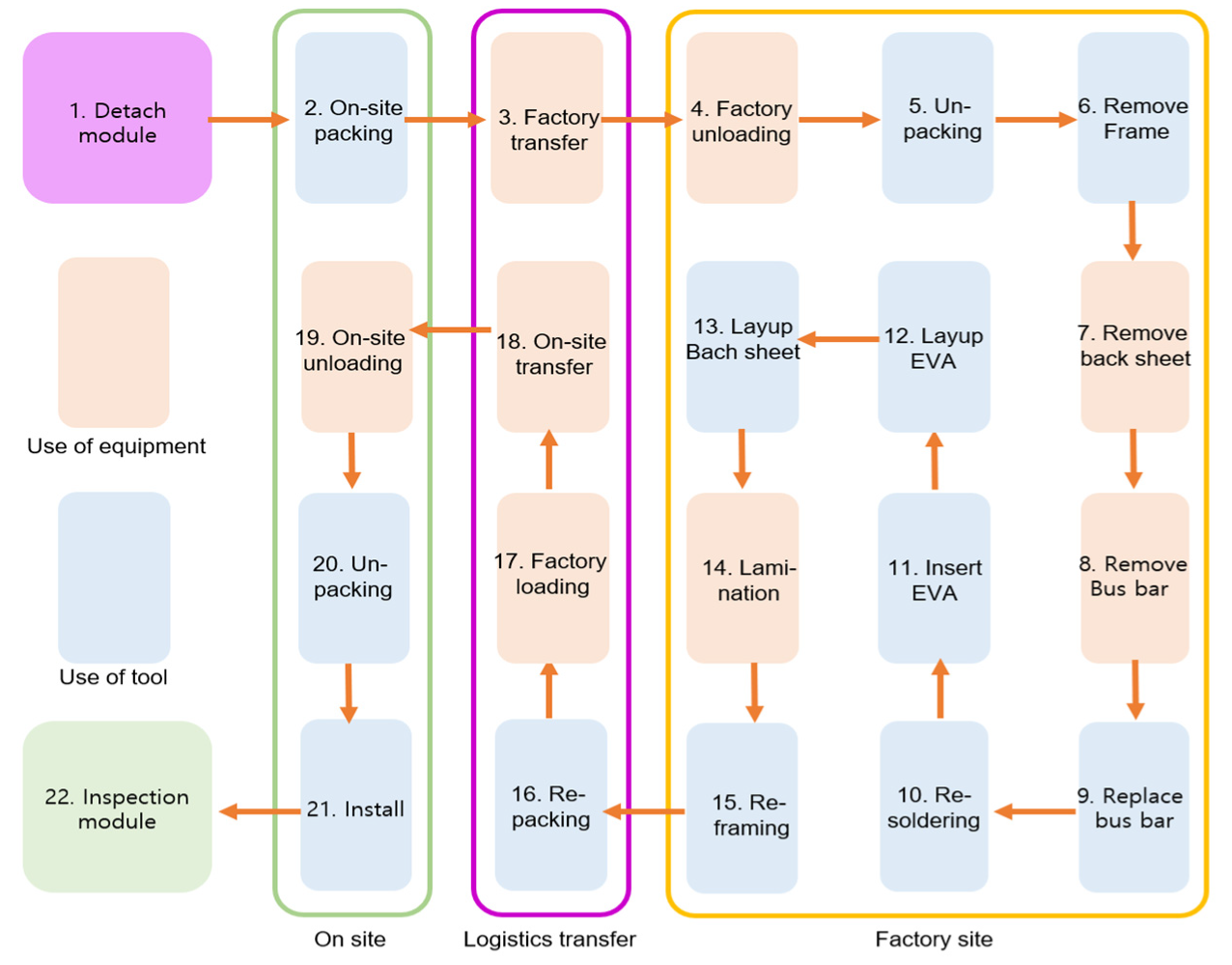
Figure 14 schematically shows the factory recovery process used to recover the 205A module. Although the RSB hotspot was recovered close to its rating, approximately 22 processes were consumed from module collection to post-installation inspection, even if the use of the equipment was reduced as much as possible. The lack of recycling plants for waste solar modules has location problems and economic problems, but the economic feasibility caused by the high cost of collecting modules may be the reason [
59,
60]. The process indicated in red in the figure is one in which equipment must be used, and the equipment is used not only for the recovery process of the module, but also for the logistics transfer, and loading and unloading of the module before and after repair. If RSB hotspots occur in an operating plant, the economic loss is significant, because of the energy and cost required in the recovery process as well as the loss of power generation in the recovery module due to time delay.
In the process shown in
Figure 15, only a slight difference occurs in power recovery, even if the equipment is not used in the factory and only tools are used in the field. All processes are performed on-site, and after the module is restored, it can be installed on-site and inspected immediately, without repacking or transfer processes. Overall, the process of reinstalling and inspecting through 22 steps in factory restoration is reduced to eight steps, reducing the time and cost. The greatest advantage of on-site recovery is that the loss of power generation time of the most important modules mentioned above can be minimized if they are recovered by rolling them in the field. After re-soldering the upper and lower bus bars of the 240B module using on-site recovery technology and replacing the bypass diode, the RSB hot spot was also recovered by poor soldering of strings and cells. The 240C module was also recovered using the same process. Through a comparison of the technology completeness owing to the difference between the module factory recovery and on-site recovery process with recovery data, no significant difference was observed. Module 205A recovered almost to the rated level (<1%), but 240B and 240C were slightly different; therefore, we determined that the initial power was assumed to be the rated power and calculated. Because 240B was recovered within the product tolerance value, only a slight power degradation occurred, and the exact initial power was not known, but for 240C, assuming that the actual initial power was 232.8 Wp, which was the lower limit of tolerance, we observed that it recovered close to −0.04%. None of the three samples recovered from the stomach were observed to have remarkable long-term degradation. As a result of the above experiment, no remarkable long-term degradation was observed in any of the three samples. Finally, compared with the reliability of factory recovery technology that has already been verified, the long-term reliability of the on-site recovery process using resin with EVA by punching was verified using a thermal cycle (TC) 200 test.
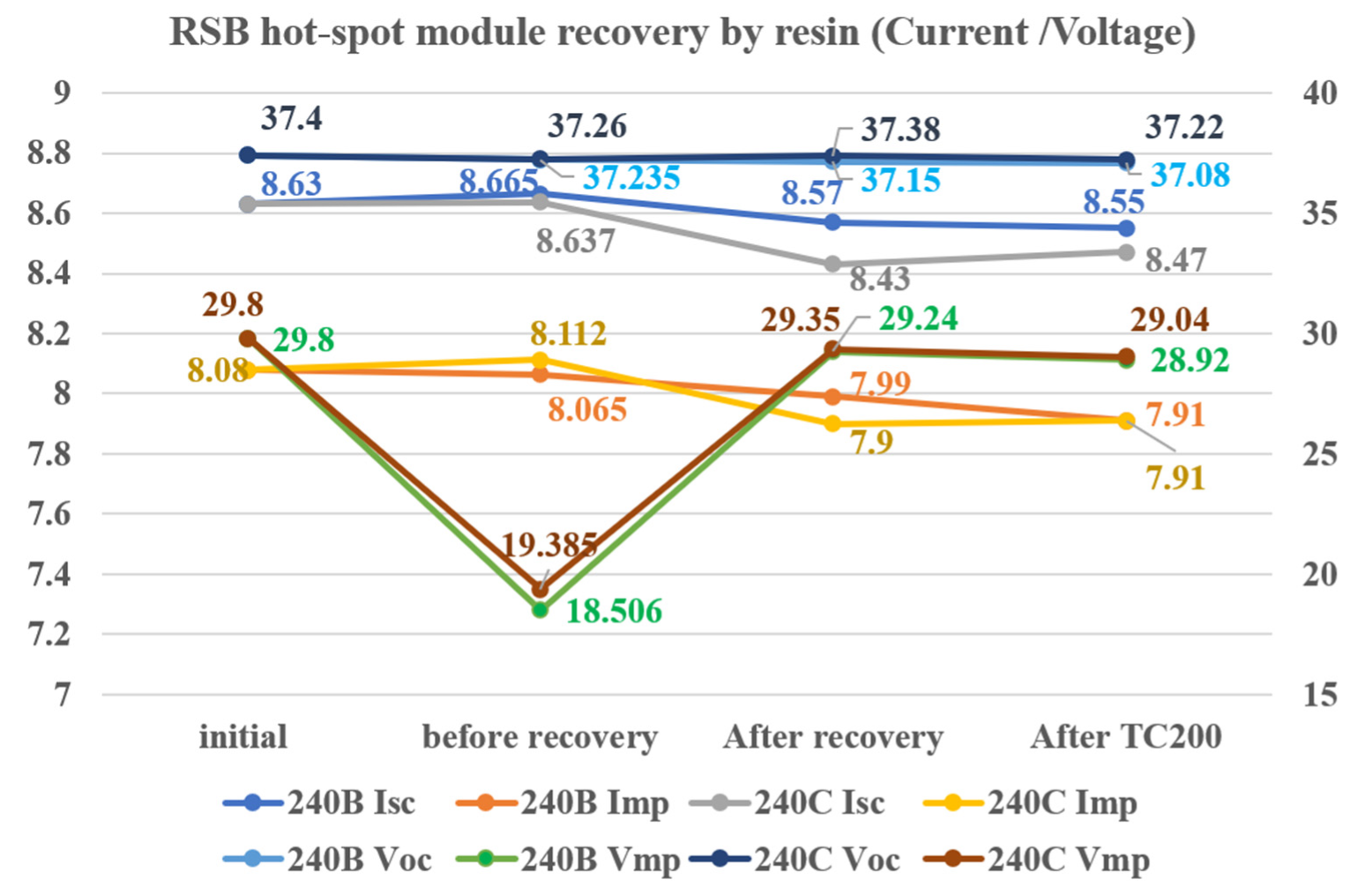
Table 7 presents the results of evaluating the long-term reliability after the TC 200 test. The TC 200 test results after on-site recovery of the 240A and 240B samples indicated a change in values of −5.0 and −2.2 Wp, respectively, which were reduced by −2.14% and −0.95% from the values before the TC 200 test, respectively. After the TC 200 test, the maximum allowable Pmax degradation is −5%, and the experimental results were within the certification test criteria of the new fabrication module.
Figure 16 shows a graph of the Pmax change of the RSB hotspot module using the on-site recovery method. As previously stated, the bypass diode was damaged by the RSB hotspot, and both samples lost power outputs of −38.01% and −34.69%, respectively, compared with the rated power before recovery. Subsequently, the power output was recovered to −2.94% and −3.69% compared with the rated power through re-soldering using a back-sheet punching and recovery process using resin. To verify the long-term reliability of the recovery method, we performed a TC 200 test, and the power output results were measured as −2.14% and −0.95%, which are within –5%.
Figure 17 shows a graph that summarizes the values measured through step-by-step experiments from the initial rated power and compares the power output before and after recovery and after the TC 200 cycle test with each electrical value. An unusual observation in the recovery steps of the RSB hotspot module was that the
Isc values varied only slightly step by step, and the
Imp and
Voc values exhibited only slight changes when hotspots occurred, after recovery, and after reliability testing, but not to the extent of a power change. The factor directly correlated with the power change was
Vmp, which accurately matched the power change pattern of the module step by step.
4. Conclusions
This study analyzed the power loss caused by damage to the bypass diode through the EL image and the I–V and V–P curves of the module as a result of the RSB hotspot caused by poor soldering between the bus bar and the interconnector in the module. The same power as the initial power of the module was recovered. Damage to the bypass diode caused by RSB hotspots results in a large power loss of more than 30% in the unit module, which is one of the most economical module recovery methods owing to its simple recovery technique. The module recovered from the RSB hotspot almost to the rated power level, although it had been operating in a plant for many years. An important change is the application of on-site recovery technology using simple tools to improve the factory recovery technology using various types of equipment. The on-site recovery technology of the back sheet punching method and insulation with resin instead of the back sheet removal and lamination process was verified for reliability through the TC 200 cycle test. Through this process change, a recovered module can be reused after seven steps instead of the current 22-step recovery process. Note that toluene and xylene contained in silicon resin may soften EVA that is not crosslinked, even at room temperature; thus, the influence on EVA should be minimized by removing the organic solvent as quickly as possible under ventilation conditions. The sample used in this experiment was collected at a plant site after heat generation was confirmed using an IR camera, and the power loss occurred in a string of approximately 33%; thus, the power loss was approximately −37% in the 205A sample, −38% in the 240B sample, and approximately −35% in the 240C sample. The 205A sample was recovered using factory recovery, and the 240B and 240C samples were recovered using the on-site recovery method, recovering power to −0.82%, −2.94%, and −3.69%, respectively, compared with the rated power. The 240B and 240C output degradations after the TC 200 cycle test performed for long-term reliability verification of on-site recovery methods were measured at −2.14% and −0.95%, respectively. Note that Isc exhibited a slight change even when the RSB hotspot occurred and power was degraded, and Vmp and Imp exhibited slight changes, but the largest changes were Vmp and the fill factor. The reason Isc and Voc are similar is that in the I–V and V–P curves, the starting and ending points of a normal curve are almost similar to those of a curve in which a diode operates owing to the RSB hotspot. Thereafter, the hotspot curve exhibits a small peak at a position faster than a normal curve, and when reverse current occurs, current and power decrease rapidly, and then flatly progress along the voltage axis in the form of a step in the middle and end at a Voc value. Naturally, Vmp and the fill factor recovered most prominently after the module power was recovered. When the technology development of photovoltaic modules reduces the valuable resources that can be recycled from waste modules, considering environmentally and economically, the most desirable method of recycling a photovoltaic module at the end of its commercial life is a technology that recovers power to enable the module to be used again.


