Article

A New Multilevel Inverter Topology with Reduced DC Sources

1
Department of Electrical and Computer Engineering, King Abdulaziz University, Jeddah 21589, Saudi Arabia
2
Center of Research Excellence in Renewable Energy and Power Systems, King Abdulaziz University, Jeddah 21589, Saudi Arabia
3
Switchgear Electromechanical, Chennai 600082, India
4
Department of Electrical and Electronics Engineering, SRM Institute of Science and Technology, Kattankulathur Campus, Kattankulathur 603203, India
5
Renewable Energy Lab, College of Engineering, Prince Sultan University, Riyadh 11586, Saudi Arabia
6
Power Electronics and Renewable Energy Research Laboratory, Department of Electrical Engineering, University of Malaya, Kuala Lumpur 50603, Malaysia
7
School of Software and Electrical Engineering, Faculty of Science, Engineering and Technology, Swinburne University of Technology, Victoria, VIC 3122, Australia
8
Electrical Engineering Department, United Arab Emirates University, Al Ain 15551, United Arab Emirates
9
National Water and Energy Center (NWEC), United Arab Emirates University, Al Ain 15551, United Arab Emirates
*
Authors to whom correspondence should be addressed.
Energies 2021, 14(15), 4709; https://doi.org/10.3390/en14154709
Submission received: 15 June 2021 / Revised: 21 July 2021 / Accepted: 24 July 2021 / Published: 3 August 2021

Abstract

:
The component count for the multilevel inverter has been a research topic for the last few decades. The higher number of power semiconductor devices and sources leads to a higher power loss with the complex control requirement. A new multilevel inverter topology employing the concept of half-Bridge modules is suggested in this paper. It requires a lower number of dc sources and power components. The inverter is controlled using a fundamental frequency switching scheme. With the basic unit being able to produce 13 level voltage waveforms with three dc voltage sources, higher-level inverter configuration has also been discussed in the paper. The performance of the topology is analyzed in the aspects of circuit parameters and found better when compared to similar topologies proposed in recent literature. The comparison provided in the paper set the benchmark of the proposed topology in terms of lower component requirements. The topology is also optimized with two voltage fixing algorithms for maximizing the number of levels for the given number of IGBTs, drivers and dc sources, and the observations are presented. The efficiency analysis gives the peak efficiency as 98.5%. The simulations were carried out using the PLECS software tool and validated using a prototype rated at 500 W. The results with several test conditions have been reported and discussed in the paper.

1. Introduction

Multilevel Inverters have been extensively used in the applications like FACTS, Electrical Vehicles, Smart grids etc., due to their merits like low dv/dt stress, modularity, improved power quality. These applications are due to their ability to synthesize high terminal voltages with low and medium voltage devices [1,2]. Conventionally, multilevel inverters are grouped under three major categories viz., Diode Clamped or neutral point clamped Multilevel Inverter (DC-MLI) or NPC-MLI, Flying Capacitor Multilevel Inverter (FC-MLI) and Cascaded H-Bridge Multilevel Inverter (CHB-MLI). As far as the number of power components are concerned, DC-MLI requires numerous diodes when the number of levels in the waveform increases which makes the circuit control tedious. In FC-MLI, the voltage balancing issue posed by the diodes of NPC-MLI can be resolved using the redundant switching states offered by the clamping capacitors; but a higher number of passive components in the circuit will be a threat to circuit reliability [3,4]. CHB-MLI is highly modular and relatively simpler to control in comparison with the other two topologies. Further, it does not require any voltage balancing circuits as it employs independent dc sources [5,6,7]. Nevertheless, in conventional CHB-MLI, the required number of power switches increases by four for any additional dc source. The requirement for higher number of power devices in the conventional topologies have paved the way for research in Multilevel inverter topologies with reduced device count [8,9].
Most of the topologies utilizing independent dc sources for level synthesis are based on the idea of using switched dc sources for level addition and an H-Bridge for polarity reversal [10,11]. A modified H-Bridge, so-called developed H-Bridge, is proposed by [12]. The H-Bridge of this topology has six switches instead of four and two independent dc sources per module. The level addition can be done by cascading this developed H-Bridge. The topology requires a minimum of two sources and the total blocking voltage will increase rapidly if the number of H-Bridges increases. A new cascaded structure with its basic sub-module comprising of independent switched dc sources for level synthesis and an H-Bridge is analyzed in [13]. However, all the switches connecting the dc sources are bidirectional switches. This increases the number of components and the total blocking voltage across the H-Bride is four times the dc voltage. Across connected multilevel inverter topology with the switched dc sources connected in a crisscross fashion is suggested by [14]. In this, the required number of switches increases by three for any additional independent source. This is 25% less when compared to conventional CHB-MLI, but the number of components is still high for a higher number of levels. A new multilevel inverter topology is discussed in [15]. It requires n + 5 switches for ‘n’ independent sources. However, the blocking voltage across the switches in the polarity changer is very high when the levels in the terminal voltage waveform increase. This necessitates switches with a higher voltage rating and heavier heat sink. A three-phase hybrid multilevel inverter topology is presented in [16]. The voltage balancing is achieved by letting the topology operate in selective switching states using the space vector modulation technique. This makes the control a bit complex and tedious task. All the above-mentioned topologies are symmetrical topologies, wherein the magnitude of all the dc voltage sources in the circuit will be equal. Asymmetrical operation is another solution that is often considered to reduce the switch count in MLI topologies. In [17], an E-type module for asymmetric multilevel inverter topology is proposed where the basic unit requires at least four independent dc sources. The topology proposed in [14] utilizes four-quadrant switches to make the circuit capable of operating in symmetrical and asymmetrical mode. In the topology presented in [18], the number of switches in the conduction path is high resulting in higher losses. However, the usage of capacitors in the circuit will necessitate separate voltage balancing methods. In the ST-type module discussed in [19], the total blocking voltage of the module is very high as few of the switches are supposed to block thrice the input voltage. An asymmetric dual-source multilevel inverter topology is proposed by [20], here the level adder comprises only two independent sources. The level addition is achieved using the clamped capacitors across the sources. Even though the required number of switches is reduced drastically at higher number of levels, the voltage balancing circuit used in the circuit makes it bulky and tedious to operate. The switches to level ratio are relatively high in the novel cross-connected multilevel inverter topology proposed by [21]. The higher number of switches makes this circuit impractical. All the topologies discussed above have a common issue of higher device count [22,23,24,25,26,27,28].
A new hybrid multilevel inverter topology combining the concept of hybrid and asymmetric operation is proposed in this paper. The lower number of the components has been the main design aspect for the proposed topology. The lower number of devices and sources enables the topology for the applications related to solar PV and motor drives. The salient features of the proposed topology are as follows.
  • The basic unit of the proposed topology generates a 13 level output voltage with a higher number of levels is possible with the generalized structure.
  • A reduced voltage stress is achieved and lower number of dc voltage sources is required.
  • Lower number of switching transitions improves the efficiency of the proposed topology.
  • The 13 level basic unit has been discussed in detail and has been validated using a 500 W experimental setup.
The remaining part of the paper is organized as follows. Section 2 explains the structure and operation of the topology along with the comparison of the proposed topology with the other recent topologies in the literature in the aspects of the number of switches required and number of sources required for the required number of levels. Section 2 also deals with the modulation technique and efficiency estimation along with the selection of magnitude of dc voltage sources of the extended structure of the proposed topology and its optimization. Section 3 gives the simulation and experimental results, and the conclusion of the paper is provided in Section 4.

2. Methodology

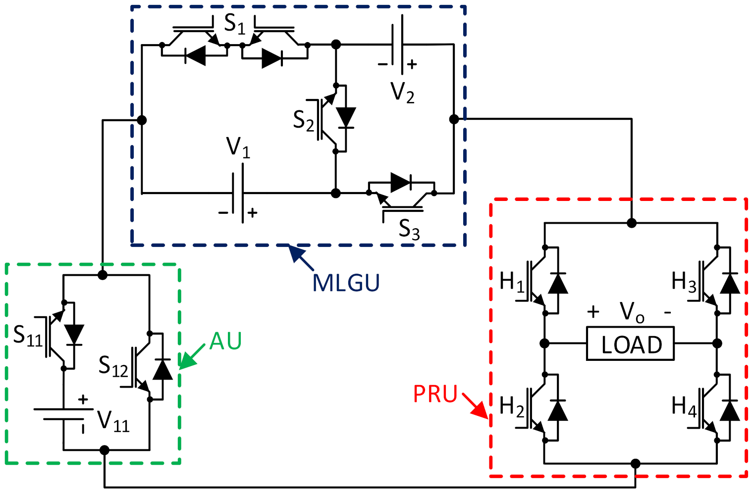
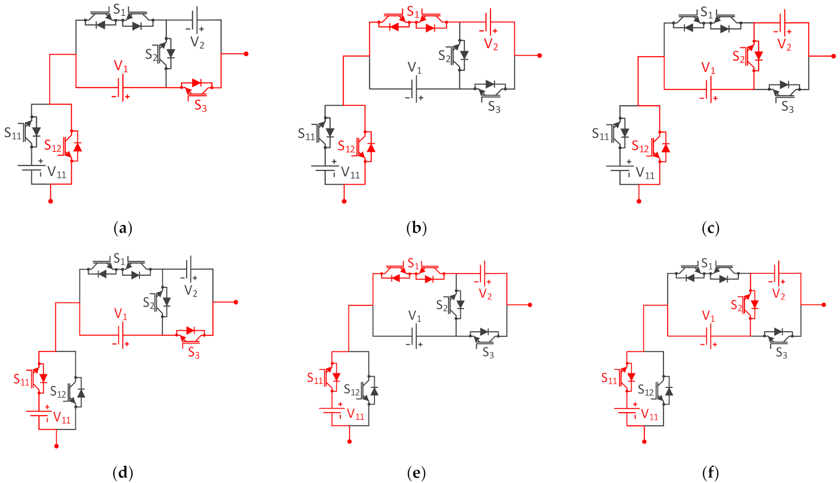
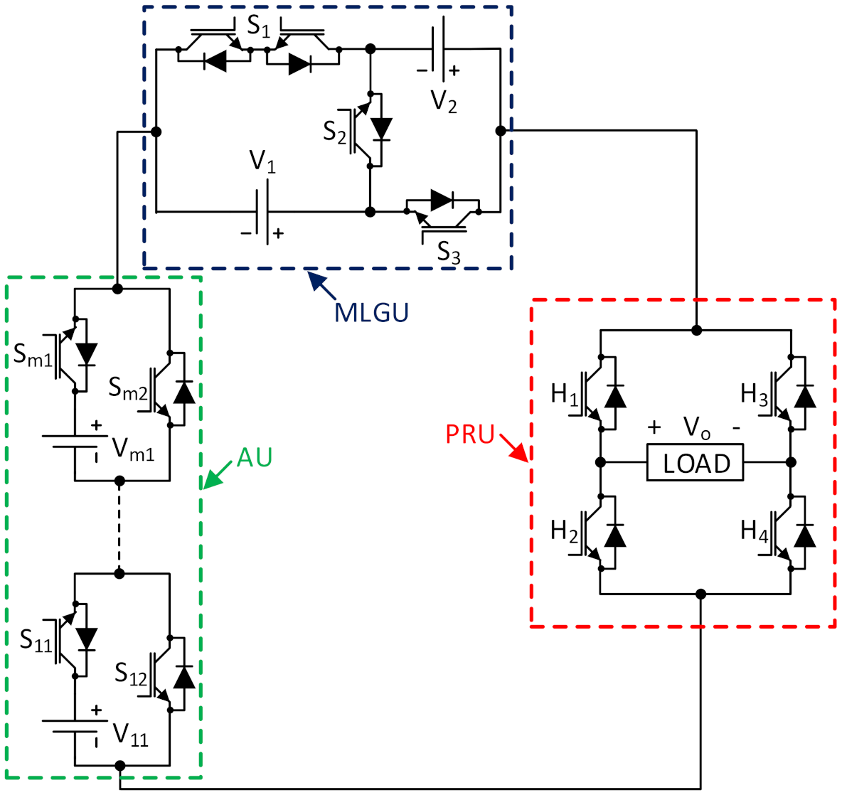
2.1. Description of the Proposed Topology

The basic unit of the proposed hybrid multilevel inverter topology is shown in Figure 1. The basic unit consists of three parts: 1. Main Level generation Unit (MLGU), 2. Auxiliary Unit (AU) and 3. Polarity Reversal Unit (PRU). The MLGU consists of one bidirectional switch S1, two unidirectional switches S2 and S3 along with two dc voltage sources V1 and V2. The MLGU can generate three different voltage levels i.e., V1, V2, and V1 + V2. In the MLGU, only one switch should be turned ON at a time otherwise the dc voltage sources will short-circuit. Since the switches of MLGU need to be operated at a higher frequency, the magnitude of V1 and V2 should be selected as low as possible.
The auxiliary unit consists of two unidirectional switches S11 and S12, supplied from a dc voltage source V11 which makes a half H-bridge circuit. One AU can generate two voltage levels with zero and V11 magnitude. Both switches S11 and S12 should be operated in a complementary mode to avoid short-circuiting of voltage source V11. Figure 2 shows the connection diagram for all the possible switching combinations of the AU and MLGU modules. The AU and MLGU can produce six voltage levels as shown in Figure 2a–f. For each voltage level, it can be seen that only two switches are operated, except for voltage levels shown in Figure 2b,e. In these two voltage levels, the number of conducting components becomes three due to the use of the bidirectional switch. The lower number of conducting switches reduces the overall losses. Also, the switched of AU are turned on and off only once in a positive or negative half cycle, this further reduced the losses.
The combination of MLGU and AU generates the voltage levels in positive polarity only. To generate both positive and negative voltage polarities including zero voltage levels, PRU is used, which is a conventional H-Bridge circuit employing four unidirectional switches (H1–H4). The combination of all these three units results in generating 13 levels at the output. The number of auxiliary units connected in series with the MLGU can be increased as shown in Figure 3 if the required number of levels in the terminal voltage is higher. The switching states for the generalized topology with ‘m’ auxiliary units connected in series is shown in Table 1. For the given ‘m’ auxiliary units, the number of levels in the terminal voltage wave can be estimated as follows
N L e v e l = N = 3 × 2 m + 1 + 1
The number of switches required to construct the topology with ‘m’ auxiliary units Nsw can be estimated as
N s w i t c h = 2 m + 8
Since one of the switches in MLGU is a bidirectional switch with two IGBTs, the switch can be controlled with a single driver. Therefore, the number of drivers required for the generalized structure can be found as
N d r i v e r = 2 m + 7

2.2. Comparative Study

The reduction in the number of switches and dc voltage sources while achieving a higher number of levels is the main objective of the proposed topology. The components required along with the cost of the topology are compared with the similar topologies available in the literature and the observations are presented in Table 2. From Table 2, the following observations are made, even though the topology given in [13] requires only 10 IGBTs, the required number of independent sources is double the time of the proposed topology. The merits accrued due to the lesser number of IGBTs in [17,20] are overshadowed by the inclusion of capacitors. The inclusion of capacitors in the circuit will make the circuit control tedious and require additional voltage balancing circuitry. Despite the fewer IGBTs employed in the above topologies, the total cost of the proposed topology is relatively low at 66.75 USD when compared to the topologies found in recent literature.

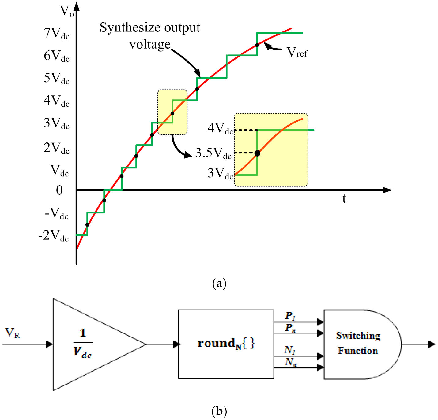
2.3. Modulation Technique

Multilevel inverters can be controlled using both high and low-frequency switching schemes. Each scheme has its merit and demerit [29]. To control the proposed topology, a fundamental frequency switching scheme is used. The Space Vector Modulation (SVM) scheme or selective harmonic elimination scheme can be used for fundamental frequency switching. The control complexity in SVM makes it less attractive. As far as the selective harmonic elimination scheme is concerned, if the number of levels in the stepped voltage waveform increases, it will become tedious to solve the equations to determine the switching angles precisely [30,31,32,33]. In this paper, the nearest level modulation scheme is used. The control method is shown in Figure 4. In this method, the reference sine wave with fundamental frequency is compared with constants to realize each switching state. If the voltage waveform has ‘n’ steps in the positive half cycle of the voltage waveform, then ‘n’ constants have to be compared with the sine wave rated 6 per unit (p.u). The value of the nearest level constant is to be chosen from 0 to 1. Then, the nearest level constant will be added to the level number of the previous level to get the constant to be compared with the reference to synthesize the succeeding level s shown in Figure 4a. The pulses generated by comparing the nearest level constants with the reference are then used to trigger the IGBTs according to the switching function shown in Figure 4b.
For example, the gate pulses to the switches conducting in level 1 have to be generated by adding the chosen nearest level constant to zero. After analysis, many authors have concluded that 0.4 will be the optimum nearest level constant because the THD and magnitude of lower order harmonics will be very low at that point [23,24,25]. The switching angle for each level can be estimated as
θ x = x 0.6 N , x = 1 , 2 , 3 , N
Using (4). In the equation, the value 0.6 is obtained by subtracting the nearest level constant from 1.

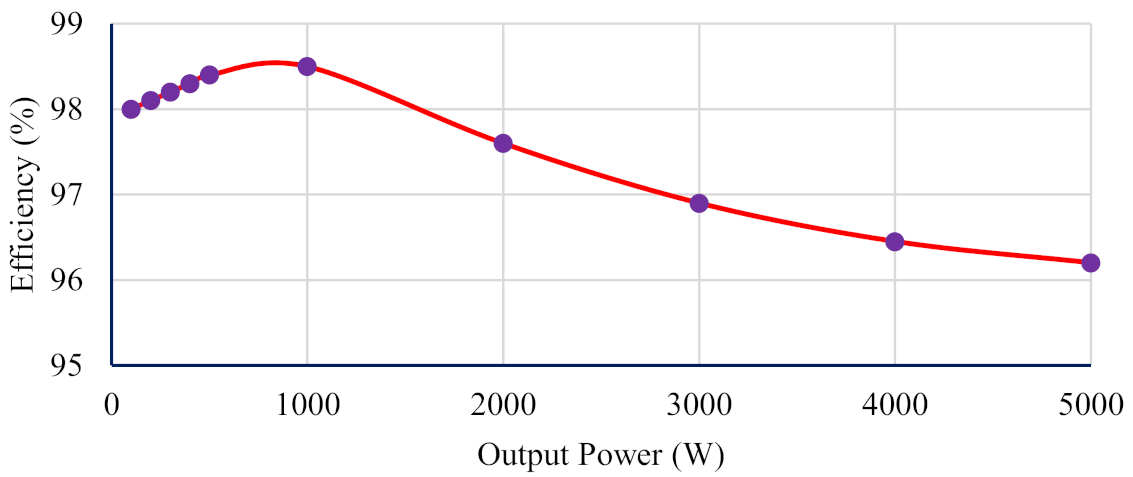
2.4. Efficiency Estimation

In this section, the theoretical loss calculation is presented to calculate the efficiency of the proposed inverter topology. The major losses associated with the cascaded H-Bridge inverter system fed by independent dc sources are conduction and switching losses [26]. The estimation is performed by assuming that the load is purely resistive and the voltage available at the inverter output terminal is staircase waveform [27].

2.4.1. Conduction Loss

The conduction loss in a multilevel converter occurs when IGBT switches are turned ON and conducting current. For the proposed inverter topology, the losses incurring in each of the IGBT switches employed in the polarity conversion unit, MLGU and Auxiliary units are estimated separately for calculating total conduction loss. In the proposed Inverter, H-Bridge is used as a Polarity conversion unit in which two IGBTs (either H1 & H4 or H2&H3) are in load Current path at any instant of time. In this case, the conduction loss for the quarter of the fundamental cycle is obtained by
P C o n , H = 4 π 0 π 2 I L 2   ( t ) R o n , T d t
where R o n , T and I L t   are the transistor on-state resistance and load current, respectively. The load current can be assumed to be sinusoidal if the proposed topology generates a higher number of output voltage levels by connecting a greater number of auxiliary units. Therefore, the load current can be written as
I L = I P sin w t
Using (5) and (6), the average conduction loss of the H-Bridge is obtained as below
P C o n , H = 4 π 0 π 2 I p 2     s i n 2 w t R o n , T   d t
For the auxiliary unit, one unidirectional IGBT switch is in conduction throughout the fundamental cycle. For the period of   π 2 , the loss in AU is calculated as
P C o n , A u x = 2 π 0 π 2 I p 2     s i n 2 w t   R o n , T   d t
For m auxiliary units, the conduction loss is calculated as given below
P C o n , A u x ,   T o t a l = m × P C o n , A u x
where m = 1,2…
The MLGU contains a bidirectional switch (S1) and two unidirectional switches (S2 & S3). The MLGU bidirectional switch is used only to synthesize voltage from V2 source, during that time one IGBT and one diode of the bidirectional switch (S1) is in the conduction path. Out of the two unidirectional switches either S2 or S3 are in conduction through the fundamental cycle. The conduction loss for the MLGU can be obtained by
P C o n , M L G U = 2 π 0 π 2 I p 2     s i n 2 w t   R o n , T   d t + t 2 t 3 I p 2     s i n 2 w t   ( R o n , T + R o n , D ) d t + t 5 t 6 I p 2     s i n 2 w t   ( R o n , T + R o n , D ) d t
The total conduction loss for the full cycle of the output waveform can be obtained from Equations (7), (8) and (10). Because of the quadrant symmetry of the output voltage waveform, the conduction loss is estimated for the period of the quarter cycle and the result is multiplied by four to find the average conduction loss
P C o n , T = 4 × 1 2 π P C o n , H + P C o n , A U + P C o n , M L G U

2.4.2. Switching Loss

In IGBT switches, during the transition from on state to off state or vice versa, the switching loss occurs due to the overlapping of voltage and current. The energy loss during turn on and turn off period of the IGBT switches is obtained as follows
E O N = V O N I 6 t o n
where VON, I, ton are the IGBT on-state voltage, the current through IGBT after turning on and turn on time respectively
E O F F = V O F F I 6 t o f f
where VOFF, IOFF, toff are IGBT off-state voltage, the current flowing through IGBT before turning off and turn off time respectively. Equations (12) and (13) are used to estimate the average switching power loss in the proposed topology and it is calculated for switches in each unit separately. In PCU, there is one turn ON and one turn Off of the IGBT switches for half period of the fundamental cycle, and switching loss in PCU is evaluated as follows
P s w , P C U = 2 × f × ( E O N + E O F F ) = 1 3 f × I × V O N t o n + V O F F t o f f
where f is the fundamental switching frequency. Similarly, for AU in total, there is one turn on and one turn off during the half period and the equation is equivalent to the one obtained for PCU which is given as
P s w , A U = 2 × f × ( E O N + E O F F ) = 1 3 × f × I V O N t o n + V O F F t o f f
The MLGU contains three switches and the number of transitions that happened in half cycle is found to be nine out of which six turn on and three turn off. The switching MLGU is obtained as follows,
P s w , M L G U = 2 × f × ( 6 E O N + 3 E O F F ) = f × I 2 V O N t o n + V O F F t o f f
The total switching loss for a full cycle can be calculated as
P s w , T = f × P s w , P C U + P s w , A U + P s w , M L G U
The total power loss and the efficiency of the proposed inverter are calculated by using (11) and (17)
P L o s s , T = P C o n , T + P s w , T η = P o u t P i n + P L o s s , T
Based on the above formulation, the efficiency of the proposed topology has been estimated and is shown in Figure 5. For the estimation of the efficiency of the proposed topology, the data of TOSHIBA IBGT GT50J325 switch has been used with varying output power. As indicated from Figure 5, the peak efficiency of the proposed topology is 98.5% at an output power of 1000 W. For higher output power, the efficiency decreases, however, the drop is not significant as at 5 kW, the efficiency is 96.2%.

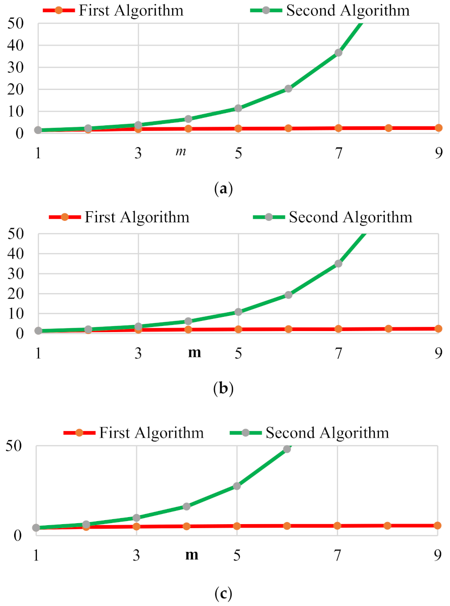
2.5. Algorithms to Fix Voltage Magnitude in Extended Topology

The effectiveness of the topology depends on the ability to generate a greater number of levels and maximum voltage at its output terminal by utilizing fewer IGBT switches along with the associated driver circuits. The auxiliary unit’s source voltage is predicted using two proposed algorithms based on the generation of maximum voltage and more numbers of levels with less number of power components. The number of switches used in each of the AU has to be constant to obtain the maximum number of levels and the equalities is given by
N 1 = N 2 = N 3 = = N
where N1, N2, … Nm is the number of switches in the first, second up to ‘m’ AU modules connected in series to increase the output voltage level.

2.5.1. First Algorithm

In this algorithm, the auxiliary units (AU) dc source voltage at all the stages are equal and it is equal to 3V1
V 11 = V 21 = = V m 1 = 3 V 1
Stage 1:
When Single AU is connected to the MLGU, the maximum output voltage value and number of levels are obtained as follows
V o , 11 m a x = 2 ( N 1 + 1 ) V 1
N L , 11 = 6 N 1 + 1
Stage 2:
On connecting the second AU, the maximum output value and levels are found as follows
V o , 21 m a x = 3 ( N 2 + 1 ) V 1
N L , 21 = 9 N 2 + 1
For the mth stage, the maximum voltage and the maximum number of levels in the voltage waveform can be obtained by using the Equations (19) and (21)–(24)
V o F , m 1 m a x = ( m + 1 ) ( N + 1 ) V 1
N L F , m 1 = 3 N ( m + 1 ) + 1  

2.5.2. Second Algorithm

In the second algorithm, each of the AU dc source values is different and the dc source value to obtain maximum output voltage and the maximum number of levels can be derived as follows
Stage 1:
The dc source magnitude of the first AU connected is given as
V 11 = ( N 1 + 1 ) V 1
The maximum voltage and number of levels in this stage are found as follows
V o , 11 m a x = 2 ( N 1 + 1 ) V 1
N L , 11 = 6 N 1 + 1
Stage 2:
The second AU dc source voltage magnitude connected is given
V 21 = 2 ( N 2 + 1 ) V 1
The corresponding maximum voltage and levels obtained during this stage are
V o , 21 m a x = 4 ( N 2 + 1 ) V 1
N L , 21 = 12 N 2 + 1
For ‘m’ AU’s, the equations can be obtained using the Equations (19) and (27)–(32)
V m 1 = m ( N + 1 )
V o S , m 1 m a x = 1 2 m 2 + 1 2 m + 1 ( N + 1 ) V 1
N L S , m 1 = 3 ( N m + 1 ) + 1
where V o S , m 1 m a x & N L S , m 1 are the maximum output voltage and the maximum number of levels synthesized using the second algorithm.

2.6. Optimization of Structures

The optimization of the proposed topology in terms of number of IGBTs, number of driver circuits, and number of dc sources required to synthesize the maximum number of levels for both algorithms are related by considering various aspects is presented below
The number of IGBT ( N S W )   in the proposed topology is obtained by
N S W = ( N 1 + N 2 + + N m + 8 )
For m stages, the number of IGBT required can be estimated as
N S W , m = i = 1 m N i + 8 = N m + 8
The Equations (25), (26), (34) and (35) can be used to find the relation between levels and various circuit parameters and the same can be used to determine the optimal structures with which the maximum number of voltage levels can be obtained with a minimum number of IGBTs drivers and dc sources.

2.6.1. Optimization of the Proposed Cascade Converter for Maximizing the Number of Levels with Constant Power Switches

By using Equations (26), (35) and (37) the topology is optimized to obtain a maximum number of levels with a constant number of IGBT’s for the proposed algorithms. The number of levels obtained using the first and second algorithms is given as follows
N L F , m 1 = N S W , F × 3 N ( m + 1 ) + 1 N m + 8
N L S , m 1 = N S W , S × ( 3 N m + 1 ) + 1 N m + 8
Here N S W , F   and   N S W , S denote the number of switches in the first and second algorithms which is kept constant. If the ratios 3 N ( m + 1 ) + 1 N m + 8   & ( 3 N m + 1 ) + 1 N m + 8 are minimum for a value of ‘m’ value then the condition is favorable to generate more levels with a constant number of switches. From Figure 6a, it is found that at m = 1 gives the optimal condition for both algorithms.

2.6.2. Optimization of the Proposed Cascade Converter for Maximizing the Number of Levels with Constant Driver Circuits

The maximum number of levels generated to the constant number of driver circuits for the first and second algorithm is given by Equations (40) and (41) and it is computed from Equations (3), (25) and (36)
N L F , m 1 = N D r , F × 3 N ( m + 1 ) + 1 N m + 7
N L S , m 1 = N D r , S × ( 3 N m + 1 ) + 1 N m + 7
The topology could able to generate more number of levels with constant driver circuits when the ratio’s 3 N ( m + 1 ) + 1 N m + 7 and ( 3 N m + 1 ) + 1 N m + 7 of the first and second algorithms are minimum. The minimum ratio value for both the algorithms are obtained when m = 1 and it can be seen from Figure 6b.

2.6.3. Optimization of the Proposed Cascade Converter for Maximizing the Number of Levels with Constant DC Sources

The relationship between the number of dc sources and the number of levels for the proposed algorithms can be, respectively, obtained by
N L F , m 1 = N D C , F × 3 N ( m + 1 ) + 1 m + N
N L S , m 1 = N D C , S × ( 3 N m + 1 ) + 1 m + N
It is evident from Figure 6c, m = 1 presents the optimal topology for generating more levels with constant Dc sources for both algorithms. The Equations (20)–(22) and Equations (23)–(25) provides the relation between the number of switches, number of drivers, and number of DC sources to the number of levels for the first and second algorithm respectively.

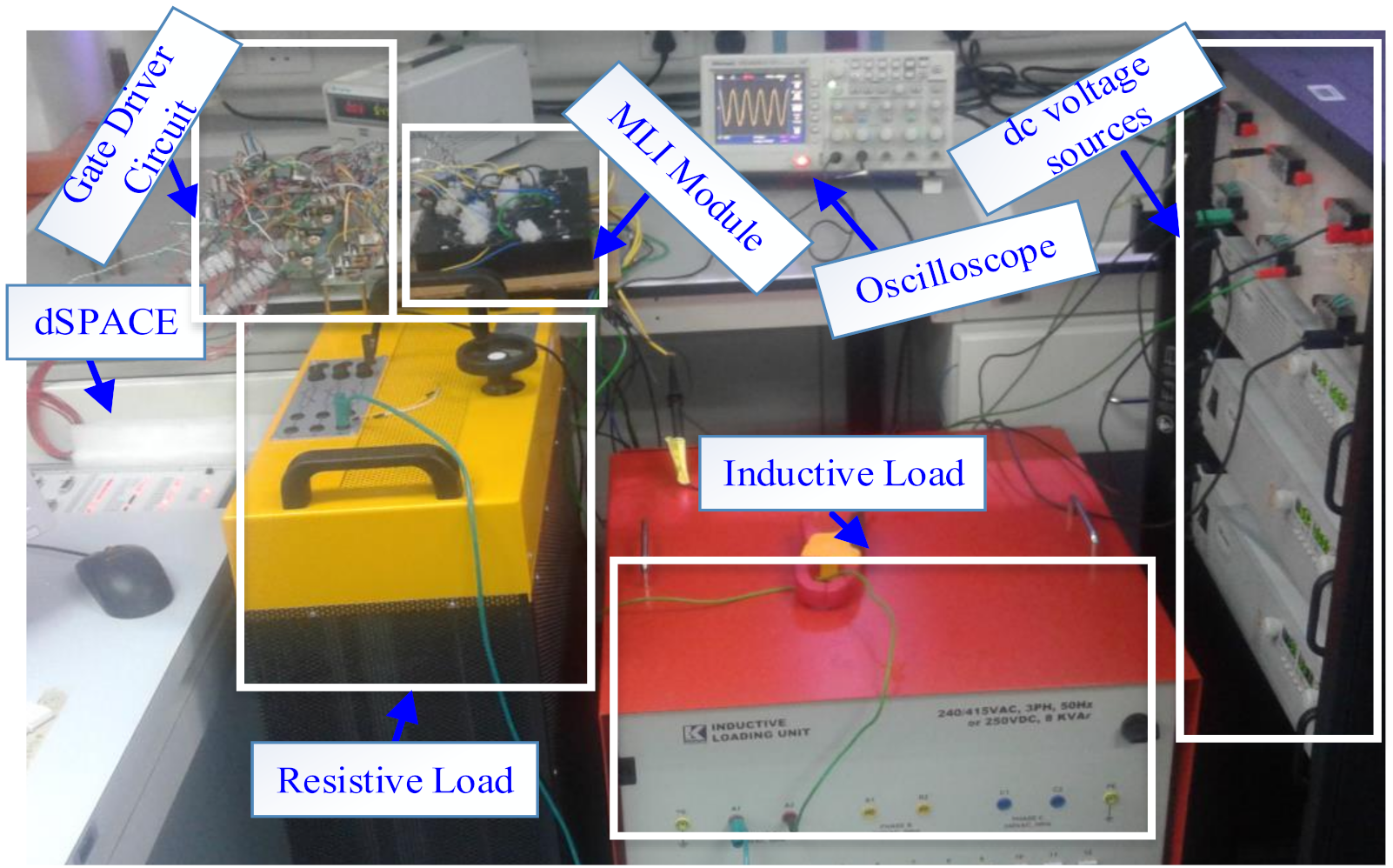
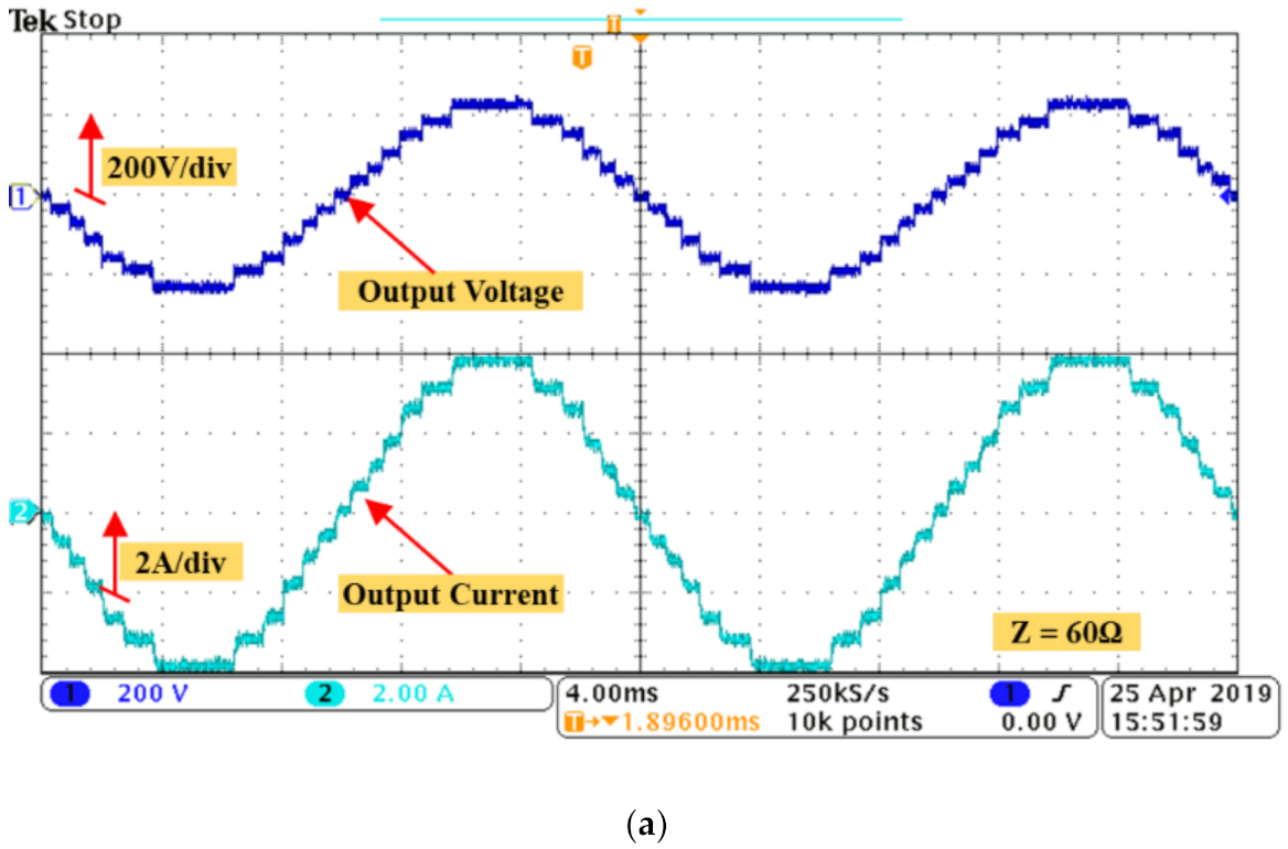
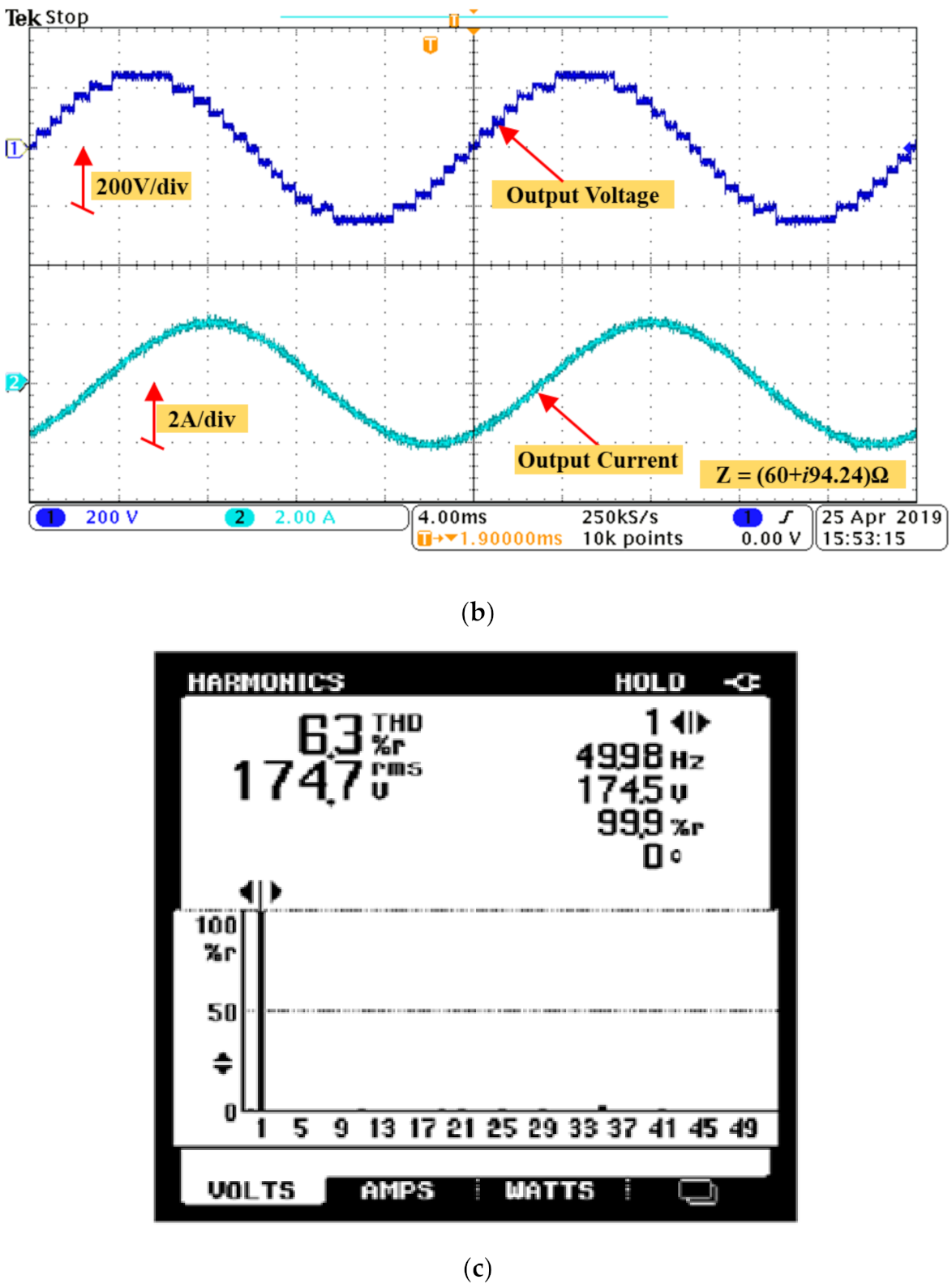
3. Simulation and Experimental Results

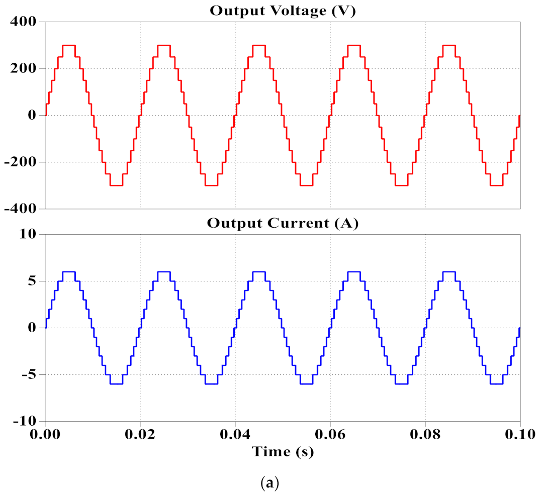
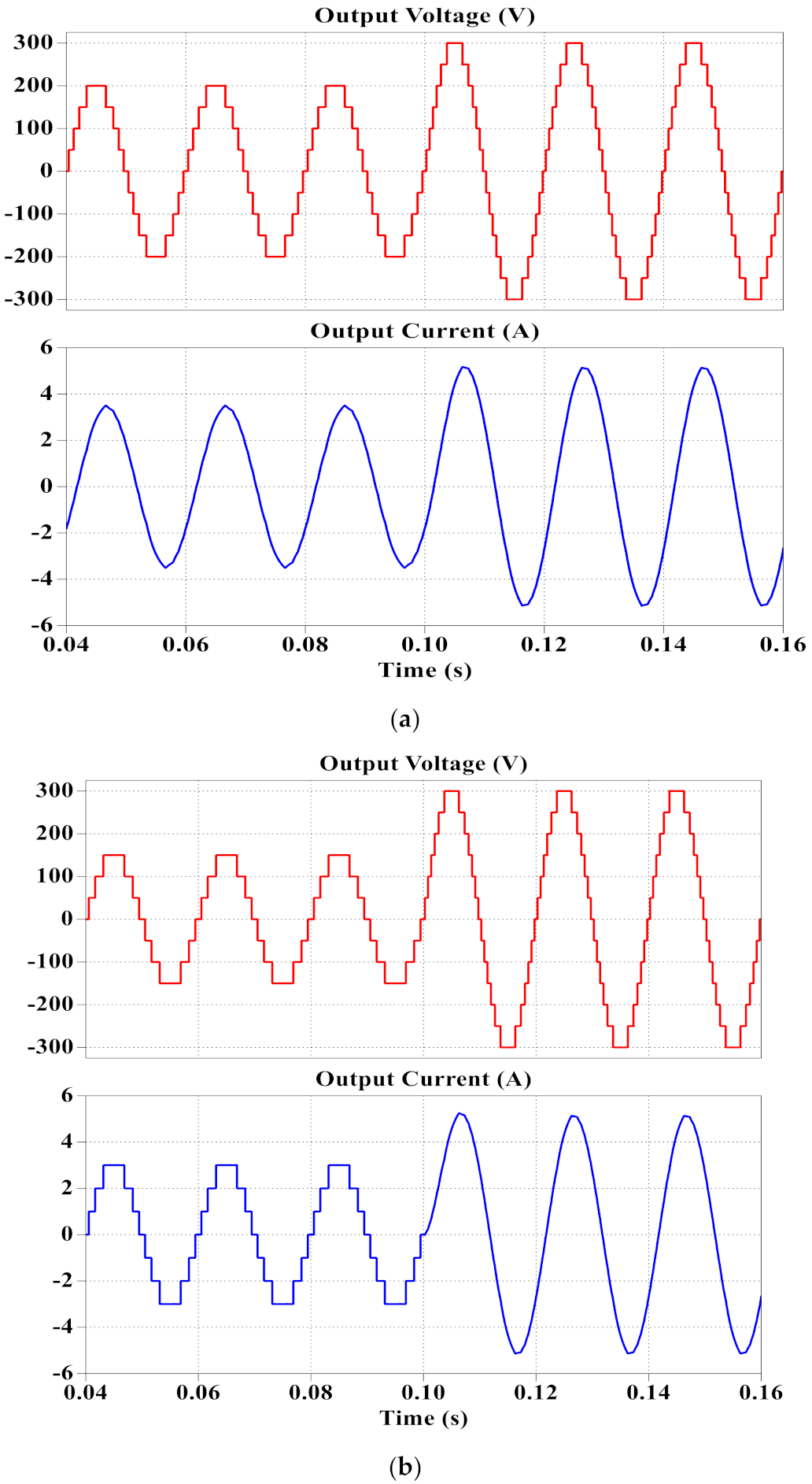
3.1. Simulation Results

To verify the performance of the proposed topology, a simulation is carried out using the PLECS software. The magnitude of voltage sources is selected as V1 = 50 V, V2 = 100 V, and V11 = 150 V. Initially the inverter is made to feed a resistive load of 50 Ω. With the size of each step as 50 V, the peak voltage obtained at the inverter terminals is 300 V with six steps. A corresponding load current with a peak magnitude of 6A is observed at the load as shown in Figure 7a. When the topology was made to feed an R-L load 50 Ω and 100 mH, the load current is obtained as 5.07 A, with the load impedance being 50 + j31.41 Ω. The inductive reactance of the load naturally filters the current waveform. Therefore, the load current observed in the inductive load appears to be a smoother sine wave as shown in Figure 7b when compared to its resistive load counterpart.
To analyze the dynamic response of the system the modulation index is subjected to a sudden change and the response of the system is observed. With an R-L load of 50 Ω and 100 mH, the voltage and current transition is smooth while the modulation index is changed at 0.10 s as shown in Figure 8a. Further, the number of levels obtained at the modulation index of 1.0 is six when compared to four at a modulation index of 0.67. The topology is also subjected to a simultaneous change in load from R to R-L and a change in modulation index from 0.50 to 1.0 as shown in Figure 8b. In that case, the load current is observed to be smoothened at 0.10 s since the inductive load is a natural filter. The three positive and negative levels lost at a modulation of the index of 0.5 is regained at 0.1 s. Thus, validating the seamless performance of the topology under dynamic conditions.

3.2. Experimental Results

In order to verify the simulation results, a hardware prototype is built. TOSHIBA IBGT GT50J325 is used as a switching device. dSPACE CP1104 is used to generate the gate pulses and is made suitable for switches via the gate driver circuit. The hardware prototype developed is shown in Figure 9. For the experimental results. The magnitude of dc voltage sources is selected as V1 = 40 V, V2 = 80 V, and V11 = 120 V.
Figure 10a shows the experimental results with output voltage and current waveforms with a resistive load. For a peak load voltage of 240 V, the peak current is observed as 4A at a load of 60 Ohm as shown in Figure 10a. When the load is changed to 60 ohms with an inductance of 300 mH to form the existing R-Load, the peak load current is obtained as 2A and it has got smoother as shown in Figure 10b. In both cases, a modulation index (MI) of 1.0 is used. Figure 10c shows the harmonic spectrum of output voltage and the THD comes out to be 6.3%.
When the experimental prototype is subjected to a sudden change in modulation index, that is if the modulation index is lowered to 0.4 from 1.0, the peak voltage reduces to 100 V, and the load current is observed as 1.3A as shown in Figure 11a. Similarly, for the R-Load of 60 ohms and an inductance of 300 mH, the inverter has undergone a smooth switchover and the load voltage and current waveform obtained are shown in Figure 11b as MI is changed from 1.0 to 0.4.
Further, when the topology is subjected to the sudden load addition from no load to a load of 60 ohm and 300 mH, the current waveform undergoes a smooth transition with zero overshoot as shown in Figure 12a. Figure 12b shows the response of the inverter for a consequent disturbance of change in load with a modulation index of 1.0. Firstly, the load terminals are open, which results in zero load current. After few cycles of the output voltage, a load of 120 ohm is connected across the load terminals, which draws a current of 2A, peak, and after few cycles of the output voltage, another resistance of 120 ohm is connected in parallel to the existing 120 ohm. Thus, the effective load resistance becomes 60ohm, hence a peak load current of 4A is drawn from the inverter. From Figure 12b, it can be observed that both the disturbances are taken seamlessly by the inverter. From all these simulations and experimental results, it can be concluded that the performance of the proposed topology is satisfactory steady as well as dynamic loading conditions. The dynamic load test is essential for the application of the proposed topology for electrical drive application. The results with a change of load, change of modulation index, doubling of load current confirm the satisfactory performance of the proposed topology under dynamic loading conditions.

4. Conclusions

A new hybrid MLI topology is proposed in this paper with a reduced number of switches and dc voltage sources. The proposed topology is able to produce a higher number of levels at the output by connecting several auxiliary units to the proposed basic unit. The efficiency of the topology is estimated as 98.5%. From the components and cost comparison made, it has been observed that the number of components required for building the topology is less when compared to the topologies proposed in recent literature and consequently the cost of the topology is less. For the proposed 13 levels, a THD of 6.3% has been obtained with the NLCPWM. The performance of the topology is validated with simulation and experimental results. A 500 W low power laboratory prototype has been used for the validation of the proposed topology and different loading conditions have been tested. The loading conditions used for the validation of the proposed topology include fixed as well as dynamic load. Change of load, change of modulation index, and doubling of load current has been validated with the proposed topology. One of the major limitations of the proposed topology has been the use of an H-bridge. Another limitation has been the requirement of a higher number of isolated sources. Further research related to the proposed topology will be the reduction in the voltage stress of H-bridge switches with improved modulation techniques. Further, the application of solar PV panels with the proposed topology will be another future task. Modulation index has an important role in the performance improvements like improved power loss with the better harmonic profile of the output voltage and current. Therefore, an improved modulation technique needs to be developed and tested with the proposed topology.

Author Contributions

Conceptualization, M.R., P.P., J.S.M.A. and S.M.; methodology, M.R., P.P., J.S.M.A. and S.M.; validation, M.R., M.D.S. and S.M.; formal analysis, P.P., A.W., M.D.S., M.S. and S.M.; investigation, A.W., M.D.S., M.S. and A.S.; writing—original draft preparation, P.P., J.S.M.A., A.W., M.R., M.S. and A.S.; writing—review and editing, P.P., J.S.M.A., A.W., M.R., M.S. and A.S.; supervision, S.M., A.W., M.D.S., M.S. and A.S.; funding acquisition, S.M., A.W., M.R., M.S. and A.S. All authors have read and agreed to the published version of the manuscript.

Funding

This work was supported by the Asian University Alliance (AUA)-UAE-U under Grant 12R022.

Institutional Review Board Statement

Not applicable.

Informed Consent Statement

Not applicable.

Data Availability Statement

Not applicable.

Conflicts of Interest

The authors declare no conflict of interest.

References

  1. Bughneda, A.; Salem, M.; Richelli, A.; Ishak, D.; Alatai, S. Review of multilevel inverters for PV energy system applications. Energies 2021, 14, 1585. [Google Scholar] [CrossRef]
  2. Zhang, J.; Xu, S.; Din, Z.; Hu, X. Hybrid Multilevel Converters: Topologies, Evolutions and Verifications. Energies 2019, 2, 615. [Google Scholar] [CrossRef] [Green Version]
  3. Xue, Q.; Zhang, X.; Teng, T.; Zhang, J.; Feng, Z.; Lv, Q. A Comprehensive Review on Classification, Energy Management Strategy, and Control Algorithm for Hybrid Electric Vehicles. Energies 2020, 13, 5355. [Google Scholar] [CrossRef]
  4. di Benedetto, M.; Lidozzi, A.; Solero, L.; Crescimbini, F.; Grbović, P.J. High-performance 3-phase 5-level e-type multilevel–multicell converters for microgrids. Energies 2021, 14, 843. [Google Scholar] [CrossRef]
  5. Majstorovic, M.; Rivera, M.; Ristic, L.; Wheeler, P. Comparative study of classical and mpc control for single-phase mmc based on v-hil simulations. Energies 2021, 14, 3230. [Google Scholar] [CrossRef]
  6. Espinosa, E.; Melín, P.; Baier, C.; Espinoza, J.; Garcés, H. An Efficiency Analysis of 27 Level Single-Phase Asymmetric Inverter without Regeneration. Energies 2021, 14, 1459. [Google Scholar] [CrossRef]
  7. Loganathan, V.; Srinivasan, G.K.; Rivera, M. Realization of 485 level inverter using tri-state architecture for renewable energy systems. Energies 2020, 13, 6627. [Google Scholar] [CrossRef]
  8. Anand, V.; Singh, V. Compact symmetrical and asymmetrical multilevel inverter with reduced switches. Int. Trans. Electr. Energy Syst. 2020, 30, e12458. [Google Scholar] [CrossRef]
  9. Anand, V.; Singh, V. Implementation of cascaded asymmetrical multilevel inverter for renewable energy integration. Int. J. Circuit Theory Appl. 2020, 2944. [Google Scholar] [CrossRef]
  10. Babaei, E.; Alilu, S.; Laali, S. A new general topology for cascaded multilevel inverters with reduced number of components based on developed H-bridge. IEEE Trans. Ind. Electron. 2014, 61, 3932–3939. [Google Scholar] [CrossRef]
  11. Alishah, R.S.; Nazarpour, D.; Hosseini, S.H.; Sabahi, M. Reduction of power electronic elements in multilevel converters using a new cascade structure. IEEE Trans. Ind. Electron. 2015, 62, 256–259. [Google Scholar] [CrossRef]
  12. Gupta, K.K.; Jain, S. Comprehensive review of a recently proposed multilevel inverter. IET Power Electron. 2014, 7, 467–479. [Google Scholar] [CrossRef]
  13. Prem, P.; Bharanikumar, R. Design and mathematical evaluation of a new multilevel inverter topology with less circuit components for solar and wind energy conversion systems. Appl. Math. Inf. Sci. 2017, 11, 1115–1122. [Google Scholar] [CrossRef]
  14. Siddique, M.D.; Mekhilef, S.; Shah, N.M.; Memon, M.A. Optimal Design of a New Cascaded Multilevel Inverter Topology with Reduced Switch Count. IEEE Access 2019, 7, 24498–24510. [Google Scholar] [CrossRef]
  15. Masaoud, A.; Mekhilef, S.; Ping, H.W.; Wong, K.I. A simplified structure for three-phase 4-level inverter employing fundamental frequency switching technique. IET Power Electron. 2017, 10, 1870–1877. [Google Scholar] [CrossRef]
  16. Samadaei, E.; Gholamian, S.A.; Sheikholeslami, A.; Adabi, J. An Envelope Type (E-Type) Module: Asymmetric Multilevel Inverters with Reduced Components. IEEE Trans. Ind. Electron. 2016, 63, 7148–7156. [Google Scholar] [CrossRef]
  17. Gautam, S.P.; Sahu, L.K.; Gupta, S. Reduction in number of devices for symmetrical and asymmetrical multilevel inverters. IET Power Electron. 2016, 9, 698–709. [Google Scholar] [CrossRef]
  18. Jayabalan, M.; Jeevarathinam, B.; Sandirasegarane, T. Reduced switch count pulse width modulated multilevel inverter. IET Power Electron. 2017, 10, 10–17. [Google Scholar] [CrossRef]
  19. Samadaei, E.; Sheikholeslami, A.; Gholamian, S.A.; Adabi, J. A Square T-Type (ST-Type) Module for Asymmetrical Multilevel Inverters. IEEE Trans. Power Electron. 2018, 33, 987–996. [Google Scholar] [CrossRef]
  20. Prem, P.; Sathik, J.; Sivaraman, P.; Mathewsaran, A.; Aleem, S.H.E.A. A new asymmetric dual source multilevel inverter topology with reduced power switches. J. Chin. Inst. Eng. Trans. Chin. Inst. Eng. A 2019, 42, 460–472. [Google Scholar] [CrossRef]
  21. Prem, P.; Sugavanam, V.; Abubakar, A.I.; Ali, J.S.M.; Sengodan, B.C.; Krishnasamy, V.; Padmanaban, S. A novel cross-connected multilevel inverter topology for higher number of voltage levels with reduced switch count. Int. Trans. Electr. Energy Syst. 2020, 30, e12381. [Google Scholar] [CrossRef]
  22. Ali, J.S.M.; Kannan, R. A new symmetric cascaded multilevel inverter topology using single and double source unit. J. Power Electron. 2015, 15, 951–963. [Google Scholar] [CrossRef] [Green Version]
  23. Ramani, K.; Sathik, M.A.J.; Sivakumar, S. A new symmetric multilevel inverter topology using single and double source sub-multilevel inverters. J. Power Electron. 2015, 15, 96–105. [Google Scholar] [CrossRef] [Green Version]
  24. Alishah, R.S.; Hosseini, S.H.; Babaei, E.; Sabahi, M. A New General Multilevel Converter Topology Based on Cascaded Connection of Submultilevel Units with Reduced Switching Components, DC Sources, and Blocked Voltage by Switches. IEEE Trans. Ind. Electron. 2016, 63, 7157–7164. [Google Scholar] [CrossRef]
  25. Buccella, C.; Cecati, C.; Cimoroni, M.G.; Razi, K. Analytical method for pattern generation in five-level cascaded H-bridge inverter using selective harmonic elimination. IEEE Trans. Ind. Electron. 2014, 61, 5811–5819. [Google Scholar] [CrossRef]
  26. Alishah, R.; Nazarpour, D.; Hosseini, S.H.; Sabahi, M. Novel topologies for symmetric, asymmetric, and cascade switched-diode multilevel converter with minimum number of power electronic components. IEEE Trans. Ind. Electron. 2014, 61, 5300–5310. [Google Scholar] [CrossRef]
  27. Neti, S.S.; Anand, V.; Singh, V. Single-Phase Generalized Switched-Capacitor Multilevel Inverter Using Reduced Number of Power Semiconductor Components with Voltage Boosting Ability. Arab J. Sci. Eng. 2021. [Google Scholar] [CrossRef]
  28. Babaei, E.; Laali, S.; Bayat, Z. A single-phase cascaded multilevel inverter based on a new basic unit with reduced number of power switches. IEEE Trans. Ind. Electron. 2015, 62, 922–929. [Google Scholar] [CrossRef]
  29. Siddique, M.D.; Ali, J.S.M.; Mekhilef, S.; Mustafa, A.; Sandeep, N.; Almakhles, D. Reduced Switch Count Based Single Source 7L Boost Inverter Topology. IEEE Trans. Circuits Syst. Express Briefs 2020, 67, 3252–3256. [Google Scholar] [CrossRef]
  30. Siddique, M.D.; Mekhilef, S.; Mekhilef, S.; Shah, N.M.; Ali, J.S.M.; Blaabjerg, F. A new switched capacitor 7L inverter with triple voltage gain and low voltage stress. IEEE Trans. Circuits Syst. Express Briefs 2020, 67, 1294–1298. [Google Scholar] [CrossRef]
  31. Siddique, M.D.; Mekhilef, S.; Padmanaban, S.; Memon, M.A.; Kumar, C. Single Phase Step-up Switched-Capacitor Based Multilevel Inverter Topology with SHEPWM. IEEE Trans. Ind. Appl. 2021, 57, 3107–3119. [Google Scholar] [CrossRef]
  32. Camurca, L.; Langwasser, M.; Liserre, M. Design Approach of Inductive Components in Medium Voltage Modular Multilevel Converter Considering DC Side Fault Protection Conditions. In Proceedings of the IEEE Applied Power Electronics Conference and Exposition—PEC, Virtual Conference, 14–17 June 2021; pp. 2617–2624. [Google Scholar] [CrossRef]
  33. Marquez, A.; Monopoli, V.G.; Tcai, A.; Leon, J.I.; Buticchi, G.; Vazquez, S.; Liserre, M.; Franquelo, L.G. Discontinuous-PWM Method for Multilevel N-Cell Cascaded H-Bridge Converters. IEEE Trans. Ind. Electron. 2020, 68, 7996–8005. [Google Scholar] [CrossRef]
Figure 1. Proposed hybrid inverter topology.
Energies 14 04709 g001
Figure 2. Different switching states of level generation unit (a) Vo = V1, (b) Vo = V2, (c) Vo = V1 + V2, (d) Vo = V11 + V1, (e) Vo = V11 + V2, and (f) Vo= V11 + V1 + V2.
Energies 14 04709 g002
Figure 3. Generalized structure of the proposed topology.
Energies 14 04709 g003
Figure 4. NLCPWM with (a) Synthesizing the Terminal Voltage from Reference (b) Switching Function of NLM method.
Energies 14 04709 g004
Figure 5. Efficiency plot of the proposed topology.
Energies 14 04709 g005
Figure 6. Optimization of structures for maximizing the number of levels for constant (a) number of switches (b) number of drivers and (c) number of dc sources.
Energies 14 04709 g006
Figure 7. Simulation results (a) Terminal voltage and Load current for R load. (b) Terminal voltage and Load current for R-L load.
Energies 14 04709 g007aEnergies 14 04709 g007b
Figure 8. Terminal voltage and Load current for (a) change of MI with R-L load and (b) change of MI and load from R load to R-L load.
Energies 14 04709 g008
Figure 9. Experimental Prototype.
Energies 14 04709 g009
Figure 10. Terminal voltage and Load current for (a) R load and (b) R-L load, and (c) harmonic spectrum of output voltage.
Energies 14 04709 g010aEnergies 14 04709 g010b
Figure 11. Terminal voltage and Load current with a change of MI with (a) R load and (b) R-L load.
Energies 14 04709 g011
Figure 12. Terminal voltage and Load current for dynamic change in load with a change of load from (a) no-load to 60 ohm + 300 mH and (b) no-load to 120 ohm to 60 ohm.
Energies 14 04709 g012
Table 1. Switching Table.
S1S2S3S11S12S21S22---Sm1Sm2H1H2H3H4Load Voltage (V)
0010101--011010V1
1000101--011010V2
0100101--011010V1 + V2
0011001--011010V11 + V1
1001001--011010V11 + V2
0101001--011010V11 + V1+ V2
0011010-011010V21 + V11 + V1
1001010--011010V21 + V11 + V2
0101010--011010V21 + V11 + V1+ V1
---------------------------------------------
0011010--101010Vm1 + V21 + V11 + V1
1001010--101010Vm1 + V21 + V11 + V2
0101010--101010Vm1 + V21 + V11 + V1 + V1
0010101--010101−V1
1000101--010101−V2
0100101--010101−(V1 + V2)
0011001--010101−(V11 + V1)
1001001--010101−(V11 + V2)
0101001--010101−(V11 + V1+ V2)
0011010-010101−(V21 + V11 + V1)
1001010--010101−(V21 + V11 + V2)
0101010--010101−(V21 + V11 + V1+ V1)
---------------------------------------------
0011010--100101−(Vm1 + V21 + V11 + V1)
1001010--100101−(Vm1 + V21 + V11 + V2)
0101010--100101−(Vm1 + V21 + V11 + V1 + V1)
Table 2. Components and Cost Comparison.
S.NoParameter[13][20][21][19][17][18][24][28]Proposed
1Number of independent sources624424673
2Number of capacitors-4--3----
3Number of IGBTs1091412810161610
4Number of drivers8713981012147
5Number of diodes1---14----
6Cost of IGBT in USD (at 1 USD per IGBT)109149810161610
7Cost of Driver in USD (at 5.25 USD per IGBT)4236.7568.2547.254252.56373.536.75
8Cost of diodes in USD (at 3.63 USD per diode)3.63---50.82----
9Cost of capacitor in USD (at 1.82 USD per capacitor)-7.28--5.46----
10Total cost (USD)80.6375.03113.2581.2141.2886.5113126.566.75
11Experimental output power (W)3245017024064300570125500
Publisher’s Note: MDPI stays neutral with regard to jurisdictional claims in published maps and institutional affiliations.

