Article

Circuit Structure and Control Method to Reduce Size and Harmonic Distortion of Interleaved Dual Buck Inverter

Department of Electrical engineering, Pohang University of science and technology, Pohang 790-783, Korea
*
Author to whom correspondence should be addressed.
Energies 2020, 13(6), 1531; https://doi.org/10.3390/en13061531
Submission received: 13 January 2020 / Revised: 12 March 2020 / Accepted: 19 March 2020 / Published: 24 March 2020
(This article belongs to the Section F: Electrical Engineering)

Abstract

:
A new circuit structure and control method for a high power interleaved dual-buck inverter are proposed. The proposed inverter consists of six switches, four diodes and two inductors, uses a dual-buck structure to eliminate zero-cross distortion, and operates in an interleaved mode to reduce the current stress of switch. To reduce the total harmonic distortion at low output power, the inverter is controlled using discontinuous-current-mode control combined with continuous-current-mode control. The experimental inverter had a power-conversion efficiency of 98.5% at output power = 1300 W and 98.3% at output power = 2 kW, when the inverter was operated at an input voltage of 400 VDC, output voltage of 220 VAC/60 Hz, and switching frequency of 20 kHz. The total harmonic distortion was < 0.66%, which demonstrates that the inverter is suitable for high-power dc-ac power conversion.

1. Introduction

The full-bridge inverter (FBI, Figure 1a) is widely used for dc-ac power conversion because of its simple structure and easy control [1]. An FBI uses sinusoidal modulation of the switching duty to produce an alternating output voltage. The FBI has a shoot-through problem [2], which occurs when the high side and low side switches (S1 and S4, or S3 and S2) are turned on at the same time; this problem can cause serious circuit damage. The shoot-through problem can be solved by inserting a dead-time between the gate pulses of the high and low side switches, but inserting a dead-time changes the effective switching duty ratio and increases zero-cross distortion (ZCD) [3]. The FBI has the other disadvantage of requiring high-rated switches and large output filters [4,5].
Various dual-buck inverters [6,7,8,9,10,11,12,13,14,15] have been proposed to remedy the disadvantages of the FBI. The dual-buck inverters use freewheeling diodes to solve the shoot-through problem but have high output current ripple. The interleaved dual-buck inverter (IDBI) in [9], as shown in Figure 1b, is basically a parallel connection of four buck converters. In this inverter, SU1 and SU2 operate to generate positive sinusoidal voltage, SD1 and SD2 operate to generate negative sinusoidal voltage, and the switching-phase differences between SU1 and SU2 and between SD1 and SD2 are set to 180°. Thus, the current of SU1 is interleaved with that of SU2, and the current of SD1 is interleaved with that of SD2. Using an interleaved mode reduces conduction losses, output current ripple, and current stress in switches and diodes. IDBI requires four inductors, so it is expensive and bulky. When IDBI uses typical sinusoidal pulse width control and operates at a low output power Po, IDBI has much higher total harmonic distortion (THD) of the output current than that of the FBI.
The inverter proposed in this paper (Figure 2) is a modified IDBI. This inverter inherits the IDBI’s advantages but uses two reverse-current-protection diodes DD3 and DU3 to reduce the number of inductors and a new control method to reduce the THD of the output current. The proposed inverter operates in discontinuous conduction mode (DCM) [16] when the output current is below the threshold; otherwise, it operates in continuous conduction mode (CCM). The circuit structure and principle of operation are described in Section 2, experimental results and discussions are given in Section 3, and a conclusion is given in Section 4.

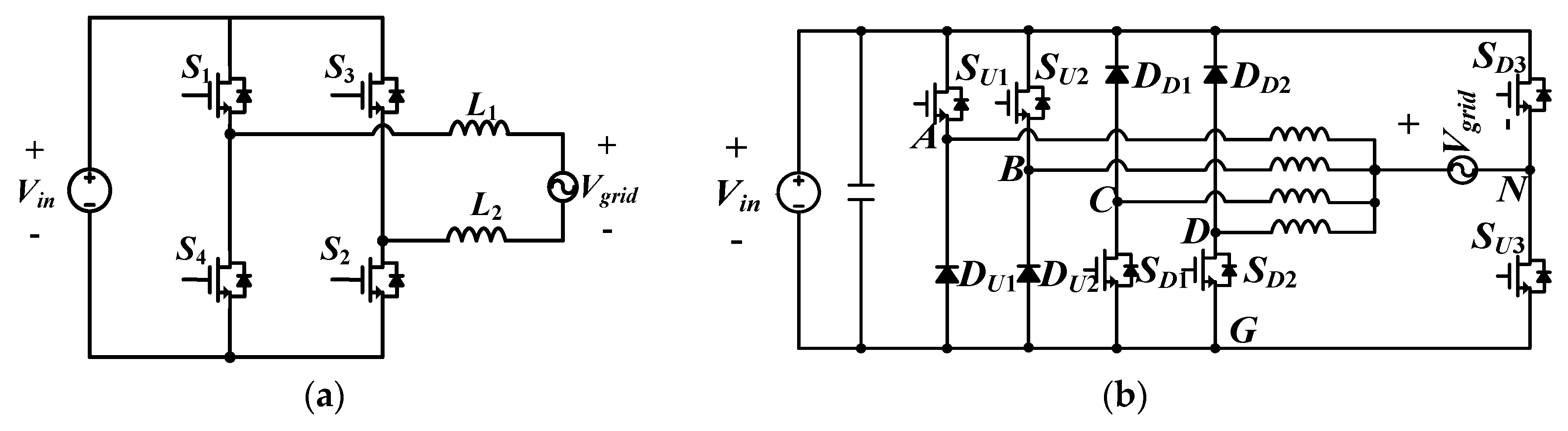
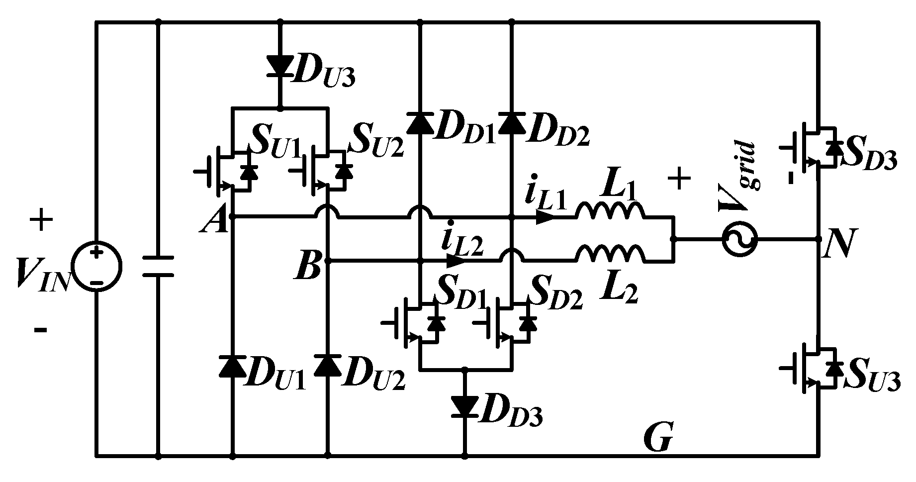
2. Proposed Interleaved Dual-buck Inverter

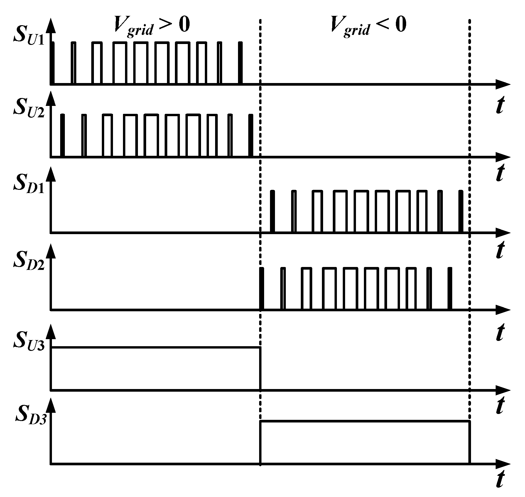
2.1. Circuit Structure and Principle of Operation

The proposed inverter (Figure 2) uses two dual-buck legs (leg 1: SU1, DU1; leg 2: SU2, DU2) to generate Vgrid ≥ 0 V, two dual-buck legs (leg 3: SD1, DD1; leg 4: SD2, DD2) to generate Vgrid < 0 V, two blocking diodes (DU3, DD3) to prevent the current flowing through the body diode of switch during freewheeling mode, and two unfolding switches (SU3, SD3) to determine the polarity of the output current. Legs 1 and 4 are connected to L1, and legs 2 and 3 are connected to L2. Therefore, the proposed inverter requires two inductors, unlike interleaved dual-buck inverters, which have four legs and one inductor per leg. The proposed inverter works with the switching states and leg voltages VAN_on and VAN_off in Table 1. Leg switches SU1, SU2, SD1, and SD2 operate at a fixed switching frequency fs = 1/Ts, where Ts is the switching period. The switching duty D is varied to produce a sinusoidal output voltage V g r i d ( t ) = V g sin ( ω t ) .
The simplified gate signals (Figure 3) for the proposed inverter show that legs 1 and 2 operate for Vgrid > 0 V and legs 3 and 4 operate for Vgrid < 0 V. SU3 turns for Vgrid ≥ 0 V and SD3 turns on for Vgrid < 0 V. To obtain interleaved dual-buck operation, the switching phase differences between SU1 and SU2 and between SD1 and SD2 are set to Ts/2. The difference in switching phases reduces ZCD and prevents shoot-through without inserting dead time between switching pulses (Table 1).
When Vgrid > 0 V, the current iL1 and voltage VL1 waveforms of the inductor L1 (Figure 4a) consist of three operating modes: Mode 1 during which the input energy is delivered to L1 and the load; Mode 2 during which the stored energy in L1 is delivered to the load; and Mode 3 during which the stored energy in L1 = 0; Mode 3 occurs only when the inverter operates in DCM.
Mode 1 starts at t 0 = ( n 1 ) T s by turning on SU1 (Figure 4b), where the integer n is a switching sequence number. During this mode, the output voltage V A N of leg 1 is V i n . The inductor current i L 1 ( t ) increases as t increases, because V L 1 = V A N V g r i d > 0 V and
i L 1 ( t ) = i L 1 ( t 0 ) + 1 L 1 t 0 t V L 1 ( t ) d t .
Mode 2 starts at t 1 = ( n 1 + D ) T s by turning off SU1 (Figure 4c). During this mode, V A N is 0 V. i L 1 ( t ) decreases as t increases because V L 1 = V A N V g r i d < 0 V and
i L 1 ( t ) = i L 1 ( t 1 ) + 1 L 1 t 1 t V L 1 ( t ) d t .
Mode 3 starts at t 2 = ( n 1 + Δ ) T s where Δ T s is duration of i L 1 ( t ) > 0 , when DU1 is turned off (Figure 4d). This mode is skipped when Δ = 1 , i.e., when the inverter is operating in CCM. During this mode, V A N = V g r i d because i L 1 ( t ) = 0 and the energy stored in L1 is 0.
The voltage V A N of node A with respect to node N equals to V g r i d + V L 1 ( t ) . The switching states (Table 1) produce V A N = V i n in Mode 1, V A N = 0 V in Mode 2, and V A N = V g r i d in Mode 3. The average of V A N for one switching period is expressed as
V A N _ a v g = V g r i d + V L 1 _ a v g = V g r i d + L 1 d i L 1 _ a v g d t .
SU1 operates with a switching duty of D = DSU1. V A N _ a v g can also be expressed as
V A N _ a v g = V i n D S U 1 + V g r i d ( 1 Δ ) ,
because VAN = Vin in Mode 1, VAN = 0 V in Mode 2, and VAN = Vgrid in Mode 3. Solving for Δ using (3) and (4) yields
Δ = V i n D S U 1 V g r i d L 1 V g r i d d i L 1 _ a v g d t .
i L 1 _ a v g is calculated using Equations (1) and (2) as
i L 1 _ a v g i L 1 ( t 0 ) + ( V i n V g r i d ( t 0 ) 2 L 1 ) D S U 1 T s Δ .
To achieve a power factor of 1, the time average of output current i o _ a v g should be I o sin ( ω t ) for V g r i d ( t ) = V g sin ( ω t ) . The inverter has L 1 = L 2 = L and operates in interleaved dual-buck mode, so i o _ a v g = 2 i L 1 _ a v g . When the inverter operates in DCM, D S U 1 at t = t 0 to produce sinusoidal i o _ a v g is obtained using Equations (5) and (6), 2 π f s > > ω and i L 1 ( t 0 ) = 0 as
D S U 1 = L I o V g sin 2 ( ω t ) V i n ( V i n 2 V g sin ( ω t ) ) T s + ( ω L I o cos ( ω t ) 4 V i n ) 2 + ω L I o cos ( ω t ) 4 V i n .
When the inverter is operating in CCM, Δ = 1 and D S U 1 at t = t 0 is obtained using Equation (5) as
D S U 1 = V g sin ( ω t ) V i n + ω L I o cos ( ω t ) 2 V i n .
The DCM interval during which the inverter operates in DCM is calculated using Equations (5), (7), and Δ 1 as
0 < ω t sin 1 ( V i n V g ( 1 L I o V g T s ) )
when Vgrid increases, and
π sin 1 ( V i n V g ( 1 L I o V g T s ) ) ω t < π ,
when Vgrid decreases.
The condition for operating the inverter only in CCM is obtained by setting the argument of arcsine in Equations (9) and (10) less than 0, and is given as
I o > V g T s L ,
and the condition for operating the inverter only in DCM is obtained by setting the argument of arcsine in Equations (9) and (10) greater than 1, and is given as
I o < V g T s L ( 1 V g V i n ) .
The waveforms iL2 and VL2 of the inductor L2 for Vgrid > 0 V are the same as iL1 and VL1 except that they are delayed by Ts/2.
The waveforms iL1, VL1, iL2, and VL2 for Vgrid < 0 V are identical to the waveforms iL2, VL2, iL1, and VL1 for Vgrid > 0 V, respectively, except that the polarity is reversed.

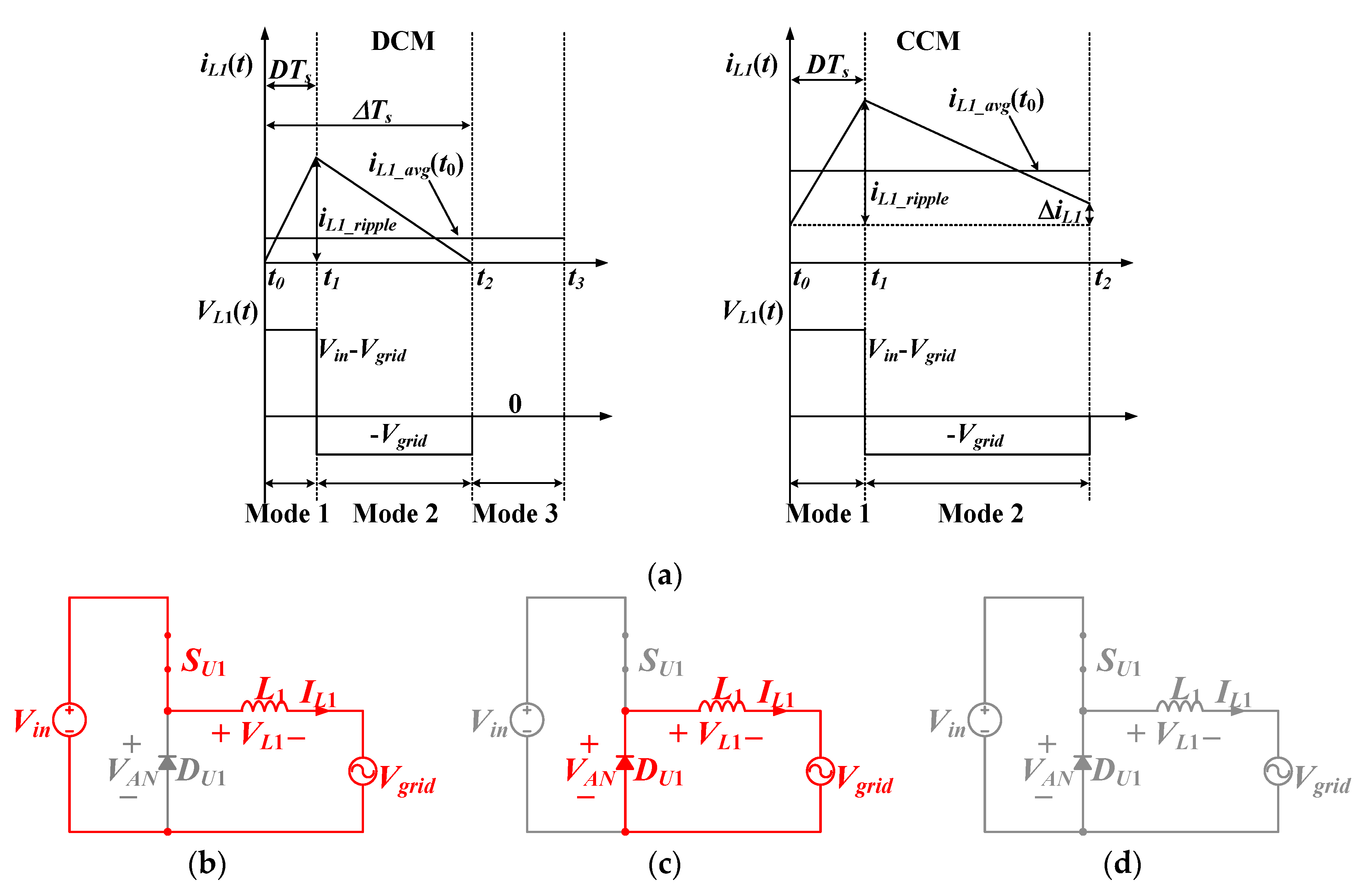
2.2. Design Constraint for L1 and L2

The inverter must operate at I o I o , max . The highest switching duty D S U 1 _ max of SU1 is calculated using Equation (8) as
D S U 1 _ max = 4 V g 2 + ( ω L I o _ max ) 2 2 V i n < 1
which results in the upper bound of L 1 = L 2 = L as
L < 2 V i n 2 V g 2 ω I o _ max .
This condition gives L < 103.44 mH when P o = 2 kW and I o _ max = 12.9 A.
The current and voltage waveforms for L 2 are same as those for L 1 , except the time delay by T s / 2 ; hence, the output current ripple i o _ r i p p l e of the proposed inverter can be calculated using Equations (1), (2) and (8) as
i o _ r i p p l e = V i n T s L D ( 1 2 D ) .
for 0 < D < 1/2 and
i o _ r i p p l e = V i n T s L ( 1 D ) ( 2 D 1 ) .
for 1/2 < D < 1; the highest i o _ r i p p l e occurs at D = 1/4 or 3/4. After allowing the highest i o _ r i p p l e of 1 A at Po = 2 kW and f s = 20 kHz (this condition corresponds to THD < 3%), the lower bound of L is obtained using Equations (15) and (16) as
L V i n T s 8 i o _ r i p p l e _ max 2.5   mH .
L min = 2.5 mH was used in the experimental inverters to minimize the inductor size.

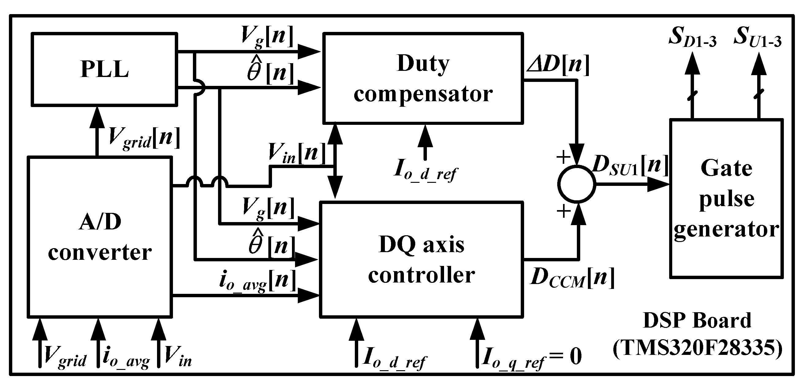
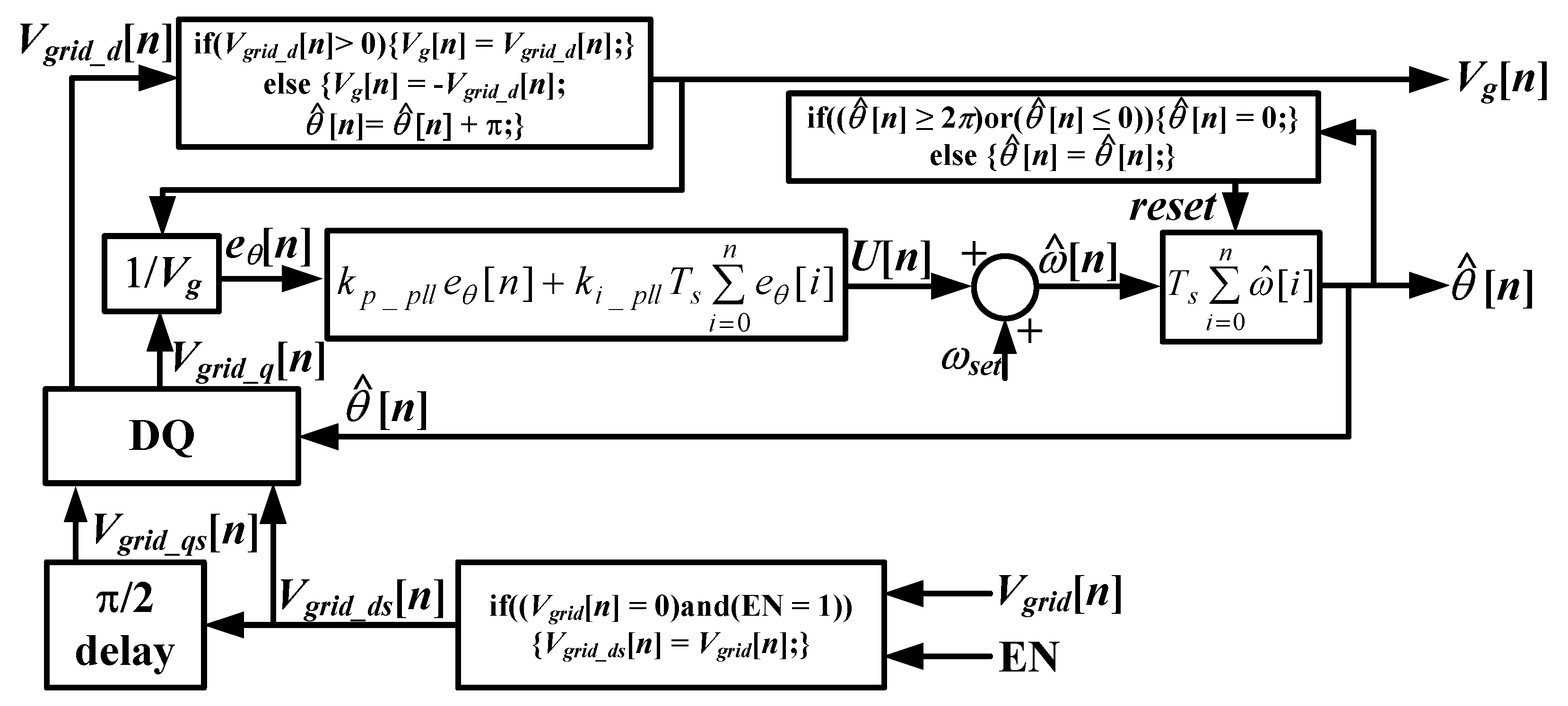
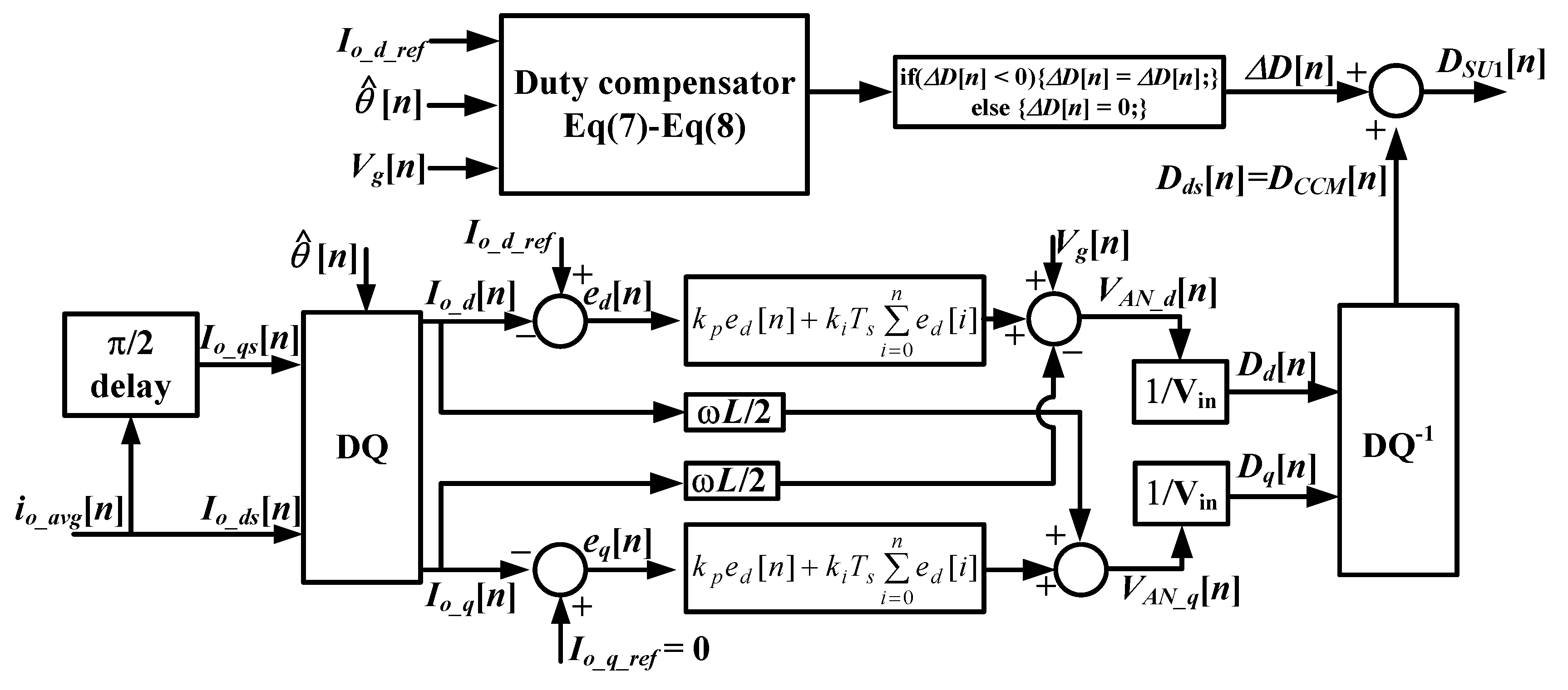
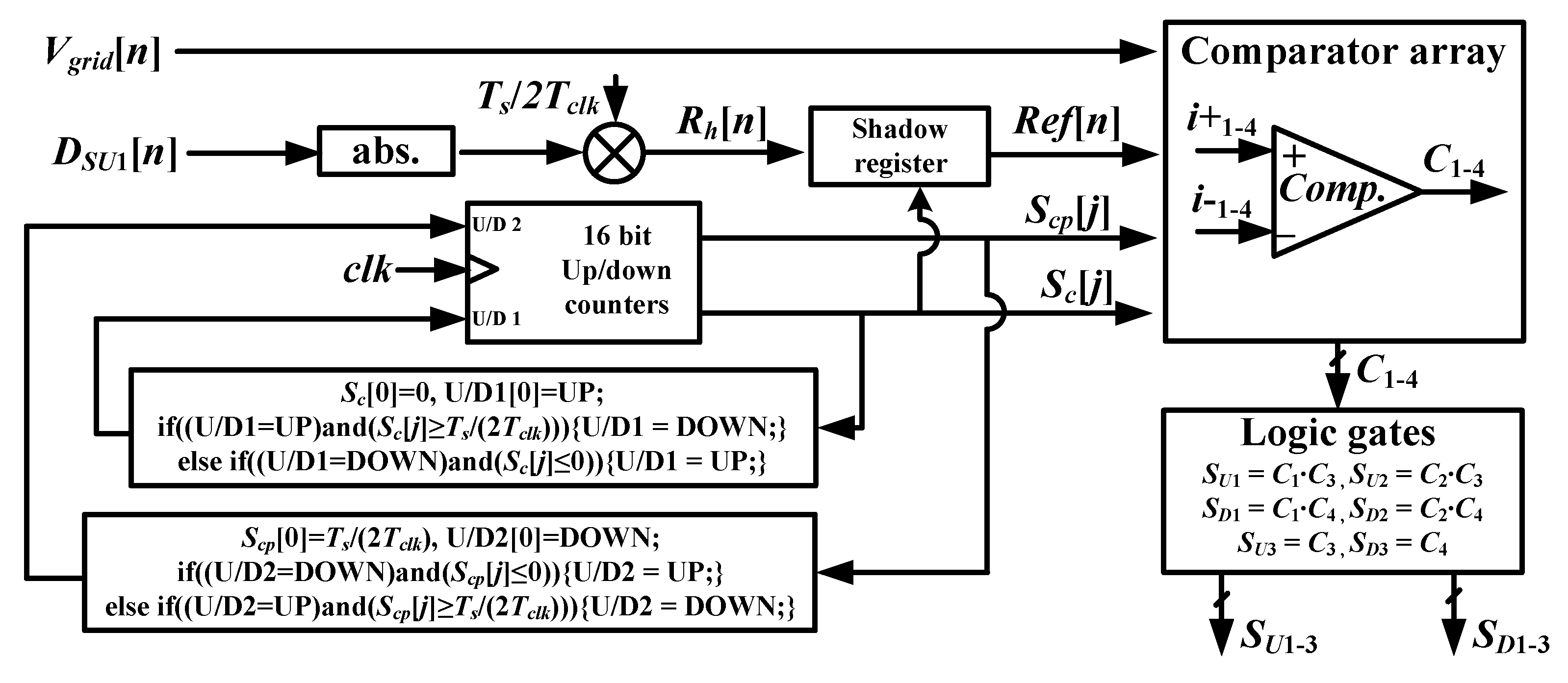
2.3. Controller Design

The controller (Figure 5) was designed using Texas Instrument’s TMS320F28335 digital signal processor (DSP). This controller inputs Vgrid, io_avg, and Vin and uses the D-Q axis control method [17] to produce gating signals SU1SU3 and SD1SD3 that can generate a sinusoidal io_avg. The controller consists of a phase-locked loop (PLL), a D-Q axis controller, and a gate pulse generator. The DSP operates at a clock frequency fclk = 1/Tclk = 150 MHz and the sampling frequency is the same as the switching frequency fs = 1/Ts = 20 kHz. Thus, the sampling sequence number n is in the range of 0 ≤ n ≤ 332 when the grid frequency f = ω/2π = 60 Hz, and clock sequence number j is in the range of 0 ≤ j ≤ 7499.
The PLL (Figure 6) sets n = 0 and starts to operate when Vgrid = 0 and the enable signal EN = 1. This circuit inputs Vgrid and estimates the amplitude Vg and phase θ ^ = ω ^ t of Vgrid. Using V g r i d [ n ] = V g sin ( θ [ n ] ) , the PLL generates a virtual grid-voltage Vgrid_qs as
V g r i d _ q s [ n ] = V g cos ( θ [ n ] )
θ ^ [ 0 ] has been set to 0 if Vgrid_qs [0] ≥ 0 and to π otherwise. Thus, the initial estimation error e θ [ 0 ] = θ [ 0 ] θ ^ [ 0 ] is very small. Vgrid and Vgrid_qs are transformed into the voltages Vgrid_d and Vgrid_q in the synchronous reference frame as
( V g r i d _ d V g r i d _ q ) = ( sin ( θ ^ [ n ] ) cos ( θ ^ [ n ] ) cos ( θ ^ [ n ] ) sin ( θ ^ [ n ] ) ) ( V g r i d _ d s V g r i d _ q s )
Because
V g r i d _ d = V g cos ( θ [ n ] θ ^ [ n ] ) V g
V g r i d _ q = V g sin ( θ [ n ] θ ^ [ n ] ) V g ( θ [ n ] θ ^ [ n ] )
when θ ^ [ n ] θ [ n ] , Vg and e θ [ n ] = θ [ n ] θ ^ [ n ] can be calculated using Equations (20) and (21). The PLL loop filter for a proportional-integral (PI) control produces
θ ^ [ n ] = T s m = 0 n ( ω s e t + k p _ p l l e θ [ m ] + k i _ p l l T s i = 0 m e θ [ i ] )
This equation is equivalent to
θ ^ ( s ) = k p s + k i s 2 + k p s + k i θ ( s ) + ω s e t s 2 + k p s + k i
in the s-domain, where s is the complex frequency. The final value theory lim s 0 s θ ^ ( s ) = lim t θ ^ ( t ) of the Laplace transform yields lim t θ ^ ( t ) = lim t θ ( t ) , i.e., θ ^ θ = ω t under steady state. (kp = 2000 and ki = 0.1 have been chosen for the experimental inverter; these values result in at a zero at s = −0.00005 and two poles at s ≈ −0.00005 and −2000, so the loop filter operates as a first-order system with a cutoff frequency fc ≈ 2000/2π Hz = fs/20π ≈ 5 × 60 Hz.)
The D-Q axis controller (Figure 7) consists of a CCM duty-calculator and a duty compensator. The CCM duty-calculator inputs io_avg and Vin from the inverter, and θ ^ and Vg from the PLL. In the CCM duty-calculator, io_avg = io_ds is delayed by π/2 to obtain the virtual current io_qs of io_avg. The D-Q transformation separates io_avg into a D component Io_d parallel to the grid voltage and a Q component Io_q orthogonal to the grid voltage:
( I o _ d I o _ q ) = ( sin ( θ ^ [ n ] ) cos ( θ ^ [ n ] ) cos ( θ ^ [ n ] ) sin ( θ ^ [ n ] ) ) ( i o _ d s i o _ q s )
For given I0_d and Io_q, the circuit topology results in the D-Q components of VAN in the synchronous reference frame as
( V A N _ d V A N _ q ) = ( V g 0 ) + ω L 2 ( I o _ q I o _ d ) + L 2 d d t ( I o _ d I o _ q ) ,
and the D-Q components of the switching duty as
( D d D q ) = 1 V i n ( V g 0 ) + ω L 2 V i n ( I o _ q I o _ d ) + L 2 V i n d d t ( I o _ d I o _ q ) ,
because V A N _ d = V i n D d and V A N _ q = V i n D q . The D-Q axis controller inputs Io_d_ref and Io_q_ref as the reference values of Io_d and Io_q, respectively, and calculates the errors e d [ n ] = I o _ d _ r e f I o _ d and e q [ n ] = I o _ q _ r e f I o _ q . Then, the controller generates the D-Q components of the switching duty for CCM operation:
( D d [ n ] D q [ n ] ) = 1 V i n ( V g 0 ) + ω L 2 V i n ( I o _ q [ n ] I o _ d [ n ] ) + k p V i n ( e d [ i ] e q [ n ] ) + k i T s V i n i = 0 n ( e d [ i ] e q [ i ] )
Both D and Q components have equivalent closed-loop transfer function in the s-domain as
I o _ d ( s ) I o _ d _ r e f ( s ) = I o _ q ( s ) I o _ q _ r e f ( s ) = k p s + k i L s 2 + k p s + k i H ( s ) .
kp = 5 and ki = 25 have been chosen for the H(s) of the experimental inverter. These values result in a zero at s = −5 and two poles at s ≈ −5.012, s ≈ −1944.99. The zero at s = −5 is close enough to cancel the pole at s ≈ −5.012; hence, H(s) operates like a first-order system with a cutoff frequency fc ≈ 2000/2π Hz = fs/20π ≈ 5 × 60 Hz [18].
To operate the inverter with a power factor of 1, the reference inputs must be Io_d_ref = Io = 2Po/Vg and Io_q_ref = 0; therefore, Io_dIo_d_ref = Io and Io_qIo_q_ref = 0 under steady state. Thus, the inverse D-Q transform produces the switching duty DCCM for CCM operation as
D C C M = D d s = D d sin ( ω t ) + D q cos ( ω t ) = V g sin ( ω t ) V i n + ω L I o cos ( ω t ) 2 V i n
that is given in Equation (8).
The duty compensator inputs Vin from the inverter, θ ^ and Vg from the PLL, and Io_d_ref from CCM duty-calculator. Then, the compensator uses in Equations (7) and (8) to calculate the steady-state duty difference ΔD between the switching duties for CCM and DCM operations. ΔD is given by
Δ D [ n ] = ( L I o _ d _ r e f V g sin 2 ( θ ^ [ n ] ) V i n ( V i n 2 V g sin ( θ ^ [ n ] ) ) T s + ( ω L I o _ d _ r e f cos ( θ ^ [ n ] ) 4 V i n ) 2 ) 1 / 2 V g sin ( θ ^ [ n ] ) V i n ω L I o _ d _ r e f cos ( θ ^ [ n ] ) 4 V i n .
The time fraction Δ in Equation (5) for which i L 0 is calculated using Equation (7) as
Δ = V i n V g sin ( θ ^ [ n ] ) ( ( L I o _ d _ r e f V g sin 2 ( θ ^ [ n ] ) V i n ( V i n 2 V g sin ( θ ^ [ n ] ) ) T s + ( ω L I o _ d _ r e f cos ( θ ^ [ n ] ) 4 V i n ) 2 ) 1 / 2 + ω L I o _ d _ r e f cos ( θ ^ [ n ] ) 4 V i n ) ω L I o _ d _ r e f cos ( θ ^ [ n ] ) 2 V g sin ( θ ^ [ n ] ) < 1
which yields
L I o _ d _ r e f V g sin 2 ( θ ^ [ n ] ) V i n ( V i n 2 V g sin ( θ ^ [ n ] ) ) T s + ( ω L I o _ d _ r e f cos ( θ ^ [ n ] ) 4 V i n ) 2 + ω L I o _ d _ r e f cos ( θ ^ [ n ] ) 4 V i n < V g sin ( θ ^ [ n ] ) V i n + ω L I o _ d _ r e f cos ( θ ^ [ n ] ) 2 V i n
This equation shows that the switching duty in Equation (7) for DCM operation is always smaller than the one in Equation (8) for CCM operation. Thus, the controller uses D S U 1 [ n ] = D [ n ] = D C C M [ n ] + Δ D [ n ] when ΔD[n] < 0, and the inverter operates in DCM. Otherwise, the controller sets ΔD[n] = 0, and the inverter operates in CCM.
The gate pulse generator (Figure 8) inputs DSU1 form the D-Q axis controller and generates gate pulses for SU1SU3 and SD1SD3. In the gate pulse generator, two saw-tooth-signals Sc[j] and Scp[j] are generated using two 16-bit up/down (U/D) counters; at each clock (clk) edge, the outputs Sc[j] and Scp[i] of U/D counters increase by 1 when U/D = UP and decrease by 1 when U/D = DOWN. Initial values of saw-tooth signals are Sc[0] = 0, Scp[0] = Ts/(2Tclk), U/D1[0] = UP, and U/D2[0] = DOWN to yield an interleave operation.
At each clock edge, Sc[j] increases by 1 for nTst < (n+(1/2))Ts during which U/D1 is UP, and Sc[j] decreases by 1 for (n+(1/2))Tst < (n+1)Ts during which U/D1 is DOWN. When Sc[j] < 0, U/D1 changes to UP and the next sequence begins. Scp[j] decreases by 1 for nTst < (n+(1/2))Ts during which U/D2 is DOWN, and Scp[j] increases by 1 for (n+(1/2))Tst < (n+1)Ts during which U/D2 is UP. U/D2 changes to DOWN when Scp[j] < 0, and the next sequence begins. Thus, Scp[j] is a time-delayed signal of Sc[j] by Ts/2, the maximum values of Sc[j] and Scp[j] are Ts/(2Tclk), and the minimum values of Sc[j] and Scp[j] are 0. To generate PWM signals using the saw-tooth signals, a reference signal Rh[n] is generated using DSU1 and Ts/(2Tclk) as
R h [ n ] = T s 2 T c l k | D S U 1 [ n ] | .
Rh[n] is stored in the shadow register of the PWM generation module in TMS320F28335 and transferred to the comparator reference-input Ref[n] when SC[j] = 0. Two comparators check the sign of Vgrid[n]: C3 = 1 and C4 = 0 for Vgrid[n] ≥ 0, otherwise C3 = 0 and C4 = 1 (Table 2). The other comparators output two PWM signals: C1 = 1 for Ref[n] > Sc[j] and C2 = 1 for Ref[n] > Scp[j]. Finally, the logic gates produce gate control pulses SU1 = C1C3, SU2 = C2C3, SU3 = C3, SD1 = C1C4, SD2 = C2C4, and SD3 = C4.

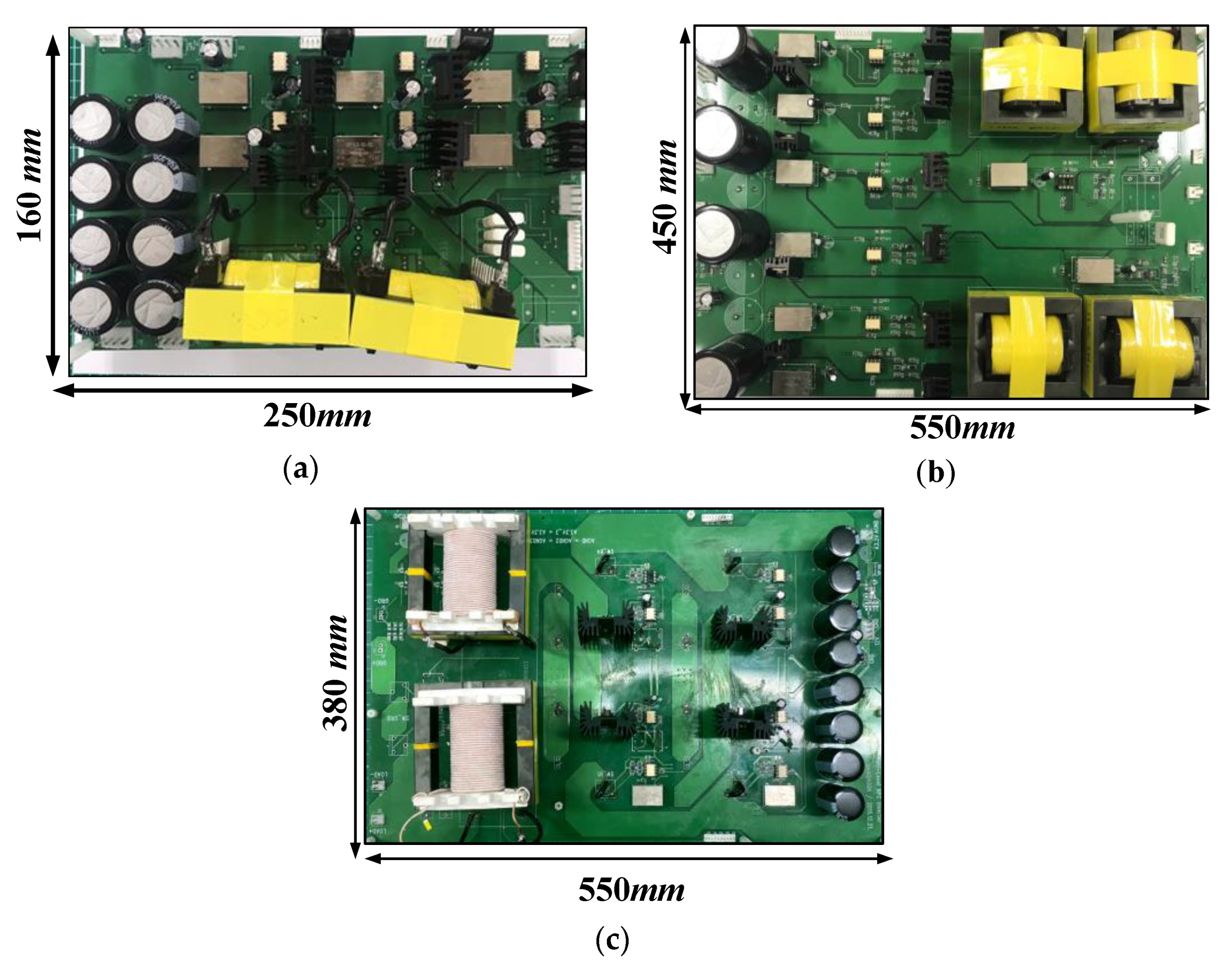
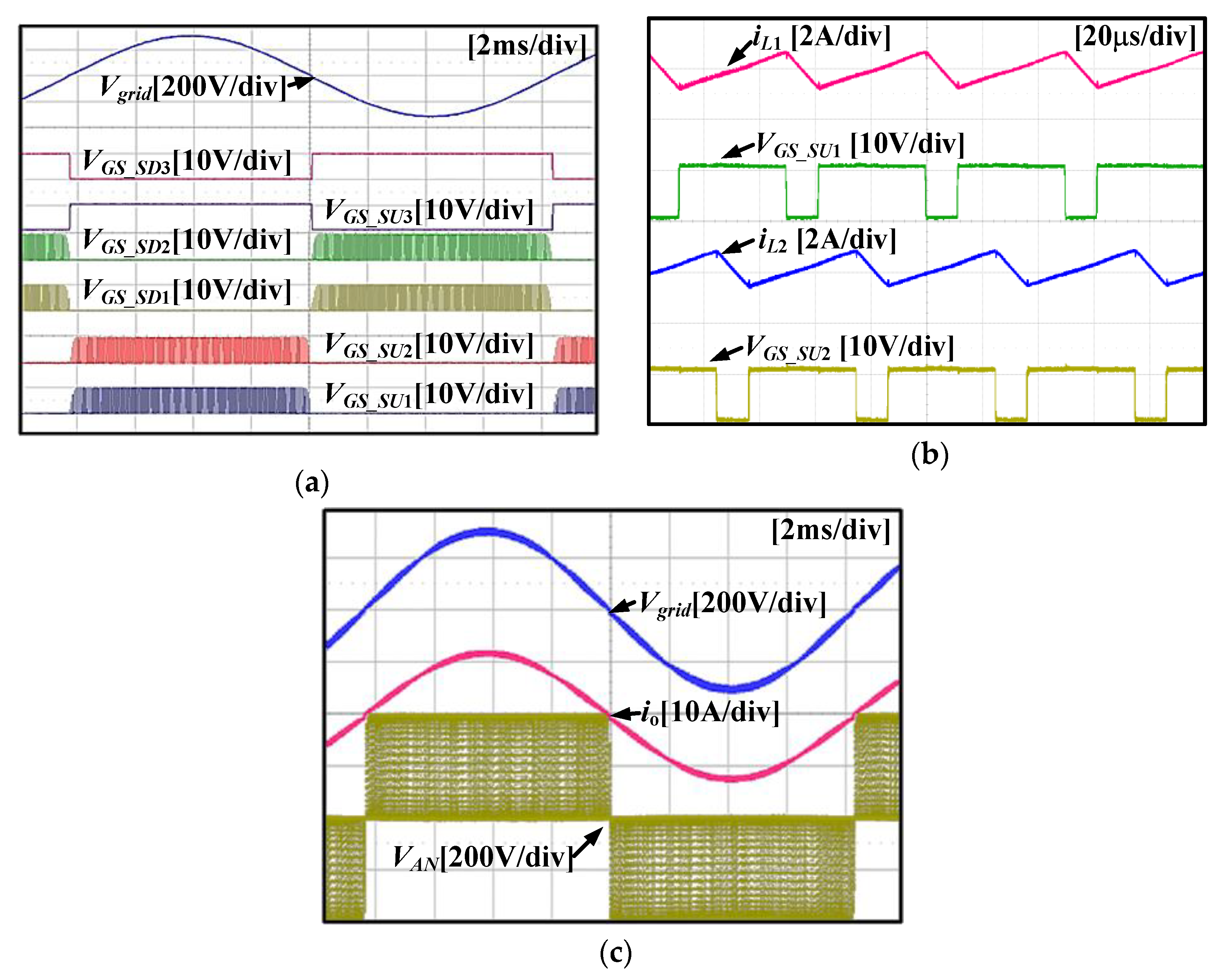
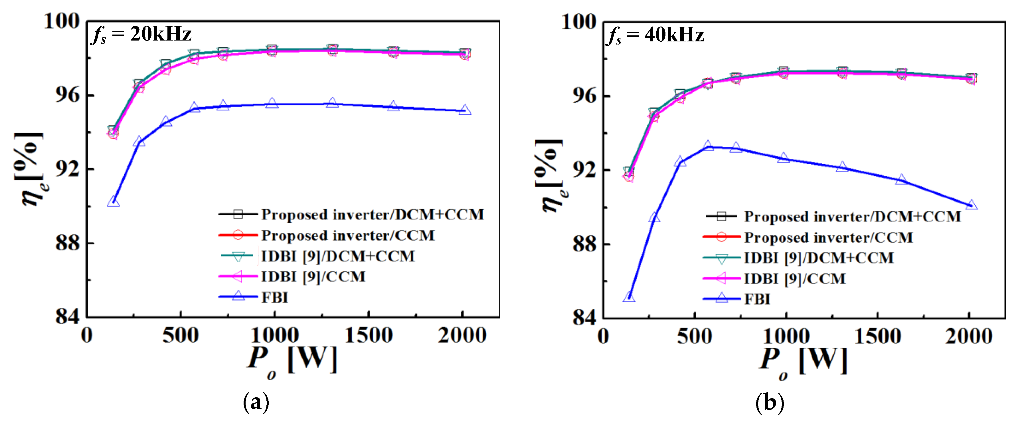
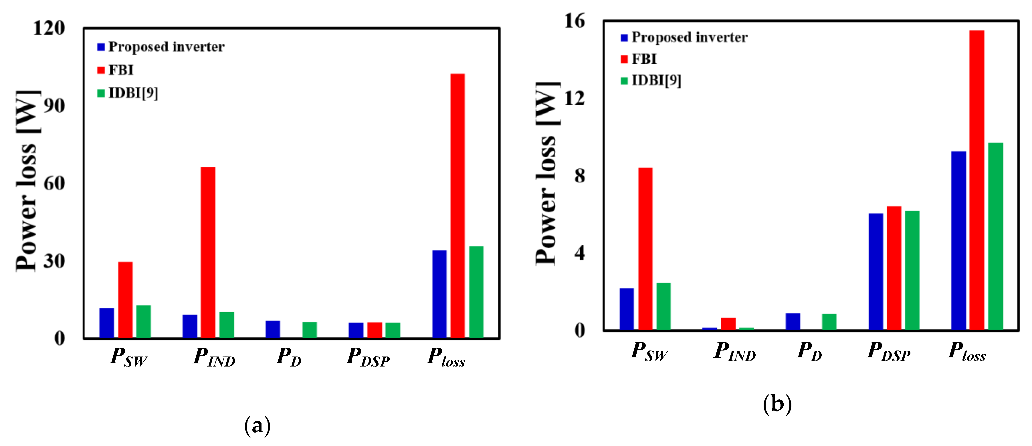
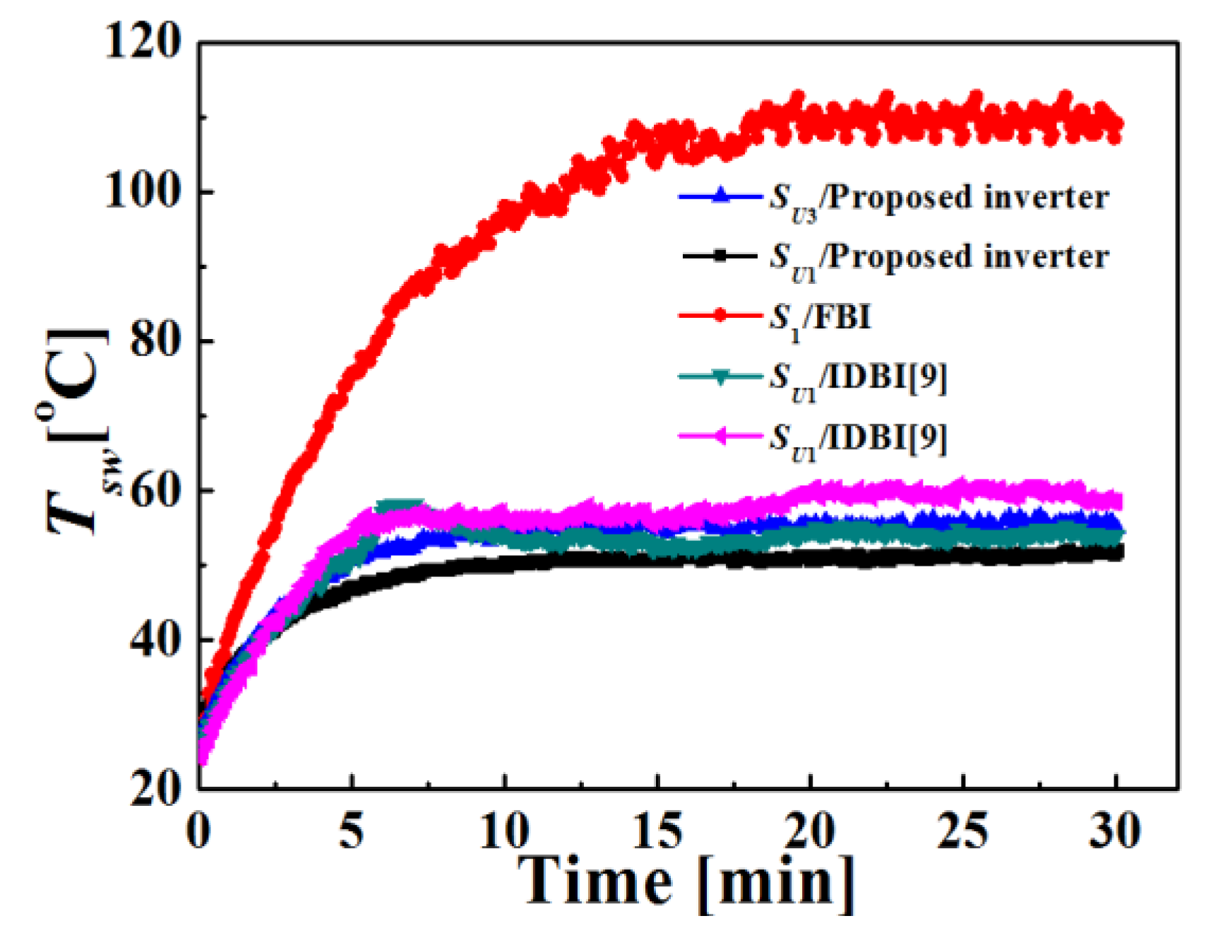
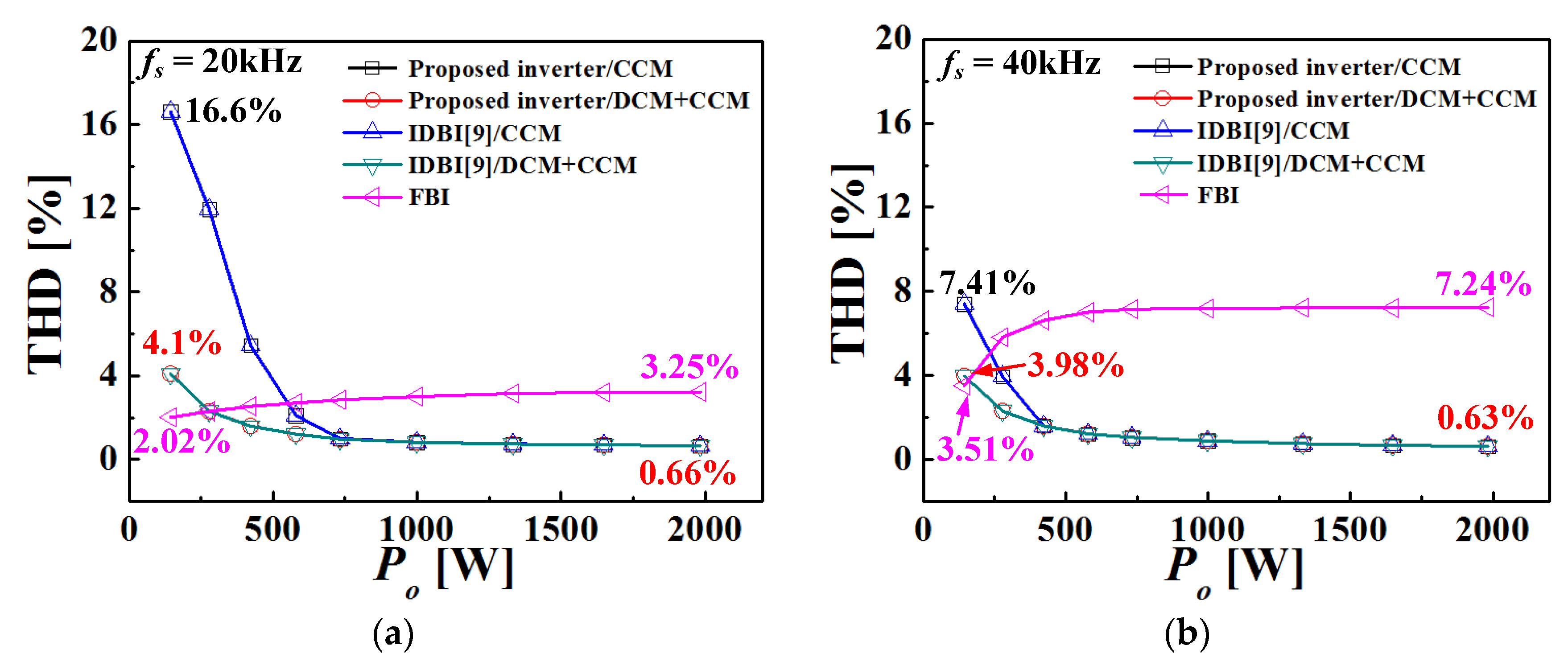
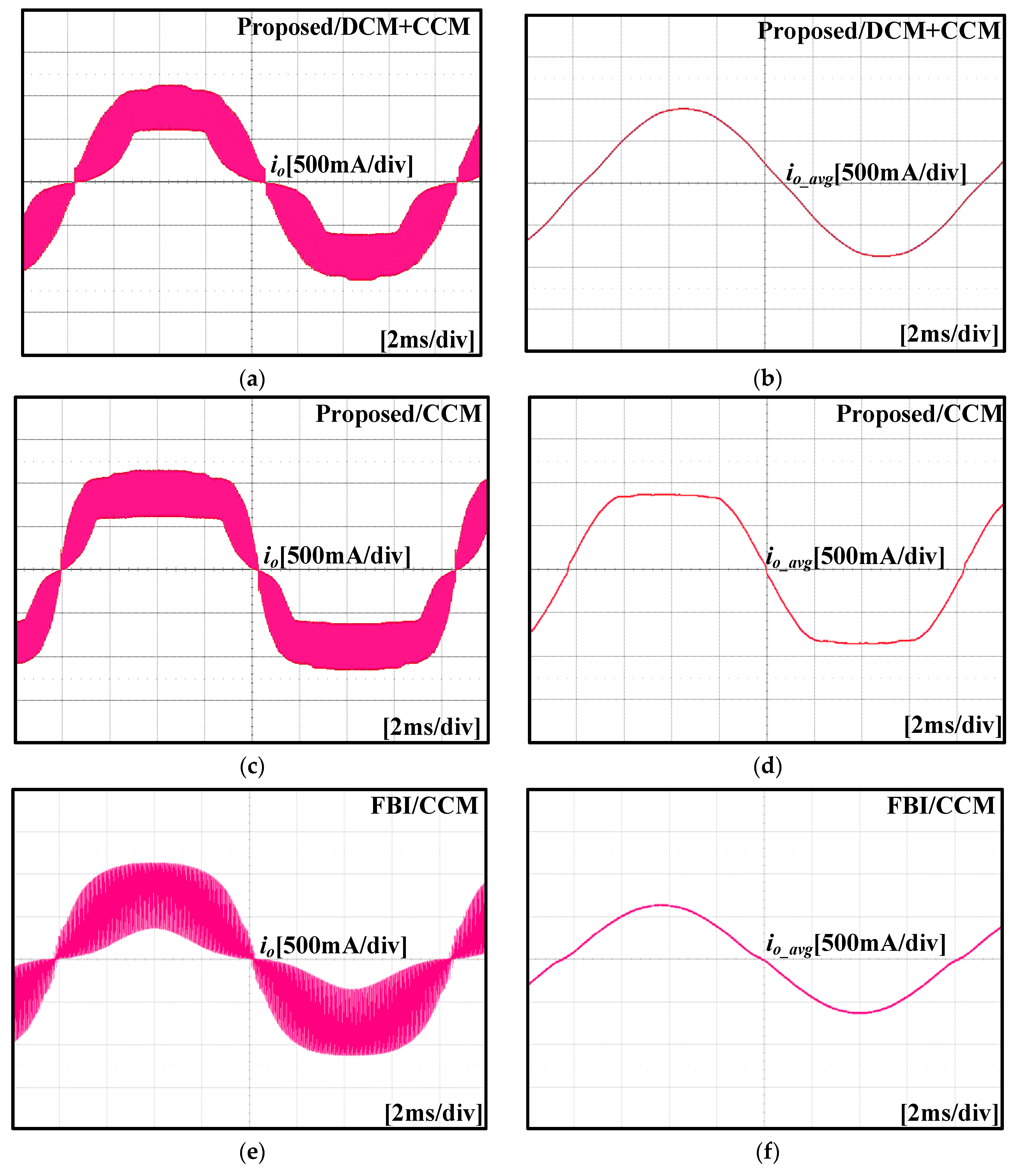
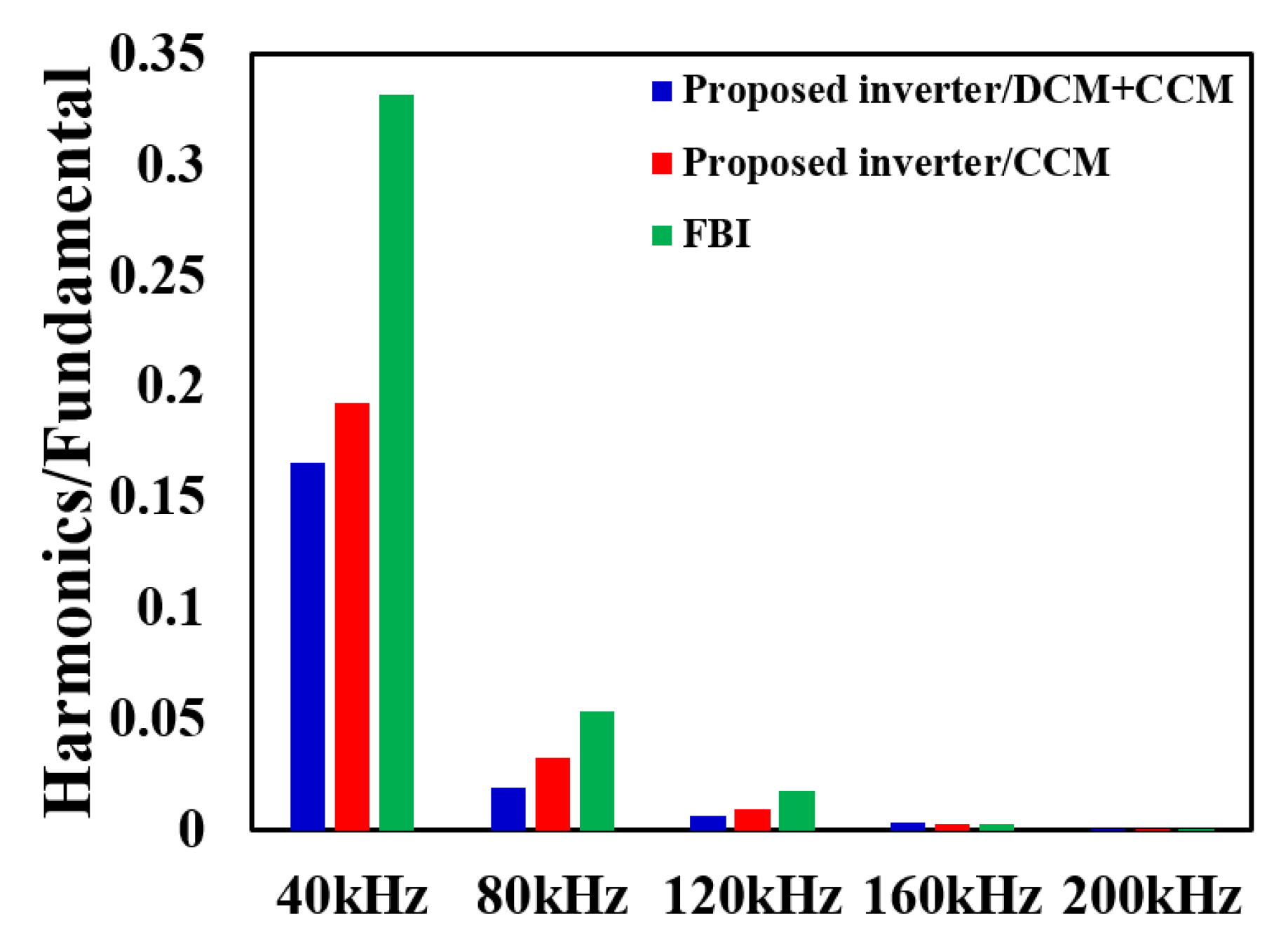
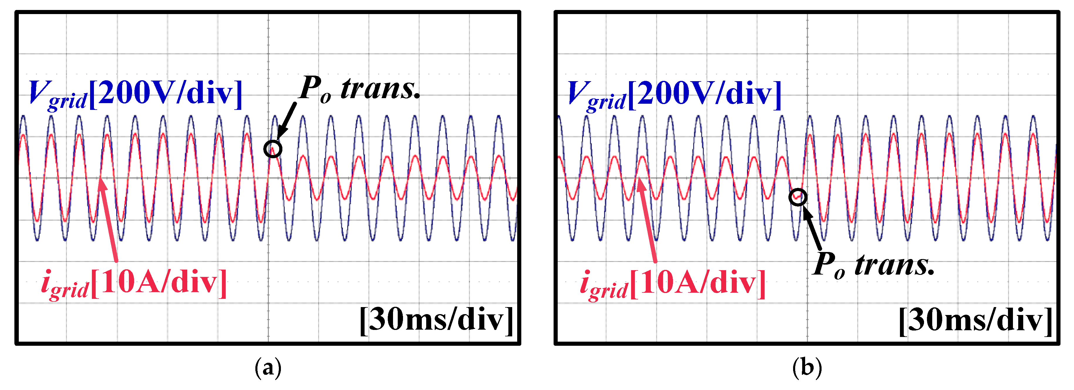
3. Experimental Results and Discussions

The proposed inverter (Figure 9a, Table 3) was designed to operate at Vin = 400 VDC, Vgrid = 220 VAC/60 Hz and 150 W ≤ Po ≤ 2 kW, and it was fabricated and tested using the calculated circuit parameters. An IDBI [9] (Figure 9b, Table 3) and an FBI [1] (Figure 9c, Table 3) were also fabricated and tested for comparison; the circuit elements for these inverters were the same as those for the proposed inverter. The control circuits for all experimental inverters were implemented using the TMS320F28335 digital signal processor (DSP) from Texas Instruments.
The proposed inverter uses two inductors, whereas the IDBI uses four inductors, and the proposed inverter uses a small inductor core (EER6062), whereas the FBI uses a large inductor core. The fabricated inverters had a circuit volume of 160mm × 250 mm × 43.9 mm for the proposed inverter, 450 mm × 550 mm × 43.9 mm for the IDBI, and 380mm × 550 mm × 78.0 mm for the FBI; the proposed inverter reduced 83.8% of the circuit volume compared with the IDBI, and 89.3% compared with the FBI. The circuit cost was $71.04 for the proposed inverter, $77.74 for the IDBI, and $73.9 for the FBI; the proposed inverter saved 8.62% of the circuit cost compared with the IDBI, and 3.87% compared with FBI.
To verify operation of the proposed inverter, the waveforms of switch-control pulses (Figure 10a) were measured at Vin = 400 VDC, Vgrid = 220 VAC/60 Hz, Po = 2 kW, and fs = 20 kHz. These waveforms show that the switches operated according to the switching states in Table 1; when Vgrid > 0 V, SU1 and SU2 operated in PWM mode, SU3 stayed ON and other switches stayed OFF; when Vgrid < 0 V, SD1 and SD2 operated in PWM mode, SD3 stayed ON and other switches stayed OFF. The inductor currents iL1 and iL2, and the leg voltages VGS_SU1 and VGS_SU2 (Figure 10b) show that the inverter operated in an interleaved mode; the phase differences between iL1 and iL2, and between VGS_SU1 and VGS_SU2 were Ts/2. These switching states produced the sinusoidal leg voltage VAN (Figure 10c).
η e vs. P o (Figure 11) was measured at Vin = 400 VDC, Vgrid = 220 VAC/60 Hz, 150 W ≤ Po ≤ 2 kW, and fs = 20 kHz and 40 kHz, using a PW3336 (HIOKI E.E. Co.) power meter. At fs = 20 kHz, the proposed inverter had η e > 98% for P o 500 W, but η e for P o < 500 W decreased as P o decreased because the inverter operated in DCM. The highest power conversion efficiency η e max of the proposed inverter was 98.5% at Po = 1300 W when the power loss PDSP of the gate control/drive circuit was included. ( η e max = 99.2% at Po = 500 W when PDSP was excluded.) The FBI does not use the interleaved buck inversion; hence, the switching and conduction losses in the current path were higher in the FBI than in the proposed inverter; as a result, the FBI had the lowest η e among the inverters tested. The IDBI has a circuit structure similar to the proposed inverter and operates in interleaved mode, so η e of the IDBI was very close to that of the proposed inverter. However, the proposed inverter requires two inductors to operate the inverter in interleaved mode, while the IDBI requires four inductors; hence, the proposed inverter can be implemented in a smaller size.
Losses (Figure 12) of the experimental inverters were analyzed at Vin = 400 VDC, Vgrid = 220 VAC/60 Hz, fs = 20 kHz, Po = 2 kW and 150 W, and reactive output power Qo = 0 volt-ampere-reactive (VAR). The switching losses PSW were 13.2 W for proposed, 13.89 W for IDBI, and 29.71 W for FBI at Po = 2kW, and PSW were 2.18 W for proposed, 2.48 W for IDBI, and 8.42 W for FBI at Po = 150 W. The inverters operated at VSW = Vin and NSW = 666 for proposed and IDBI, and VSW = Vin and NSW = 1333 for FBI, where Nsw is the total switching number for one cycle of Vgrid. Thus, the proposed inverter and IDBI had the lowest PSW. The inductor loss PIND was 9.25 W for proposed, 10.33 W for IDBI, and 66.32 W for FBI at Po = 2kW and 0.155 W for proposed, 0.162 W for IDBI, and 0.66 W for FBI at Po = 150 W. The proposed inverter uses interleaved inputs; hence, the inductor current iL is half of the iL of FBI. Moreover, the proposed inverter uses small inductors with fewer turns than that of the FBI. Thus, FBI had the highest PIND. The diode loss PD was 7.04 W for proposed, 6.45 W for IDBI, and 0 for FBI at Po = 2 kW, and PD was 0.907 W for proposed, 0.885 W for IDBI, and 0 for FBI at Po = 150 W. The power loss PDSP of the gate control/drive circuit was 6.02 W for proposed, 6.19 W for IDBI, and 6.48 W for FBI at both Po = 150 W and Po = 2 kW. The total power loss Ploss at Po = 2 kW was 35.53 W for proposed, 36.87 W for IDBI, and 102.51 W for FBI, and the power conversion efficiency η e at Po = 2 kW was 98.2% for proposed, 98.1% for IDBI, and 94.9 % for FBI. Ploss at Po = 150W was 9.279 W for proposed, 9.717 W for IDBI, and 15.5 W for FBI, and η e at Po = 150 W was 93.8% for proposed, 93.5% for IDBI, and 89.6 % for FBI.
The temperature T S W of switch vs. time of operation (Figure 13) was measured while operating the experimental inverters at Vin = 400 VDC, Vgrid = 220 VAC/60 Hz, Po = 2 kW, and fs = 20 kHz. T S W was stabilized at ~52 °C (SU1, SU2, SD1, SD2) and ~55 °C (SU3, SD3) in the proposed inverter, ~54 °C (SU1, SU2, SD1, SD2) and ~58 °C (SU3, SD3) in the IDBI, and at ~110 °C in FBI. PSW at Po = 2 kW were 13.2 W for proposed, 13.89W for IDBI, and 29.71 W for FBI; therefore, Tsw of the proposed inverter and IDBI was half that of FBI.
THD of i o vs. Po (Figure 14) was also measured at Vin = 400 VDC, Vgrid = 220 VAC/60 Hz, Po = 150 W ~ 2 kW, and fs = 20 kHz. THD at Po = 2 kW was 0.66% for proposed and IDBI and 3.25% for FBI; FBI had the highest THD because this inverter produced a ZCD during the dead-time period. THD at Po = 150 W was 16.6% for IDBI and the proposed inverter when the switching duties for the inverters were controlled using the CCM control (given in (8)). At a low Po, the proposed inverter operated in DCM for some time-interval of sinusoidal Vgrid, as discussed in Section 2.2. This operation produced a distortion in Io when the inverters were operated under CCM control only.
When the switching duties for IDBI and the inverters were controlled using the proposed DCM+CCM control (a combination of the CCM control and the DCM control given in Equation (7)), the THD at Po = 150 W was reduced to 4.1% because the combined DCM+CCM control reduced the distortion in Io significantly.
When fs was increased to 40 kHz, THD of io at Po = 2 kW was 0.63% for proposed and IDBI and 7.24% for FBI. The FBI nearly doubled the THD at fs = 40 kHz compared to the value at fs = 20 kHz, because the change increased the effect of dead-time on the switching duty. The THD at Po = 150 W was 7.41% for the proposed inverter using CCM control, 3.98% for the proposed inverter using DCM+CCM control, and 3.51% for FBI. The DCM operating time was reduced at higher fs (Equations (9) and (10)); hence, THD of the proposed inverter decreased as fs increased; a DCM control near the zero crossing point increased iL. In contrast, the THD for FBI increased as fs increased because the impact of dead-time on the switching duty increased.
The waveforms of io and io_avg for the experimental inverters (Figure 15) were measured at Vin = 400 VDC, Vgrid = 220 VAC/60 Hz, fs = 20 kHz, Po = 150 W, Qo = 0 VAR, and Io = 0.95 A. The cutoff frequency of the low-pass filter for io_avg measurement was 2 kHz (=fs/10). The inverters were controlled using CCM or DCM+CCM control. The waveforms of io show that the proposed inverter had the lowest switching ripple of io, and the waveforms of io_avg show that the DCM+CCM control of the proposed inverter achieved the best sinusoidal waveform. The harmonic components of io (Figure 16) show that harmonics of io of FBI were slightly higher than those of the proposed inverter because the proposed inverter operated as an interleaved dual buck inverter.
The dynamic responses of the proposed inverter (Figure 17) were measured for a step change of Po from 2 kW to 1 kW and a step change of Po from 1 kW to 2 kW; the operating conditions for this measurement were Vin = 400 VDC, Vgrid = 220 VAC/60 Hz, fs = 20 kHz, and Qo = 0 VAR. For both Po changes, the output current io did not overshoot, and the transient time of io was < 2 ms, which is ~1/8 of the sinusoidal period at 60 Hz. PF, THD, and io of the proposed inverter were measured for Po = 666.6 W, 1.333 kW, and 2 kW at Vin = 400 VDC, Vgrid = 220 VAC/60 Hz, fs = 20 kHz, and line impedance Z = 0.4 + j0.25 Ω. The measured PF was 0.9973 at Po = 666.6 W (33% of the rated power), 0.9985 at Po = 1.333 kW (66% of the rated power), and 0.9992 at Po = 2 kW (100% of the rated power). The measured THD of io was 4.20% at Po = 666.6 W, 3.68% at Po = 1.333 kW, and 3.43% at Po = 2 kW. These results fulfill most grid-connected inverter standards for renewable energy [19,20,21,22].
Comparisons (Table 4) of the circuit parameters and experimental results demonstrate the superiority of the proposed inverter. The proposed inverter has the following advantages: (1) proposed inverter requires two inductors, whereas IDBI requires four inductors; hence, the proposed inverter can be implemented with lower cost and smaller volume than IDBI; (2) it uses interleaved operation, which reduces the current stress of the switch by 1/2 of that in FBI; (3) the number of switching for one period of Vgrid in the proposed inverter is 1/2 of that in FBI; hence, the switching loss is reduced; and (4) η e at P o = 2 kW is as high as 98.3%, compared to 95.0% for FBI. These advantages indicate that the proposed inverter is useful for high-power dc-ac power conversion.

4. Conclusions

This paper proposes an inverter that can achieve high power conversion efficiency ηe at high output power Po. The inverter uses a dual-buck structure to eliminate zero-cross distortion, operates in an interleaved mode to reduce the current stress of switch, and uses DCM + CCM combined control to reduce the output current distortion at low output power. The size and weight of the circuit are reduced by decreasing the number of inductors and by using blocking diodes; the proposed inverter could reduce 83.8% of the circuit volume compared with IDBI and 89.3% compared with FBI, and it could save 8.62% of the circuit cost compared with IDBI and 3.87% compared with FBI. When the experimental inverter was operated at an input voltage of 400 VDC, an output voltage of 220 VAC/60 Hz, and switching frequency of 20 kHz, ηe was > 94% at 150 W ≤ Po ≤ 2 kW, 98.5% at Po = 1300 W, and 98.3% at Po = 2 kW. The total harmonic distortion was 0.66% at Po = 2kW. The proposed inverter is well-suited for high power dc-ac power conversion.

Author Contributions

M.-G.C. developed the circuit, constructed the hardware prototype, and conducted the experiments. B.K. provided guidance and key suggestions for this study. S.-H.L., H.-S.L., and Y.-G.C. collected the data and investigated early works. All authors have read and agreed to the published version of the manuscript.

Funding

This research was supported by the Ministry of Science and ICT(MSIT), Korea, under the “ICT Consilience Creative program” (IITP-2019-2011-1-00783) supervised by the Institute for Information & Communications Technology Planning & Evaluation (IITP).

Conflicts of Interest

The authors declare no conflict of interest.

Nomenclature

C 1 C 4 Output of comparators in the PWM generator.
D Switching duty of the proposed inverter.
D d Amplitude of D S U 1 parallel to V g r i d .
D D 1 , D D 2 Low-side freewheeling diodes of the proposed inverter and IDBI [9].
D q Amplitude of D S U 1 orthogonal to V g r i d .
D S U 1 Switching duty of S U 1 in the proposed inverter.
D U 1 , D U 2 High-side freewheeling diodes of the proposed inverter and IDBI [9].
D U 3 , D D 3 Blocking diodes of the proposed inverter.
e d , e q Control errors of I o _ d and I o _ q in the D-Q axis controller (A).
e θ Estimation error of θ ^ in the phased locked loop (rad).
f c l k , T c l k Clock frequency (Hz), and period (s) of TMS320F28335 digital signal processor.
f s , T s Switching frequency (Hz) and period (s).
i L 1 , i L 2 Inductor currents of the proposed inverter (A).
i L 1 _ a v g , i L 2 _ a v g Time average of i L 1 and i L 2 of the proposed inverter (A).
I o Amplitude of i o _ a v g (A).
i o _ a v g Time averaged value of the output current io for one switching period (A).
I o _ d Amplitude of i o _ a v g parallel to V g r i d (A).
I o _ d _ r e f , I o _ q _ r e f Reference values of I o _ d and I o _ q for the D-Q axis controller (A).
I o _ q Amplitude of i o _ a v g orthogonal to V g r i d (A).
i o _ r i p p l e Ripple in output current of the proposed inverter (A).
k p , k i Control coefficients94768 for the D-Q axis controller.
k p _ p l l , k i _ p l l Control coefficients for the phased locked loop.
L 1 , L 2 Output filter inductors (H).
n , j Sampling and clock sequence numbers.
RefReference input for the comparator array in the PWM generator.
S 1 S 4 High frequency switches of FBI [1].
S c , S c p Counter outputs for PWM.
S D 1 , S D 2 Low-side high frequency switches of the proposed inverter and IDBI [9].
S D 3 Low-side unfolding switch of the proposed inverter and IDBI [9].
S U 1 , S U 2 High-side high frequency switches of the proposed inverter and IDBI [9].
S U 3 High-side unfolding switch of the proposed inverter and IDBI [9].
T s w Temperature of switches (°C).
V A N Leg voltage with respect to the ground (V).
V A N _ a v g Time averaged value of V A N for one switching period (V).
V A N _ d Amplitude of V A N _ a v g parallel to V g r i d (V).
V A N _ q Amplitude of V A N _ a v g orthogonal to V g r i d (V).
V g Amplitude of V g r i d (V).
V g r i d AC output voltage (AC grid voltage) (V).
V i n DC input voltage (V).
V L 1 , V L 2 Voltages across the output filter inductors L1 and L2 (V).
V L 1 _ a v g , V L 2 _ a v g Time averaged values of V L 1 and V L 2 for one switching period (V).
Δ D Difference of switching duties for CCM and DCM operations.
Δ T s Duration of i L 1 ( t ) 0 for one switching period (s).
θ Phase angle of V g r i d (rad).
θ ^ Estimated θ by the phased locked loop (rad).
η e Power conversion efficiency of inverters.
ω Angular frequency of V g r i d (rad/s).
ω s e t Nominal value of ω (rad/s).

References

  1. Mazumder, S.K.; Nayfeh, A.H.; Boroyevich, D. Theoretical and experimental investigation of the fast—and slow-scale instabilities of a DC–DC converter. IEEE Trans. Power Electron. 2001, 16, 201–216. [Google Scholar] [CrossRef]
  2. Hwang, S.; Kim, J. Dead time compensation method for voltage-fed PWM inverter. IEEE Trans. Energy Convers. 2010, 25, 1–10. [Google Scholar] [CrossRef]
  3. Herran, M.A.; Fischer, J.R.; Gonzalez, A.; Judewicz, M.G.; Carrica, D.O. Adaptive dead-time compensation for grid-connected PWM inverters of single-stage PV systems. IEEE Trans. Power Electron. 2013, 28, 2816–2825. [Google Scholar] [CrossRef]
  4. Kang, F.S.; Park, S.-J.; Cho, S.E.; Kim, C.U.; Ise, T. Multilevel PWM inverters suitable for the use of stand-alone photovoltaic power systems. IEEE Trans. Energy Convers. 2005, 20, 906–915. [Google Scholar] [CrossRef]
  5. Zhou, J.; Huang, C.; Cheng, C.; Zhao, F. A Comprehensive Analytical Study of Dielectric Modulated Drift Regions—Part I: Static Characteristics. IEEE Trans. Electron. Devices 2016, 63, 2255–2260. [Google Scholar] [CrossRef]
  6. Araújo, S.V.; Zacharias, P.; Mallwitz, R. Highly Efficient Single-Phase Transformerless Inverters for Grid-Connected Photovoltaic Systems. IEEE Trans. Ind. Electron. 2010, 57, 3118–3128. [Google Scholar] [CrossRef]
  7. Yao, Z.; Xiao, L.; Yan, Y. Control strategy for series and parallel output dual-buck half bridge inverters based on DSP control. IEEE Trans. Power Electron. 2009, 24, 434–444. [Google Scholar]
  8. Liu, J.; Yan, Y. A Novel Hysteresis Current Controlled Dual Buck Half Bridge Inverter. In Proceedings of the IEEE 34th Annual Conference on Power Electronics Specialists (PESC), Acapulco, Mexico, 15–19 June 2003; IEEE: Piscataway, NJ, USA, 2003; pp. 1615–1620. [Google Scholar]
  9. Hong, F.; Liu, J.; Ji, B.; Zhou, Y.; Wang, J. Interleaved Dual Buck Full-Bridge Three-Level Inverter. IEEE Trans. Power Electron. 2016, 31, 964–974. [Google Scholar] [CrossRef]
  10. Zhou, L.W.; Gao, F. Dual Buck Inverter with Series Connected Diodes and Single Inductor. In Proceedings of the 2016 IEEE Applied Power Electronics Conference and Exposition (APEC), Long Beach, CA, USA, 21 March 2016; IEEE: Piscataway, NJ, USA, 2016; pp. 2259–2263. [Google Scholar]
  11. Hong, F.; Liu, J.; Ji, B.; Zhou, Y. Single Inductor Dual Buck Full-Bridge Inverter. IEEE Trans. Ind. Electron. 2015, 62, 4869–4877. [Google Scholar] [CrossRef]
  12. Zhou, L.; Gao, F. Improved Transformerless Dual Buck Inverters with Buffer Inductors. In Proceedings of the 2016 IEEE Applied Power Electronics Conference and Exposition (APEC), Long Beach, CA, USA, 21 March 2016; IEEE: Piscataway, NJ, USA, 2016; pp. 2935–2941. [Google Scholar]
  13. Yang, M.K.; Kim, Y.J.; Choi, W.Y. Power Efficiency Improvement of Dual-Buck Inverter with SiC Diodes using Coupled Inductors. In Proceedings of the 2018 IEEE 6th Workshop on Wide Bandgap Power Devices and Applications (WiPDA), Atlanta, GA, USA, 31 October–2 November 2018; pp. 56–59. [Google Scholar]
  14. Nguyen, T.T.; Cha, H.Y.; Nguyen, B.L.; Kim, H.G. A Novel Single-Phase Three-Level Dual-Buck Inverter. IEEE Trans. Power Electron. (accepted). [CrossRef]
  15. Kow, B.; Wei, J.; Zhang, L. Switching and Conduction Losses Reduction of Dual Buck Full Bridge Inverter through ZVT Soft-Switching under Full-Cycle Modulation. IEEE Trans. Power Electron. (accepted).
  16. Johnson, J. Improving Buck Converter Light-Load Efficiency. Power Electron. Eur. 2015, 5, 17–18. [Google Scholar]
  17. Zhang, R.; Cardinal, M.; Szczesny, P.; Dame, M. A grid simulator with control of single-phase power converters in D-Q rotating frame. In Proceedings of the 2002 IEEE 33rd Annual IEEE Power Electronics Specialists Conference (PESC), Cairns, QLD, Australia, 23–27 June 2002; pp. 1431–1436. [Google Scholar]
  18. Nise, N.S. Chapter 4, Time response. In Control System Engineering, 4th ed.; Dumas, S., Kulesa, T., Sayre, D., Eds.; John Wiley & Sons, Inc.: Hoboken, NJ, USA, 2004; Volume 1, pp. 198–201. [Google Scholar]
  19. VDE Association for Electrical Electronic and Information Technologies. VDE-AR-N 4105:2011-08 Power Generation Systems Connected to the Low-Voltage Distribution Network; VDE Association for Electrical, Electronic and Information Technologies: Frankfurt, Germany, 2011. [Google Scholar]
  20. IEEE Standards Association. IEEE 1547 Standard for Interconnecting Distributed Resources with Electric Power Systems; IEEE Standards Association: Piscataway, NJ, USA, 2003. [Google Scholar]
  21. Korean Agency for Technology and Standards. SGSF-04-2012-07 General Performance Requirements of PCS (Power Conditioning System) for Energy Storage Systems; Smart Grid Standardization Forum: Seoul, Korea, 2012. [Google Scholar]
  22. Operation Directorate of Energy Network Association. Engineering Recommendation G83, Issue 2; Energy Networks Association: London, UK, 2012. [Google Scholar]
Figure 1. Circuit structure of dc-ac inverters: (a) full-bridge inverter (FBI) and (b) interleaved dual-buck inverter of [9] (IDBI [9]).
Energies 13 01531 g001
Figure 2. Circuit structure of the proposed inverter.
Energies 13 01531 g002
Figure 3. Simplified gate signals of the proposed inverter.
Energies 13 01531 g003
Figure 4. Theoretical waveforms and circuit diagrams for leg 1: (a) VL1 and iL1 for DCM and CCM operation, (b) circuit diagrams for Mode 1, (c) circuit diagrams for Mode 2, and (d) circuit diagrams for Mode 3.
Energies 13 01531 g004
Figure 5. Block diagram of the control circuit for the proposed inverter.
Energies 13 01531 g005
Figure 6. Block diagram of the phase locked loop.
Energies 13 01531 g006
Figure 7. Block diagram of the D-Q axis controller.
Energies 13 01531 g007
Figure 8. Block diagram of the gate pulse generator.
Energies 13 01531 g008
Figure 9. Photographs of the experimental inverters: (a) proposed inverter, (b) interleaved dual buck inverter (IDBI), and (c) full bridge inverter (FBI).
Energies 13 01531 g009
Figure 10. Experimental waveforms of proposed inverter, measured at Vin = 400 VDC, Vgrid = 220 VAC/60 Hz, fs = 20 kHz, and Po = 2 kW: (a) gate input pulses, (b) VGS_SU1, V GS_SU2, iL1, and iL2, and (c) io, VAN, and Vgrid.
Energies 13 01531 g010
Figure 11. ηe vs. Po for the experimental inverters operating at (a) fs = 20 kHz and (b) fs = 40 kHz: measured at Vin = 400 VDC, Vgrid = 220 VAC/60 Hz, and Qo = 0 VAR. The power loss PDSP in the control circuit was included in ηe measurement.
Energies 13 01531 g011
Figure 12. Power losses in the experimental inverters at (a) Po = 2 kW and (b) Po = 150W: calculated using PSPICE at Vin = 400 VDC, Vgrid = 220 VAC / 60 Hz, fs = 20 kHz, and Qo = 0 VAR.
Energies 13 01531 g012
Figure 13. Switch temperature TSW vs. time of operation, measured at Vin = 400 VDC, Vgrid = 220 VAC/60 Hz, fs = 20 kHz, Po = 2 kW, and Qo = 0 VAR.
Energies 13 01531 g013
Figure 14. Total harmonic distortion (THD) of io vs. Po for the experimental inverters operating at (a) fs = 20 kHz and (b) fs = 40 kHz: measured at Vin = 400 VDC and Vgrid = 220 VAC/60 Hz.
Energies 13 01531 g014
Figure 15. Waveforms of io and io_avg measured at at Vin = 400 VDC, Vgrid = 220 VAC / 60 Hz, fs = 20 kHz, Po = 150 W, Qo = 0 VAR, and Io = 0.95 A: (a) io (Proposed, DCM+CCM), (b) io_avg (Proposed, DCM+CCM), (c) io (Proposed, CCM), (d) io_avg (Proposed, CCM), (e) io (FBI, CCM), (f) io_avg (FBI, CCM).
Energies 13 01531 g015
Figure 16. Harmonic components of io; measured at Vin = 400 VDC, Vgrid = 220 VAC/60 Hz, fs = 20 kHz, Po = 150 W, Qo = 0 VAR, and Io = 0.95 A.
Energies 13 01531 g016
Figure 17. Step responses of the proposed inverter at Vin = 400 VDC, Vgrid = 220 VAC/60 Hz, fs = 20 kHz, and Qo = 0 VAR: (a) for a decrease of Po from 2 kW to 1 kW and (b) for an increase of Po from 1 kW to 2 kW.
Energies 13 01531 g017
Table 1. Switching states and input voltages for inductors in the proposed inverter.
Vgrid≥0 V<0 V
SU1ON/OFFOFF
SU2ON/OFFOFF
SU3ONOFF
SD1OFFON/OFF
SD2OFFON/OFF
SD3OFFON
VAN_onVinVin
VAN_off00
Table 2. Input and output relationship of comparator array.
Outputi + nin
C1Ref[n]Sc[j]
C2Ref[n]Scp[j]
C3Vgrid[n]0
C40Vgrid[n]
Table 3. Components for the experimental inverters.
ComponentsIDBI [9]FBIProposed Inverter
HF SwitchesNameFCH110N65FFCH110N65FFCH110N65F
Price ($)5.035.035.03
Number4 (SU1, SU3, SD1, SD2)4 (S1 - S4)4 (SU1, SU3, SD1, SD2)
LF SwitchesNameIXFK80N60P3-IXFK80N60P3
Price ($)5.03-5.03
Number2 (SU3, SD3)-2 (SU3, SD3)
DiodesName30ETH06-30ETH06
Price ($)1.59-1.59
Number4 (DU1, DU2, DD1, DD2)-6 (DU1DU3, DD1DD3)
Inductor corePart NameEER6062EC90EER6062
Price ($)4.9416.174.94
Number422
Electrolytic capacitorPart NameEKMR451VS N681MA50SEKMR451VS N681MA50SEKMR451VS N681MA50S
Price ($)2.682.682.68
Number888
Total costs ($)77.7473.971.04
Table 4. Circuit parameters and experimental results for experimental inverters. Parenthesis contain peak switch voltages and currents measured at Vin = 404 V.
Circuit ParametersProposed InverterIDBI [9]FBI
# of switches664
# of diodes640
# of inductors242
Vsw,maxUnfoldingVin (404 V)Vin (404 V)-
SwitchingVin (413 V)Vin (415 V)Vin (423 V)
Isw,maxUnfoldingIo (13.1 A)Io (13.5 A)-
SwitchingIo/2 (5.8 A)Io/2 (6.0 A)Io (13.5 A)
Inductance2.5 mH2.5 mH2.5 mH
THD at Po = 2 kW0.66%0.66%3.25%
Maximum efficiency98.5%98.4%95.2%
Efficiency at Po = 2 kW98.3%98.2%95.0%

