Article

From Non-Modular to Modular Concept of Bidirectional Buck/Boost Converter for Microgrid Applications

Department of Mechatronics and Electronics, Faculty of Electrical Engineering and Information Technologies, University of Zilina, 01026 Zilina, Slovakia
*
Author to whom correspondence should be addressed.
Energies 2020, 13(12), 3287; https://doi.org/10.3390/en13123287
Submission received: 30 May 2020 / Revised: 23 June 2020 / Accepted: 24 June 2020 / Published: 26 June 2020
(This article belongs to the Special Issue Advanced DC-DC Power Converters and Switching Converters)

Abstract

:
In this article, the practical comparison of the operational performance of the modular (or multiport) and non-modular bidirectional buck/boost (bi-BB) DC/DC converter is realized. The main contribution of the work is the evaluation of both concepts based on various aspects, considering the qualitative indicators of the systems relevant for microgrids. Here, we discuss efficiency, electrical properties, costs, and component values. At the same time, critical comparisons are provided for converters based on SiC and GaN technology (non-modular high-voltage SiC-based dual-interleaved converter and modular low-voltage GaN-based). The concepts are specific with their operating frequency, whereby for each solution, the switching frequency is different and directly influences relevant components. The efficiency, overall system volume, output voltage ripple, and input current ripple are compared mutually between both concepts with a dependency on power delivery. These factors, together with overall volume and costs, are very important considering modern converters for microgrid systems. The summary of pros and cons is realized for each of the proposed converters, whereby the evaluation criterion is reflected within the electrical properties targeting microgrid application.

1. Introduction

Electricity generation, transmission, and distribution are being revolutionized due to various economic, technical, and environmental reasons. A microgrid (MG) is among the new technologies that have attracted great attention recently. The existing centralized grid system is actively being replaced by distributed energy resources located closer to consumers to meet their requirements effectively and reliably. A microgrid is a modern distributed power system using local, sustainable power resources designed through the various smart grid in initiatives. Energy resources such as small capacity hydro units, wind turbines, and photovoltaic systems, in cooperation with energy storage systems, are within MG for electrification. Here, we discuss mainly households where grid electricity access is not simple due to poor access to remote areas or technical skills [1,2,3,4].
A DC-based microgrid is one of the proposed architectures for geographically remote users. The considered architecture can investigate the performance and feasibility of a DC-based microgrid for the small domestic area, as illustrated in Figure 1. In this model, several types of sources, such as solar energy, a wind power generator, or an energy storage system (ESS), are connected to the DC distribution node. Each energy source is connected to a common DC node through a relevant power converter. For example, a wind generator uses an AC/DC isolated PFC converter; solar panels use MPPT boost converters; and ESS is mostly equipped by bidirectional buck/boost topology to deliver energy into DC distribution bus. The DC bus is connected to different types of load, which may require power in the form of DC or AC and can be achieved by using DC/DC buck or DC/AC converters [5,6]. Decentralized energy sources can also be considered in the context of electric vehicle batteries, which can also serve as an energy storage system if needed. For such distribution and proper cooperation of individual ESSs, the network must allow bi-directional power flow between them and even between them and DC bus [7,8].
Bidirectional energy flow between the DC bus and ESS can be secured by a wide spectrum of power converter topologies, among which the buck/boost converter is mostly utilized due to definitions on input/output operational parameters [8,9,10,11]. Even bidirectional buck/boost (bi-BB) topology exhibits many variations (considering isolation, soft-switching, etc.); it is recommended to utilize the robust, reliable, redundant, and efficient solution. Simultaneously, such a solution shall not require high investments and cost for design and development [12,13,14,15,16].
Due to the mentioned fact, this paper focuses on the more detailed investigation and analyses of standard bidirectional buck/boost converter (two alternatives). At the same time, the main criterion of the evaluation is reflected within efficiency performance, costs, and input/output ripple of electrical variables. Here, an interleaved non-modular solution of a bi-BB converter equipped with SiC technology is compared to modular solution equipped by GaN transistors. Concepts differ in power semiconductor technology; thus, operating frequency and power level of individual modules comprising the whole converter system are specific for both types. For the evaluation of pros and cons, specifications on operational parameters have been defined considering DC microgrid subpart ESS–BiBB converter–DC bus. Due to purposes of laboratory testing, the converters are prototyped in a reduced power ratio, i.e., 1:10 related to power delivery and electric stress (reflected in power losses). A detailed evaluation of both technological concepts is provided, while key evaluation criteria are subjected to the main specifics of the microgrid systems (concept flexibility, complexity). The major contribution is focused on the mutual evaluation of SiC technology and GaN technology from the perspective of the application scope. In contrast, such evaluation concerning the functionality of the target application was not carried out in detail in already published studies [17,18,19,20,21].

2. Bi-BB Converter from Non-Modular to Modular Topology—Properties Analysis

For the purposes of the analyses related to the design of a microgrid’s ESS power converter system, the focus is given on the determination of electrical properties of non-isolated bidirectional buck/boost alternative, whose principal diagram is shown on Figure 2 [4]. Since interleaved topologies are becoming increasingly utilized due to the number of positives, here we consider dual interleaved bi-BB converter as non-modular topology (Figure 3). The modular concept of n-modules will be composed of standard bi-BB converter (Figure 3), while the means of the connection of input/output terminals is described later within text.
Investigation of the waveforms of voltages and currents might be considered for the output and input parts of the converter as well. Regarding current ripples, they influence the effective value of current of the output capacitor, what affects its lifetime. Therefore, analyses according to current ripples must be provided if the optimized operation of the converter is the target [22,23,24].

Current/Voltage Ripple Dependencies

One module of the modular converter and one two-phase non-modular converter is depicted in Figure 3. The difference in the modular and non-modular converter is that the modular converter has modules connected in series, i.e., outputs are connected in series, and input sources are independent of each other. On the other side, the connection of modules in a non-modular converter is in parallel.
The assumption is that the inductor current is continuous in cases where the converter works in a boost or a buck mode, as shown in Figure 2. In a steady state, the inductor current is the sum of the DC and AC parts. If the condition of minimal value of input capacitor Equation (1) is satisfied [25], the input current drawn from the battery is constant. In this case, the AC component is provided by the capacitor current. Then, the AC component is equal to the ripple of the inductor current, Equations (2) and (3) [17], which are valid for the boost and a buck converter, respectively.
C m i n = Δ I L 8 f s w Δ V C I N
Δ I I N = Δ I L = Δ I C I N = V I N L f s w D
Δ I I N = Δ I L = Δ I C I N = V O U T V I N L f s w D
where Cmin is the minimal value of input capacitance, fsw is the switching frequency, ΔVCIN is the voltage ripple on the input capacitor, ΔIIN, ΔIL, and ΔICIN are the values of the ripple of the input current, the inductor and the input capacitor, respectively, VIN is the input supply voltage, D is the duty cycle, and VOUT is the value of the converter output voltage.
The inductor current ripple, Equation (2), is dependent on the input voltage (battery voltage), duty cycle, inductor value, and the switching frequency. A modular converter, unlike a non-modular one, has separate input sources. A non-modular converter has one input source or input source connected in series (e.g., serially connected battery packs). It means that the input voltage is much lower in the case of a modular converter, and therefore the current ripple is much smaller. This fact significantly reduces the ripple of the input current. Therefore, an inductance with a much smaller value is enough to maintain the same input ripple in comparison to the non-modular solution. For example, the n-module modular converter is used, and n-series connected battery packs are used for the non-modular case, the inductor value should be n times lower for the maintenance of the same current ripple.
The character of the input capacitor current for both converters is triangular, not impulse. Therefore, the impact on a voltage ripple is smaller than in the case of the impulse current. The input voltage ripple is dependent on an AC component of the inductor current and ESR of the battery pack and input capacitor. However, due to DC current drawn from the battery, as was mentioned earlier, and the parallel-connected battery pack with high capacity to the input capacitor, the input voltage ripple is negligible.
The topology of the non-modular converter is classical interleaved bidirectional buck/boost converter. In the case of interleaved topology, it is possible to achieve a state when the input current ripple is zero due to current ripple cancelation between parallel-connected phases [26,27,28]. This situation is depicted in Figure 4, [29]. The ratio between the input current and the inductor current is shown. It is an advantageous property in cases where the operation of the converter is at or around the desired duty cycle. In the case of a four-phase converter, the desired duty cycle is 0.25, 0.5, and 0.75. Ideally, the input voltage ripple is also zero or almost zero. It can be seen from Figure 4 that the ripple of the input current is smaller over the entire range of the duty cycle (ΔIL is also inductor current of the modular converter). This statement applies under the condition mentioned above, and the input voltage is the same for the modular and non-modular converter. A more detailed explanation of a current ripple for the interleaved topologies is given in Appendix A.
For a better image of the current and voltage ripple cancellation at the output of the modular converter, the simplification of the converter must be performed. If we simplify the given converter by the replacement of the output series-connected capacitor with one capacitor, then the current to this capacitor is continuous and does not have a pulse character (only triangular) during operation for up to 87.5% of the duty cycle. This operational mode is valid for modular concepts; thus, it meets this criterion. The value of the capacitor is then n times lower, and ESR is n times higher. The load current of the simplified converter (conventional bi-BB converter) is equal to the effective value of the capacitor current of the one module in the modular converter. The ripple of the output capacitor current is as follows:
Δ I C = V O U T V I N 8 L f s w
An explanation of the simplification and calculation of the output current ripple is given in Appendix B.
In the case of the non-modular converter, the output capacitor current is continuous when the value of the duty cycle is above 50%. Otherwise, the current has a pulse character, and the ripple is much higher. Therefore, the utilization of a modular converter is a better solution because the current ripple cancelation is within the wide operational range of the converter. The voltage ripple calculation is performed according to Equations (4) and (5), respectively [17].
Δ V C = Δ I C C f s w

3. Bi-BB Converter Design Guideline Considering Components Selection and Costs

Since the design of the bi-BB converter must be adjusted to the nominal parameters of the target application, the input specifications are exactly defined (Table 1). The target application is considered as a low-power installation of a smart-grid node within the family house. The primary source of energy from renewable energy types is the photovoltaic block (Figure 1), which supplies the MPPT converter, whose output supplies the DC bus with 600 V of nominal voltage, which represents the input side of the bi-BB converter. For the modular system, the input voltage is divided between the serial connection of the modular converter blocks (Figure 5).
The input voltage for both concepts shall be 600 V, thus for the non-modular solution, the output is single. In contrast, the modular solution is characterized by the serial connection of the input terminals of the individual converters. The output of bi-BB supplies energy storage components (battery pack). At the same time, the non-modular concept is defined by 520 V of single output voltage, whereby the modular concept has an n-independent low-voltage output connected to ESS. The advantage of a modular concept is the possibility of active battery management provided by individual modules of the concept, as it has an independent output connected to batteries. It improves power management and prolongs life expectations, as discussed in [30,31]. The non-modular solution shall be equipped by additional active/passive balancing units if required.
Focusing on the circuit component selection, the modular system may be based on the GaN technology of the semiconductor components. Such a solution is suitable due to the division of the power and voltages to separate individual modules in reduced merit. It also enables us to increase switching frequency several times. Such an approach might reduce the dimensions of used components (magnetic components, capacitors, PCB). Thanks to lower dimensions, it is possible to design converters with smaller PCB, while the volume of a complex modular system would be smaller compared to the non-modular system. Operational parameters of the non-modular system predetermine SiC technology as the main switching component. The switching frequency for these components can be higher compared to standard Si transistors, whereby, considering high voltage and power levels, it is not recommended due to efficiency reduction. Next, Equations (6)–(8) were used for the determination of the values of the main circuit components (Figure 3) affecting the converter volume.
Figure 6 shows the 3D dependency of the values of inductor L and filter capacitor COUT received using (6)–(8) for the situation when the number of modules and switching frequency vary [17]. At the same time, input/output parameters are relevant for individual module count.
  L [ H ] = V i n   ( V o u t V i n ) Δ i L   I o u t _ m a x   f s w   V o u t  
where Vin is the input converter voltage (V), Vout is the output converter voltage (V), fsw is the switching frequency (Hz), ΔiL is the ripple of inductor current (%), and Iout_max is the maximum output current (A).
  D [ % ] = 1 V i n _ m i n   V o u t  
where Vin_min is the minimum input converter voltage (V), and Vout is the output converter voltage (V).
  C o u t [ F ] = I o u t _ m a x   D Δ V o u t   f s w   V o u t
where Iout_max is the maximum output current (A), D is the duty cycle (%), fsw is the switching frequency (kHz), ΔVout is the ripple of the output voltage (%), and Vout is the output voltage (V).
It must be noted that the interpretation considers one module situation. For the whole modular solution, the result must be multiplied by the relevant number of the considered modules.
Table 2 shows input/output parameters that have been included within the calculation of the L and COUT if real operational conditions are valid. At this point, the need for semiconductor devices is considered for various scenarios. It is seen that for the non-modular solution, a high voltage SiC transistor module is needed. For two and four modules, high-voltage GaN transistors (650 V) must be used, while for a higher number of modules, it is allowed us to utilize 100 V GaN transistors.
At this place, the economic performance, together with efficiency and power density calculation, is given. Initially, Table 3 shows an expert estimation of the investments necessary for the design of proposed solutions of the bi-BB converter. The estimation considers with the whole bill of materials of electronic parts (power semiconductor components, drivers, magnetic components, passive components, and PCB), while the standard distribution network was considered. It is seen that the initial costs of the non-modular DC-DC interleaved converter based on the SiC technology are comparable to the initial costs that are relevant for up to a 16-stage modular DC-DC converter.
Figure 7 shows the graphical interpretation of the so-called qualitative parameters of power semiconductor converters with a dependency on switching frequency. Here, it was defined that these parameters are material costs, efficiency, and expected converter volume (concerning power delivery can be considered as power density). Initially, a non-modular solution is compared that has a dependency on switching frequency. It is seen that with the increase in the switching frequency, the costs together with volume decrease, which is related to the fact that smaller reactive components can be used within the converter’s main circuit. Efficiency is almost similar for each of the operating frequencies, as SiC transistors are suitable for the investigated range of this parameter.
Consequently, comparisons are provided between non-modular and modular concepts, while switching frequency is considered as 100 kHz. Considering the volume of the converter (power density), a non-modular solution exhibits performance that is most suitable regarding given switching frequency and input/output parameters that are limited due to power delivery and semiconductor performance (Figure 8). For high power levels, it is expected to operate at lower frequencies in order to prevent unwanted negative impacts (safety reasons, EMC, efficiency reduction, etc.). At the same time, robust semiconductors must be used (IGBT, SiC MOSFETS) [32,33,34].
The modular solution is not attractive for low switching frequencies due to a power density point of view, which influences the cost of such a solution. On the other side, it is seen that this parameter is best for the case of an eight-module solution. It is related to cheaper power components when the input/output voltage is reduced. Thus, components with lower current/voltage loading can be utilized, and a reasonable number of modules shall be selected (for 20 modules, the cost is very high due to the high number of components). Therefore, the high-switching frequency operation is easy to utilize.
Evaluation of the impact of switching frequency increase is reported in Figure 9 and Figure 10, where only modular solutions are compared for 500 kHz and 1 MHz. With this increase, the volume of the passive components can be visibly reduced. Moreover, when GaN technology is considered, the volume of the semiconductors also minimizes. A GaN-based converter system has a big advantage if a very small volume and weight are required. Typical examples are mobile systems, compact converter systems, or electromobility. From Figure 9 and Figure 10, it is seen that with the increase in switching frequency, the total volume of the modular converter system can be reduced below the volume of the non-modular solution, whereby this is valid from 500 kHz of switching frequency and above four numbers of the modules. The positive impact of frequency increase is the opposite if efficiency is evaluated. For 1 MHz of switching frequency, the efficiency drops below 93% if more than eight modules are used.

4. Comparison of Operational Properties of Proposed Eight Modules Bi-BB Modular Converter and Bi-BB Non-Modular Interleaved Converter

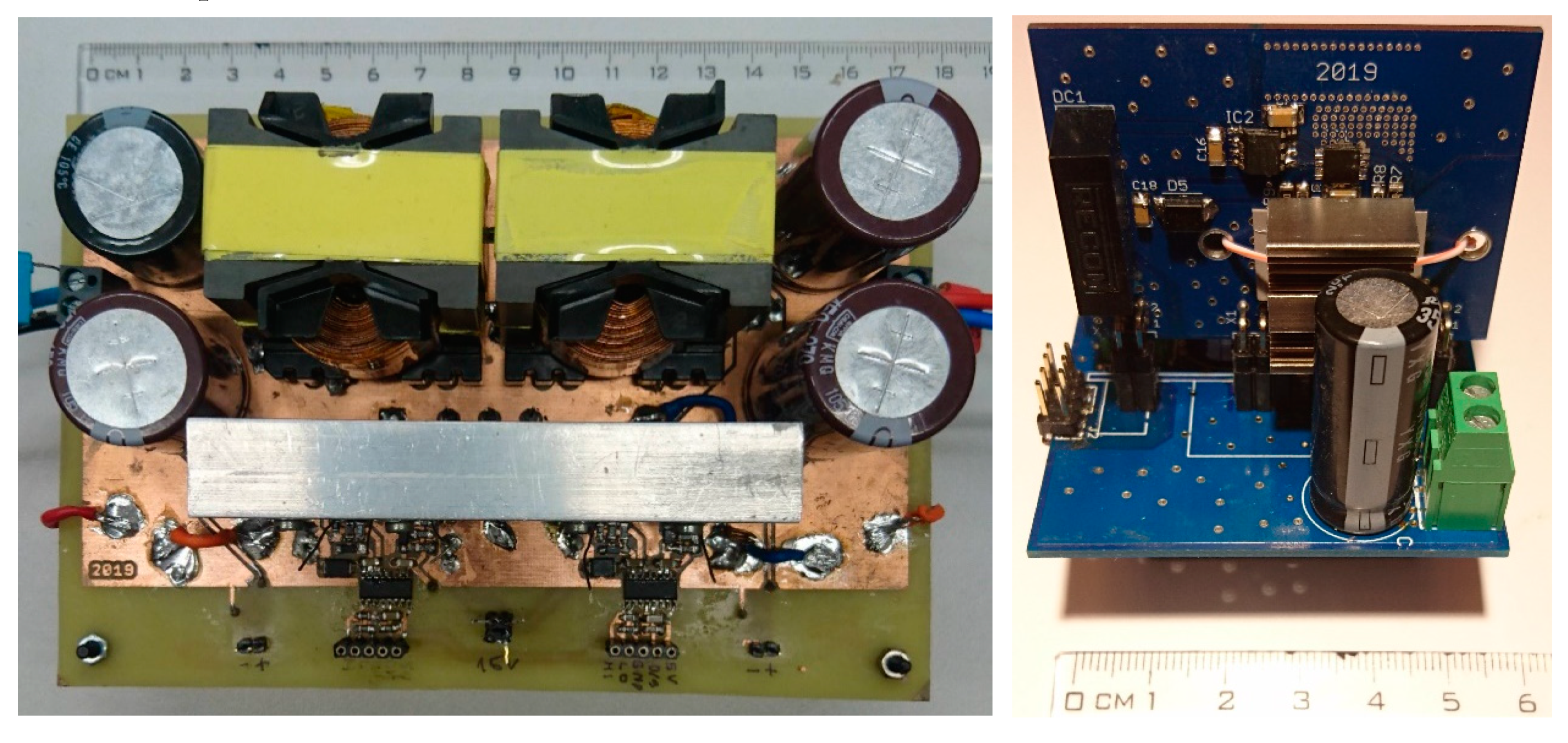
4.1. Concepts Description

Due to initial validation purposes, the parameters listed in Table 1 were reduced by the power ratio 1:10. Considering similar conditions to the real system, voltage levels were also modified for experimental prototypes of converters (Table 4). The block diagram (Figure 11) indicates the voltage levels selected for practical experiments, while the values are reduced for power delivery of 1 kW full power (the real system operates at 10 kW).
The converters in the modular solution are phase-shifted by 360/8° to achieve a low output voltage and current ripple. However, this power ratio emulation is also reflected within component design and selection of the converter’s main circuit devices in order to provide us with the most realistic conditions as possible. The non-modular concept utilizes SiC transistors operating at lower switching frequencies (app. 100 kHz) and uses standard inductors. On the other hand, in order to provide an increase in power density performance, the modular concept utilizes low voltage/high-speed GaN transistors (operating over 300 kHz) with planar inductors. This approach shall demonstrate the optimization possibilities of a bidirectional buck-boost converter using a modular converter concept.
The physical prototypes of the converters were designed based on parameters given in Table 4. Table 5 lists the main circuit components used within a non-modular and modular converter prototype.
Figure 12 shows a physical sample of proposed bi-BB converters. The non-modular concept uses inductors that are made on PQ40 N87 cores, while the winding is made of isolated copper foil in order to achieve low conduction losses. In order to secure the safe operation of the control system, the isolation on the side of gate drivers was used.
An experimental prototype of one module that is used for a modular concept, where eight converters with separate inputs and common output are connected to achieve the 200 V of the output voltage, is shown in Figure 12 as well. The proposed module consists of two boards. The horizontal motherboard is composed mostly of filtering components like electrolytic capacitors with MLCC capacitors and power inductors. The vertical board consists of GaN transistors with gate drivers, DC/DC isolated modules, optical isolators, and connector sockets. The vertical board is connected to the motherboard trough socket for better serviceability of measured parameters and more suitable electronic components maintenance.

4.2. Operation Properties Comparisons

The experimental measurements focused on the evaluation of main operational characteristics for both the buck and boost mode of designed bi-BB converter concepts. The evaluations were made separately for efficiency and voltage/current ripples. The laboratory equipment and experimental set-up used within measurements are shown in Figure 13.
For buck and boost mode, three input voltages were applied, while the investigated variables were analyzed for the whole output power range. Figure 14 shows the efficiency dependency for the boost mode, while the input voltage varied within 90 V and 110 V. Both tested solutions offer almost 97% efficiency, whereby the difference between analyzed converter types is visible in dependency on output power. The input voltage of the modular system is created by a sum of eight voltages on the inputs of individual modules. The efficiency decreases with the increase in output power, while on the other side, the non-modular system has increasing character. These facts are caused due to operational character, for example, due to the three times higher switching frequency of modular concept.
Even for the buck mode of operation, the modular system has a decreasing character of efficiency (Figure 15), which is also a cause of the higher number of switching transistors that are used. More transistors cause more hard switching losses and lower efficiency for higher output loads. If both efficiency characteristics for boost and buck mode are analyzed, the modular solution exhibits an advantage below 60% of the nominal power. In contrast, above this point, non-modular solutions become more effective.
Figure 16 shows the output current ripple of the systems in boost mode of operation. The modular system has a current ripple of around 1% and a non-modular system around 3% if nominal power is considered. From the diagram, it is seen that the modular concept has a lower ripple than a non-modular system within the whole power range. This fact is caused by the higher switching frequency in a modular system and interleaved operation given by the 360/8° ratio of control signals.
Figure 17 shows the output current ripple of the systems in the buck mode of operation. The modular system again reaches much lower values compared to the non-modular system, while the values of the ripple are below 0.5% if the output power is higher than 30% of the nominal converter’s power. During the change in the input voltage, a modular solution exhibits visible independence, while the non-modular system is visibly dependent if the ripple vs. input voltage is analyzed. The lowest ripple for the non-modular solution is achieved at a high output power, which is related to the extension of the duty cycle if the output power is increased.
Figure 18 and Figure 19 show the dependency of the output voltage ripple of both concepts in the boost and buck modes of operation. The modular system has a voltage ripple around 0.8% and a non-modular system around 1.6% at the nominal point of operation if buck mode is considered. For boost mode, the modular system has voltage ripple around 1% and the non-modular system around 1.8% at full power. If both operational modes are analyzed (buck and boost), the modular system has a better voltage ripple performance than a non-modular system for any voltage level applied at the input terminals of converters.
Previous analyses showed the advantages and disadvantages of the operational characteristics of designed bi-BB converters. Both have pros and cons related to costs, power density, efficiency performance, as well as the character of electrical variables. Related to the mentioned facts, it is further valuable to investigate the impact of previous research within the target application (i.e., microgrid), where designed converters are used as energy flow control blocks. Seeking higher flexibility for experimental analyses, it is valuable to use hardware in the loop (HIL) simulations, giving more time and space for system optimization.

5. Conclusions

This article deals with the analysis, description of the design, and experimental testing of modular and non-modular bidirectional converter for the energy management block in the energy hub for households. The modular topology was realized by eight modules based on new, very fast GaN transistors technology, which allows increasing the switching frequency up to the range of megahertz. Generally known, this fact causes decreases in the dimensions, volumes, and weight of converters and decreases costs for certain situations. The non-modular topology was also based on new SiC transistors, which also allows the use of high switching frequencies and reduces overall volume and costs. The main electronic parts for designed prototypes, together with specifications of input/output parameters, have been defined for verification of various operational scenarios.
The physical samples of both topologies were successfully tested in laboratory conditions in the full range of output loads, and the efficiency, output voltage ripple, and output current ripple parameters were investigated. The different input voltages were tested for the converters to investigate the behavior of converters for different conditions. The received results and characteristics were discussed in detail within this paper. The modular solution has better voltage and current ripple performance due to the interleaving technique of individual modules. The SiC-based non-modular solution has slightly better efficiency for the full power condition (1000 W). The efficiency characteristics of both topologies are comparable, and the efficiency reaches almost 98%.

Author Contributions

Conceptualization, M.F., methodology, S.K., experimental analysis and set-ups, J.M.; writing—original draft preparation, M.P. All authors have read and agreed to the published version of the manuscript.

Funding

This research was funded by Vega 1/0547/18—Research of possibilities for system optimization of WPT systems. The practical verifications have been provided using infrastructure funded from EU structural funds of the project ITMS 26210120021.

Acknowledgments

The authors would like to thank Slovak national grant agency Vega for the above mentioned financial support as well as for European Structural funds.

Conflicts of Interest

The authors declare no conflict of interest.

Appendix A

The investigation of input current ripple ΔiINpp is based on a sum of inductor ripple currents ΔiL1pp and ΔiL2pp. The input ripples are analyzed separately for the duty ratios: D ≤ 1/2, 1/2 ≤ D < 1. The necessity for this separation is in the different operation modes of the non-modular converter for D ≤ ½ and 1/2 ≤ D < 1 to obtain current ripple value. In the first case, the transistor T1 (lower transistor in a first phase) is on, and the transistor T3 (lower transistor in a second phase) is off. This means that the current iL1 in a first phase has a positive slope with a value Vin/L (Equation (A1)), and on the other hand, the current iL2 in a second phase has a decreasing character with a slope of (VinVout)/L, as is shown in Equation (A2). The sum of the ripples ΔiL1pp and ΔiL2pp, which are ripples of the currents iL1 and iL2 within the duty ratio period, gives a value of input current ripple ΔiINpp. This assumption is valid for the input current of a boost converter.
The same manner can be used for a buck mode within the investigation of output current ripple. It must be stated that the output current of a buck converter is an input current of the non-modular converter as well.
The inductor current ripples and input current ripple for boost interleaved non-modular converter is seen in Figure A1. During the state, as mentioned earlier (T1 is on, and T3 is off), the voltage across the inductor L1 is equal to Vin. From Faraday’s law, it is known that the voltage across an inductor is equal to the inductance L times the rate of the current change VL = Ldi/dt, and therefore for diL1 and diL2:
d i L 1 = V I N L d t
d i L 2 = V I N V O U T L d t
and in this state dt = DTS.
Therefore, the values of ripples for D < 1/2 are expressed in Equations (A3)–(A5)
Δ I L 1 p p = Δ I L 1 = V I N L D T S
Δ I L 2 p p = Δ I L 2 = V I N V O U T L D T S
Then, the solution for input ripple current is as follows:
Δ I I N p p = Δ I L 1 p p + Δ I L 2 p p = V O U T L D T S ( 1 2 D )
The solution of input current ripple for the duty ratio within a range of 1/2 ≤ D < 1 is shown in Figure A2.
Figure A1. Input and inductor currents for D < ½.
Energies 13 03287 g0a1
Figure A2. Input and inductor currents for 1/2 ≤ D < 1.
Energies 13 03287 g0a2
The inductor current ripples are given in Equations (A6) and (A7). The procedure for obtaining Equations (A6) and (A7) is the same as in the previous case. The difference is that the dt = dTS. The new parameter d is involved in the calculation because the input current ripple occurs within the interval dTS. The parameter d is expressed in Equation (A8). The procedure for obtaining an equation is
Δ I L 1 p p = Δ I L 1 = V I N L d T S
Δ I L 2 p p = Δ I L 2 = V I N L d T S
d = D 1 2
Then, the solution for the input current ripple is a sum of the inductor current ripples, Equation (A9).
Δ I I N p p = Δ I L 1 p p + Δ I L 2 p p = V O U T L D T S ( D 1 2 ) ( 2 2 D )
These solutions for D ≤ ½ and 1/2 ≤ D < 1 are also shown in Table A1. The number of phases is two, and interval I and interval II are considered. It must be stated that with an increase in the number of phases, the number of intervals also increases. This is due to the greater number of operating modes of the converter. Therefore, the n-phase converter is divided into n intervals.
The same assumption is valid for the converter in a buck mode. The difference is only in output Vout and input voltage Vin. It should be noted that the output voltage of the boost converter is the input voltage of the buck converter. Therefore, for a non-modular converter, the equations are the same. Then, the input current ripples for the two-, three-, four- and n-phase non-modular converters in a boost and buck mode are shown in a Table A1 and Table A2, respectively.
Table A1. The equations of output current ripples for the 2-,3-, 4- and n-phase non-modular boost converter.
Number of PhasesInterval IInterval IIInterval IIIInterval IVInterval m
1
2 Δ I I N = V O U T L D T S ( 1 2 D ) Δ I I N = V O U T L T S ( D 1 2 ) ( 2 2 D )
3 Δ I I N = V O U T L D T S ( 1 3 D ) Δ I I N = V O U T T S L ( D 1 3 ) ( 2 3 D ) Δ I I N = V O U T T S L ( D 2 3 ) ( 3 3 D )
4 Δ I I N = V O U T T S L D ( 1 4 D ) Δ I I N = V O U T T S L ( D 1 4 ) ( 2 4 D ) Δ I I N = V O U T T S L ( D 2 4 ) ( 3 4 D ) Δ I I N = V O U T T S L ( D 3 4 ) ( 4 4 D )
...............
n Δ I I N = V O U T T S L D ( 1 n D ) Δ I I N = V O U T T S L ( D 1 n ) ( 2 n D ) Δ I I N = V O U T T S L ( D 2 n ) ( 3 n D ) Δ I I N = V O U T T S L ( D 3 n ) ( 4 n D ) Δ I I N = V O U T T S L ( D m n ) ( m n D )
Table A2. The equations of output current ripples for the 2-,3-, 4- and n-phase.
N.Interval IInterval IIInterval IIIInterval IVInterval m
1
2 Δ I O U T = V I N L D T S ( 1 2 D ) Δ I O U T = V I N L T S ( D 1 2 ) ( 2 2 D )
3 Δ I O U T = V I N L D T S ( 1 3 D ) Δ I O U T = V I N T S L ( D 1 3 ) ( 2 3 D ) Δ I O U T = V I N T S L ( D 2 3 ) ( 3 3 D )
4 Δ I O U T = V I N T S L D ( 1 4 D ) Δ I O U T = V I N T S L ( D 1 4 ) ( 2 4 D ) Δ I O U T = V I N T S L ( D 2 4 ) ( 3 4 D ) Δ I O U T = V I N T S L ( D 3 4 ) ( 4 4 D )
...............
n Δ I O U T = V I N T S L D ( 1 n D ) Δ I O U T = V I N T S L ( D 1 n ) ( 2 n D ) Δ I O U T = V I N T S L ( D 2 n ) ( 3 n D ) Δ I O U T = V I N T S L ( D 3 n ) ( 4 n D ) Δ I O U T = V I N T S L ( D m n ) ( m n D )

Appendix B

The inductor and output capacitor currents iL1, iL2, iC1, and iC2 are depicted in Figure A3 for two modules of the modular converter. It is seen that the inductor current ripple ΔIL1 in one-phase is equal to capacitor current ripple ΔICoff during the period that the transistor of the relevant phase is switched off. Therefore, according to the previous procedure, the following equation is valid:
Δ I L 1 = Δ I C o f f = V I N V O U T L f S ( 1 D )
In the modular converter, the topology simplification can be used. The output capacitor is connected in series; then, the final value of the output capacitor is eight times lower. If we consider one output capacitor, the waveform of the output capacitor current is displayed in Figure A3 with a blue line. It is seen that the modified period of the output capacitor ripple current is one eighth of the switching period. This is due to the equal phase-shifting of the eight-module converter. Then, the output capacitor current ripple ΔICout is dependent on a slope of the inductor/capacitor current and the modified period.
Figure A3. Output capacitor and inductor current of modular converter.
Energies 13 03287 g0a3
The duration of the slope of the inductor current is (1 − D) TS, and the ripple is as follows.
Δ I L = V o u t V i n L f s w ( 1 D )
The duration of the output capacitor current is 1/8 TS. Then we can write:
Δ I C = 1 8 V o u t V i n L f s w

References

  1. Forouzesh, M.; Siwakoti, Y.P.; Gorji, S.A.; Blaabjerg, F.; Lehman, B. Step-up DC-DC converters: A comprehensive review of voltage-boosting techniques, topologies, and applications. IEEE Trans. Power Electron. 2017, 32, 9143–9178. [Google Scholar] [CrossRef]
  2. Dawidziuk, J. Review and comparison of high-efficiency high power boost DC/DC converters for photovoltaic applications. Bull. Pol. Acad. Sci. Tech. Sci. 2011, 59, 499–506. [Google Scholar] [CrossRef]
  3. Davison, M.J.; Summers, T.J.; Townsend, C.D. A review of the distributed generation landscape, key limitations of traditional microgrid concept & possible solution using an enhanced microgrid architecture. In Proceedings of the 2017 IEEE Southern Power Electronics Conference (SPEC), Puerto Varas, Chile, 4–7 December 2017; pp. 1–6. [Google Scholar] [CrossRef]
  4. Abdelgawad, H.; Sood, V.K. A Comprehensive Review on Microgrid Architectures for Distributed Generation. In Proceedings of the 2019 IEEE Electrical Power and Energy Conference (EPEC), Montreal, QC, Canada, 16–18 October 2019; pp. 1–8. [Google Scholar] [CrossRef]
  5. Gupta, P.; Ansari, M.A. Analysis and Control of AC and Hybrid AC-DC Microgrid: A Review. In Proceedings of the 2019 2nd International Conference on Power Energy, Environment and Intelligent Control (PEEIC), Greater Noida, India, 18–19 October 2019; pp. 281–286. [Google Scholar] [CrossRef]
  6. Brahmendra Kumar, G.V.; Palanisamy, K. A Review on Microgrids with Distributed Energy Resources. In Proceedings of the 2019 Innovations in Power and Advanced Computing Technologies (i-PACT), Vellore, India, 22–23 March 2019; pp. 1–6. [Google Scholar] [CrossRef]
  7. Kondrath, N. Bidirectional DC-DC converter topologies and control strategies for interfacing energy storage systems in microgrids: An overview. In Proceedings of the 2017 IEEE International Conference on Smart Energy Grid Engineering (SEGE), Oshawa, ON, Canada, 14–17 August 2017; pp. 341–345. [Google Scholar] [CrossRef]
  8. Lai, C.M.; Lin, Y.C.; Lee, D. Study and implementation of a two-phase interleaved bidirectional dc/dc converter for vehicle and DC-microgrid systems. Energies 2015, 8, 9969–9991. [Google Scholar] [CrossRef]
  9. Esashika, H.; Natori, K.; Sato, Y. A Universal Control Method to Realize Plug-and-Play Converters for Microgrids. In Proceedings of the 2019 10th International Conference on Power Electronics and ECCE Asia (ICPE 2019—ECCE Asia), Busan, Korea, 27–30 May 2019; pp. 1–7. [Google Scholar]
  10. Ovcarcik, R.; Spanik, P.; Pavlanin, R. DC/DC converters used for a high input voltage based on a half-bridge topology. In Proceedings of the 6th European Conference of TRANSCOM: 6th European Conference of Young Research and Science Workers in Transport and Telecommunications, Žilina, Slovakia, 27–29 June 2005; pp. 57–62. [Google Scholar]
  11. Radika, P. High-efficiency DC-DC boost converter with passive regenerative snubber. J. Electr. Eng. Technol. 2014, 9, 501–507. [Google Scholar] [CrossRef] [Green Version]
  12. Perdulak, J.; Kovac, D.; Kovacova, I.; Ocilka, M.; Gladyr, A.; Mamchur, D.; Zachepa, I.; Vince, T.; Molnar, J. Effective utilization of photovoltaic energy using multiphase boost converter in compare with single phase boost converter. Commun. Sci. Lett. Univ. Zilina 2013, 15, 32–38. [Google Scholar]
  13. Kim, D.Y.; Won, I.K.; Lee, J.H.; Won, C.Y. Efficiency Improvement of Synchronous Boost Converter with Dead Time Control for Fuel Cell-Battery Hybrid System. J. Electr. Eng. Technol. 2017, 12, 1891–1901. [Google Scholar]
  14. De Caro, S.; Testa, A.; Triolo, D.; Cacciato, M.; Consoli, A. Low input current ripple converters for fuel cell power units. In Proceedings of the 2005 European Conference on Power Electronics and Applications, Dresden, Germany, 11–14 September 2005; pp. 1–10. [Google Scholar]
  15. Choe, G.Y.; Kim, J.S.; Kang, H.S.; Lee, B.K. An optimal design methodology of an interleaved boost converter for fuel cell applications. J. Electr. Eng. Technol. 2010, 5, 319–328. [Google Scholar] [CrossRef] [Green Version]
  16. Cacciato, M.; Consoli, A.; Attanasio, R.; Gennaro, F. Multi-stage converter for domestic generation systems based on fuel cells. In Proceedings of the 41st IAS Annual Meeting (IEEE Industry Applications Society), Tampa, FL, USA, 8–12 October 2006; pp. 230–235. [Google Scholar]
  17. Kascak, S. Analysis of Bidirectional converter with coupled inductor for electric drive application. In Proceedings of the 2016 International Conference on Mechatronics, Control and Automation Engineering, Heilongjiang, China, 7–10 August 2016; Atlantis Press: Paris, France, 2016; pp. 229–232. [Google Scholar]
  18. Cacciato, M.; Caricchi, F.; Giuhlii, F.; Santini, E. A critical evaluation and design of bi-directional DC/DC converters for super-capacitors interfacing in fuel cell applications. In Proceedings of the Conference Record of the 2004 IEEE Industry Applications Conference, 2004. 39th IAS Annual Meeting, Seattle, WA, USA, 3–7 October 2004; Volume 2, pp. 1127–1133. [Google Scholar] [CrossRef]
  19. Sallan, J.; Villa, J.L.; Llombart, A.; Sanz, J.F. Optimal Design of ICPT Systems Applied to Electric Vehicle Battery Charge. IEEE Trans. Ind. Electron. 2009, 56, 2140–2149. [Google Scholar] [CrossRef]
  20. Kozacek, B.; Kostal, J.; Frivaldsky, M. Analysis of Figure Of Merit—Power transistor’s qualitative parameter. In Proceedings of the 2015 16th International Scientific Conference on Electric Power Engineering (EPE), Kouty nad Desnou, Czech Republic, 20–22 May 2015; pp. 718–722. [Google Scholar] [CrossRef]
  21. Frivaldsky, M.; Drgona, P.; Kozacek, B.; Piri, M.; Pridala, M. Critical component’s figure of merite influence on power supply unit efficiency. In Proceedings of the 2016 ELEKTRO, Strbske Pleso, Slovakia, 16–18 May 2016; pp. 147–151. [Google Scholar] [CrossRef]
  22. Cacciato, M.; Consoli, A.; Crisafulli, V.; Abbate, N.; Vitale, G. Digital controlled bidirectional DC/DC converter for electrical and hybrid vehicles. In Proceedings of the 14th International Power Electronics and Motion Control Conference EPE-PEMC 2010, Ohrid, Macedonia, 6–8 September 2010; pp. 111–116. [Google Scholar] [CrossRef]
  23. Zaskalicky, P. Complex fourier series analysis of a three-phase induction motor supplied by a three-phase inverter with PWM output voltage control. In Proceedings of the 2014 16th International Power Electronics and Motion Control Conference and Exposition, Antalya, Turkey, 21–24 September 2014; pp. 1183–1188. [Google Scholar] [CrossRef]
  24. Cacciato, M.; Consoli, A.; Crisafulli, V.; Vitale, G.; Abbate, N. A new resonant active clamping technique for bi-directional converters in HEVs. In Proceedings of the 2010 IEEE Energy Conversion Congress and Exposition, Atlanta, GA, USA, 12–16 September 2010; pp. 1436–1441. [Google Scholar]
  25. Chakraborty, S.; Wu, H.N.; Hasan, M.M.; Tran, D.D.; El Baghdadi, M.; Hegazy, O. DC-DC Converter Topologies for Electric Vehicles, Plug-in Hybrid Electric Vehicles and Fast Charging Stations: State of the Art and Future Trends. Energies 2019, 12, 1569. [Google Scholar] [CrossRef] [Green Version]
  26. Li, W.H.; He, X.N. Review of Non-isolated High-Step-Up DC/DC Converters in Photovoltaic Grid-Connected Applications. IEEE Trans. Ind. Electron. 2011, 58, 1239–1250. [Google Scholar] [CrossRef]
  27. Garrigos, A.; Sobrino-Manzanares, F. Interleaved multi-phase and multi-switch boost converter for fuel cell application. Int. J. Hydrog. Energy 2015, 40, 8419–8432. [Google Scholar] [CrossRef]
  28. Gu, Y.; Zhang, D.L. Interleaved boost converter with ripple cancellation network. IEEE Trans. Power Electron. 2013, 28, 3860–3869. [Google Scholar] [CrossRef]
  29. Kascak, S.; Prazenica, M.; Jarabicova, M.; Konarik, R. Four/phase interleaved boost converter analysis and verification. Acta Electrotech. Inform. 2018, 18, 35–40. [Google Scholar] [CrossRef]
  30. Lin, P.; Zhao, T.; Wang, B.; Wang, Y.; Wang, P. A Semi-Consensus Strategy Toward Multi-Functional Hybrid Energy Storage System in DC Microgrids. IEEE Trans. Energy Convers. 2020, 35, 336–346. [Google Scholar] [CrossRef]
  31. Wang, B.; Wang, Y.; Xu, Y.; Zhang, X.; Gooi, H.B.; Ukil, A.; Tan, X. Consensus-based Control of Hybrid Energy Storage System with a Cascaded Multiport Converter in DC Microgrids. IEEE Trans. Sustain. Energy 2019. [Google Scholar] [CrossRef]
  32. Yoo, H.D.; Markevich, E.; Salta, G.; Sharon, D.; Aurbach, D. On the challenge of developing advanced technologies for electrochemical energy storage and conversion. Mater. Today 2014, 17, 110–121. [Google Scholar] [CrossRef]
  33. Chiu, H.J.; Lin, L.W.; Pan, P.L.; Tseng, M.H. A novel rapid charger for lead-acid batteries with energy recovery. IEEE Trans. Power Electron. 2006, 21, 640–647. [Google Scholar] [CrossRef]
  34. Dudrik, J.; Pástor, M.; Lacko, M.; Žatkovič, R. Zero-Voltage and Zero-Current Switching PWM DC–DC Converter Using Controlled Secondary Rectifier with One Active Switch and Nondissipative Turn-Off Snubber. IEEE Trans. Power Electron. 2018, 33, 6012–6023. [Google Scholar] [CrossRef]
Figure 1. Typical structure of power electronics-based DC microgrid.
Energies 13 03287 g001
Figure 2. Operational properties of bidirectional buck/boost converter (left) and its circuit diagram (right).
Energies 13 03287 g002
Figure 3. Circuit schematic of non-modular interleaved bi-BB converter (a) and circuit schematic of one module for the modular solution of bi-BB converter (b).
Energies 13 03287 g003
Figure 4. The input current ripple cancellation for 2-,3- and 4-phase interleaved converter, [30].
Energies 13 03287 g004
Figure 5. Block diagram of non-modular converter concept (left) and modular converter concept (right).
Energies 13 03287 g005
Figure 6. Three-dimensional dependency of the value of inductance L (a) and the value of capacitance C (b) on switching frequency and number of converter modules.
Energies 13 03287 g006
Figure 7. Comparison of qualitative parameters for a non-modular concept in dependency on switching frequency.
Energies 13 03287 g007
Figure 8. Comparison of qualitative parameters for the non-modular and modular concept for 100 kHz of switching frequency.
Energies 13 03287 g008
Figure 9. Comparison of qualitative parameters for the modular concept for 500 kHz of switching frequency.
Energies 13 03287 g009
Figure 10. Comparison of qualitative parameters for the modular concept for 1 MHz of switching frequency.
Energies 13 03287 g010
Figure 11. Block diagram of non-modular converter concept (left) and modular converter concept (right) in reduced power ratio.
Energies 13 03287 g011
Figure 12. Comparison of cost of non-modular and modular converter concept in dependency on the number of modules and switching frequency.
Energies 13 03287 g012
Figure 13. Preview of laboratory equipment and experimental set-up during measurements.
Energies 13 03287 g013
Figure 14. The dependency of efficiency on output power and input voltage for proposed bi-BB converters for boost mode.
Energies 13 03287 g014
Figure 15. The dependency of efficiency on output power and input voltage for proposed bi-BB converters for buck mode.
Energies 13 03287 g015
Figure 16. The dependency of output current ripple on output power and input voltage for proposed bi-BB converters for boost mode.
Energies 13 03287 g016
Figure 17. The dependency of output current ripple on output power and input voltage for proposed bi-BB converters for buck mode.
Energies 13 03287 g017
Figure 18. The dependency of output voltage ripple on output power and input voltage for proposed bi-BB converters for boost mode.
Energies 13 03287 g018
Figure 19. The dependency of output voltage ripple on output power and input voltage for proposed bi-BB converters for buck mode.
Energies 13 03287 g019
Table 1. Operational parameters of target application reflecting the situation from Figure 1.
ParameterValue
Output voltage range from PV panels500–560 V DC
Output power from PV panels10 kW peak
Output voltage (DC bus voltage)600 V DC
Output MPPT converter power10 kW peak
Table 2. Table of input/output variations for various bi-BB concepts dependent on Nr. of modules.
Module CountOutput Voltage
(V)
Input Voltage
(V)
Output Power
(W)
VDS
(V)
ID
(A)
RDSon
(mΩ)
1 (nonmodular)52060010,0001200 (SiC)3075
22603005000650 (GaN)3055
41301502500650 (GaN)3055
865751250100 (GaN)3015
1632.537.5625100 (GaN)4515
202630500.5100 (GaN)4515
Table 3. System costs evaluation for various bi-BB concept dependent on Nr. of modules.
TCINCOUTLPCBOthersTotal
non modular (50 kHz)20124015049040712 €
2 modules (100 kHz)6511142232020432 €
4 modules (100 kHz)13022265627522509 €
8 modules (100 kHz)8328378021027438 €
16 modules (100 kHz)167381807332040778 €
20 modules (100 kHz)2096521010028050864 €
Table 4. Operational parameters of bi-BB converters in a modular and non-modular concept valid for laboratory verifications.
Input Voltage
(Vdc)
Input Current
(A)
Output Voltage
(Vdc)
Output Current
(A)
Switching Frequency
(kHz)
Output Power
(W)
Phase Shift
(°)
Non-modular converter90–1101020051501000180
Converter for modular concept10–141025550012545
Table 5. List of used electronic parts for modular and non-modular concept.
InductorsPower TransistorsInput CapacitorsOutput CapacitorsGate Drivers
Non-modular converter2 × PQ40 N87 material, 220uHCree C3M0065100K2 × 150uF/450 V Rubycon + MLCC 100nF2 × 270uF/450 V Nippon + MLCC 100nFAD4223 SOIC16
Converter for the modular conceptBourns 15 µH automotive inductorGaN systems GS61008T8 × MLCC 4.7 µF/100V, 2 × Nichicon 1500 µF/35 V electrolytic capacitors-LM5113 WSON10

