Article

Evaluation of a Three-Phase Bidirectional Isolated DC-DC Converter with Varying Transformer Configurations Using Phase-Shift Modulation and Burst-Mode Switching

by
Nuraina Syahira Mohd Sharifuddin
1,*,
Nadia M. L. Tan
1,2,* and
Hirofumi Akagi
3
1
Department of Electrical and Electronics Engineering, Universiti Tenaga Nasional, Kajang 43000, Malaysia
2
Institute of Power Engineering, Universiti Tenaga Nasional, Kajang 43000, Malaysia
3
Innovator and Inventor Development Platform, Tokyo Institute of Technology, Yokohama 226-8502, Japan
*
Authors to whom correspondence should be addressed.
Energies 2020, 13(11), 2836; https://doi.org/10.3390/en13112836
Submission received: 27 April 2020 / Revised: 20 May 2020 / Accepted: 25 May 2020 / Published: 2 June 2020
(This article belongs to the Special Issue Advanced DC-DC Power Converters and Switching Converters)

Abstract

:
This paper presents the performance of a three-phase bidirectional isolated DC-DC converter (3P-BIDC) in wye-wye (Yy), wye-delta (Yd), delta-wye (Dy), and delta-delta (Dd) transformer configurations, using enhanced switching strategy that combines phase-shift modulation and burst-mode switching. A simulation verification using PSCAD is carried out to study the feasibility and compare the efficiency performance of the 3P-BIDC with each transformer configuration, using intermittent switching, which combines the conventional phase-shift modulation (PSM) and burst-mode switching, in the light load condition. The model is tested with continuous switching that employs the conventional PSM from medium to high loads (greater than 0.3 p.u.) and with intermittent switching at light load (less than 0.3 p.u), in different transformer configurations. In all tests, the DC-link voltages are equal to the transformer turns ratio of 1:1. This paper also presents the power loss estimation in continuous and intermittent switching to verify the modelled losses in the 3P-BIDC in the Yy transformer configuration. The 3P-BIDC is modelled by taking into account the effects that on-state voltage drop in the insulated-gate bipolar transistor (IGBTs) and diodes, snubber capacitors, and three-phase transformer copper winding resistances will have on the conduction and switching losses, and copper losses in the 3P-BIDC. The intermitting switching improves the efficiency of the DC-DC converter with Yy, Yd, Dy, and Dd connections in light-load operation. The 3P-BIDC has the best efficiency performance using Yy and Dd transformer configurations for all power transfer conditions in continuous and intermittent switching. Moreover, the highest efficiency of 99.6% is achieved at the light power transfer of 0.29 p.u. in Yy and Dd transformer configurations. However, the theoretical current stress in the 3P-BIDC with a Dd transformer configuration is high. Operation of the converter with Dy transformer configuration is less favorable due to the efficiency achievements of lower than 95%, despite burst-mode switching being applied.

Graphical Abstract

1. Introduction

The bidirectional isolated DC-DC converter (BIDC), also known as the dual-active bridge (DAB), has become a research interest in recent years [1] for energy storage applications in electric vehicle and renewable energy systems, and solid-state transformers in all-electric-aircraft and ship applications [2,3,4,5,6,7]. The advantages of a BIDC include bidirectional power flow, small filter components, low device and component stresses, small number of components, and buck-boost operation capability. Many publications have focused on the efficiency improvement of the single-phase BIDC (1P-BIDC) [5,8,9,10,11,12,13]. However, there is increasing interest in the three-phase BIDC (3P-BIDC) due to the advantages of higher power density, lower switching stresses on the components, minimal backflow power, and higher efficiency compared to the single-phase BIDC [6,7,14,15,16,17,18,19,20,21,22].
Figure 1 shows the schematic diagram of the 3P-BIDC. It consists of a high-frequency three-phase transformer with a turns ratio of N:1. Bridge 1 is the high-voltage side (HVS) and bridge 2 is the low-voltage side (LVS). The DC-DC converter operates in the buck mode when power is transferred from bridge 1 to 2, and in the boost mode when power is transferred from bridge 2 to 1.
Figure 2 illustrates that the HVS and LVS of the transformer can have Yy, Dd, Yd, or Dy configurations. However, a typical configuration for the high-frequency transformer in the BIDC is Yy. An isolated DC-DC converter with Yy transformer connection is shown to have low efficiency levels when not operated in a DC-link voltage ratio of 1:1 [17]. The Dd transformer configuration possesses the same symmetrical characteristics as the Yy transformer configuration and shares the same efficiency characteristics. Symmetrical three-phase windings in Yy and Dd connections have no circulating current flow in the transformer minimizing transformer loss. The 3P-BIDC can be operated in DC-link voltage ratios other than 1:1 with minimized power loss over a wide range of power transfer when the transformer configuration is Yd or Dy [15,16]. Moreover, the 3P-BIDC can operate in zero-voltage switching across the full range of the output current within a certain DC-voltage ratio [15,16].
The improvement of efficiency in a 3P-BIDC is also achieved through different switching techniques other than the traditional phase-shift modulation (PSM), such as asymmetrical pulse width modulation cascaded with single-phase shift control [7], triangular and trapezoidal modulation [18], and burst-mode control strategies [6,13,17,20,23,24,25,26]. Nevertheless, the high-frequency (HF) transformer configuration in those cases has been Yy connection. There has not been any extensive research based on the performance of a 3P-BIDC that adapts the transformer configurations other than the conventional Yy connection with other switching strategies. The authors of [6] presented experimental results of the 3P-BIDC using burst-mode switching strategy in medium-load operation. However, burst-mode switching did not improve the efficiency of the 3P-BIDC in medium-load operation. The authors further analyzed the performance of the 3P-BIDC in different transformer configurations with the conventional PSM technique [16]. There has been a lack of analysis of the 3P-BIDC in other transformer configurations even though the burst-mode switching has been proposed in many studies [17,20,23,24,25,26,27,28] and is suitable for light-load efficiency optimization in Yy configuration [27]. Since the potential of further improving the efficiency of the 3P-BIDC is significant, there is a need to investigate the effects of different HF transformer configurations in switching techniques other than PSM techniques, such as the burst-mode switching technique in light-load conditions.
Burst-mode switching technique enables intermittent power transfer during a light-load operation in single-phase and three-phase bidirectional isolated DC-DC converters [17,20]. The burst-mode strategy is a method used to improve the light-load efficiency of power converters by minimizing the switching losses. The method also significantly improves light-load efficiency of other types of DC-DC converters [23,24,25,26,27,28]. In burst-mode strategy, the transistors are turned ON and OFF cyclically at a certain fixed frequency to produce a burst of pulses that can be transferred to the output.
This paper presents the feasibility of operation and compares the efficiency performance of a 3P-BIDC with different HF transformer configurations, namely, Yy, Yd, Dy, and Dd, when it is operated in continuous and intermittent switching. The 3P-BIDC is modelled in PSCAD by taking into account the effects that on-state voltage drop in the IGBTs and diodes, snubber capacitors, and three-phase transformer copper winding resistances will have on the conduction and switching losses, and copper losses in the 3P-BIDC. Theoretical current stress and loss analyses of the 3P-BIDC in Yy and Dd transformer configuration are also presented. The theoretical loss analysis is coherent with the loss measured in the simulated model.

2. 3P-BIDC with Different Transformer Configurations and Different Power Transfer

The operating principles of the 3P-BIDC based on PSM is explained mode by mode in [17,21]. The power transfer equations used in this section are based on [1,15,16]. In this paper, the 3P-BIDC in Yy, Yd, Dy, and Dd connection are designed to operate in a transformer turns ratio of 1:1. If the DC-link voltage ratio deviates from the transformer turns ratio, the DC-DC converter will not perform well. This type of analysis is presented in [17]. For the sake of simplicity, this paper only discusses the comparison of the 3P-BIDC in different transformer configurations with the DC-link voltage ratios equal to the transformer turns ratio.

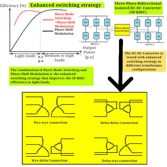
2.1. Wye-Wye (Yy) Connection

Figure 2a shows the Yy connection at the HVS and LVS of the HF transformer, which is a typical transformer configuration for the 3P-BIDC in Figure 1. The power transfer equation for the 3P-BIDC in Yy connection for the phase-shift angle range of 0 δ π 3 is,
P o = P Yy = V 1 N V 2 2 π f s L Yy δ ( 2 3 δ 2 π ) ,
where V1 and V2 are the HVS and LVS DC-link voltages, respectively, fs is the continuous switching frequency, δ is the phase-shift angle between the ac phase voltages of bridges 1 and 2 in radians, N is the transformer turns ratio, and LYy is the per phase leakage inductance of the transformer in the Yy connection.

2.2. Wye-Delta (Yd) and Delta-Wye (Dy) Connection

Figure 2b presents the three-phase transformer in Yd connection. The HVS of the transformer is connected in wye (Y) and the LVS of the transformer is connected in delta (d). The power transfer equation for phase-shift angles in the range of 0 δ π 3 is,
P o = P Yd = V 1 N V 2 2 π f s L Yd ( δ π 6 )
Figure 2c presents the three-phase transformer in Dy connection. This connection is simply the Yd connection operated in reversed direction. The LVS of the transformer is connected in delta (D) and the HVS of the transformer is connected in wye (y). The power transfer equation for phase-shift angles in the range of π 3 δ 0 is,
P o = P D y = V 1 N V 2 2 π f s L Dy ( δ + π 6 )
Since that the transformer configuration of Dy is the Yd configuration in reverse, the phase angle is also the opposite of Yd. The leakage inductance of the 3P-BIDC in Yd and Dy connection designed to operate in buck and boost mode is calculated in Equations (4) and (5) as,
L Yd = L Y + N 2 L d
L Dy = N 2 L D + L y
According to [15,16], the 3P-BIDC can operate under soft-switching mode when the DC-link voltage ratio x is in the range of 3 2 x 2 and 1 2 x 2 3 for Dy and Yd configurations, respectively.

2.3. Delta-Delta (Dd) Connection

Figure 2d presents the three-phase transformer in Dd connection. Both the primary and secondary side of the transformer are connected in delta connection. The phase shift equation is shown in Equation (6) for phase-shift angles of 0 δ π 3 as,
P o = P Dd = V 1 N V 2 2 π f s L Dd δ ( 2 3 δ 2 π )
The leakage inductance, LDd of the 3P-BIDC is equal to LYy. The 3P-BIDC in Dd connection is designed to operate with a DC voltage ratio of 1:1.

3. 3P-BIDC Simulation Model and Burst-Mode Strategy

In light-load conditions, the converter is operated in such a way that the PSM is combined with burst-mode switching to generate an intermittent power transfer. In medium to high-load conditions, only the PSM is employed. The PSM strategy is a continuous switching operation of the 3P-BIDC, while the combination of PSM and burst-mode switching results in intermittent operation of the 3P-BIDC in light-load condition.
Figure 3 presents the theory of generating the burst-mode signals. Note that m is the conducting period and n is the non-conducting period of the burst-mode signal in percentage. The burst-mode strategy is generated by multiplying two signals. The continuous signal of 20 kHz is multiplied with a low frequency signal of 20 Hz. The product is an intermittent signal with a low frequency of 20 Hz. If a 50 ms low frequency signal with a duty cycle of 30% is multiplied with a train of a 50 μs signal of duty cycle 50% each, 300 gate pulses with a period of 50 μs and duty cycle 50% will last for 15 ms and there will be no gate pulses for 35 ms, the average output power will be reduced.
Figure 4 presents the last two cycles of gating signals for T11 and T21 that are transitioning from the conducting period to the non-conducting period. The gating signals have a switching frequency of 20 kHz and are phase-shifted by π/6. The burst mode signal in red has a frequency of 20 Hz. Therefore, T11 and T21 will be switching at 20 kHz when the burst mode signal is in the high state. The intermittent operation is applied for power transfer less than 0.44 p.u. of the rated power.
The phase-shift angle ranges from 0 to π/6 for power transfer from zero to the rated power using continuous operation. Moreover, with the same phase-shift angle, when intermittent operation is applied, the average DC output power is reduced.
Figure 5 shows the simulation model of the 3P-BIDC connected to a battery bank. The HF transformer is varied according to Figure 2. The simulation model considers losses such as copper and switching losses in order to represent a practical converter. The battery is modelled with an internal resistance, Rint, of 5 mΩ. A resistor Rs is connected in series with the transformer to represent copper loss in the transformer windings. On-state collector-emitter voltage of 1.85 V and forward voltage drop of 2.17 V are considered in the IGBTs and diodes, respectively. The IGBT model number is SKM75GB12V with maximum voltage and continuous current ratings of 1.2 kV and 114 A, respectively.
Table 1 shows the 3P-BIDC simulation model parameters. Each design differs in the value of the DC-link voltages, range of phase-shift angle, and the leakage inductances. When the converter is operated in Yd or Dy, the DC-link voltage supply that is connected to the wye side of the transformer is supplied with 520 V and the DC-link voltage that is connected to the delta side of the transformer is supplied with 300 V. This is to allow the 3P-BIDC to operate in buck and boost mode respectively. The rated power of 3 kW is designed to be achieved at δ = π/6 for Yy and Dd connections. On the other hand, the rated power of 3 kW is achieved at δ = π/3 for Yd and at δ = 0 for Dy connections.
Considering the power transfer from bridge 1 to 2, the input (Pi) and output (Po) power are calculated as,
P i = V 1 I 1
and
P o = V 2 I 2
where I1 and I2 are the average current at bridges 1 and 2, respectively. The efficiency of the DC-DC converter is determined as the ratio of the input and output power. Note that, when the power is transferred from bridge 2 to 1, Equations (7) and (8) can be interchanged.

4. 3P-BIDC Simulation Results

4.1. Operating Waveforms

This section presents the results obtained from the simulation of the 3P-BIDC model with different transformer configurations operated in continuous and intermittent switching, in the PSCAD environment. Table 2 presents the DC-link voltage at bridges 1 and 2 with different transformer connections.
Figure 6a–d shows the AC voltage and current waveforms of phase A in bridges 1 and 2 in Yy, Yd, Dy, and Dd transformer connections when the 3P-BIDC is operated using PSM at the rated power. In Figure 6a, the voltage levels of 200 V and 100 V at bridges 1 and 2 correspond to v ap = v as = 2 3 V 1 and v ap = v as = 1 3 V 1 in Yy transformer configuration. AC root mean square (RMS) current of 10 A flows in both the primary and secondary sides of the transformer. In Figure 6b, the voltage values of 347 V and 173 V at bridge 1 correspond to v ap = 2 3 V 1 and v ap = 1 3 V 1 , respectively. The voltage value of 300 V at bridge 2 corresponds to v AB = V 2 . The peak AC current of 5.2 A is seen on the HVS, which is within the rated current of the converter. For the Dy connection, at the rated power of 3 kW, the voltage value of 300 V at bridge 1 corresponds to v ab = V 1 . The voltage values of 347 V and 173 V at bridge 2 correspond to v as = 2 3 V 2 and v as = 1 3 V 2 , respectively. This results in a peak AC current value of 6.6 A at HVS, well within the rated current. The DC-link voltage ratios are 0.58 and 1.73 when the transformer is connected in Yd and Dy configurations, respectively. In Figure 6d, the voltage levels of 520 V at both bridges 1 and 2 correspond to v ab = V 1 and v AB = V 2 .
Figure 7a shows the AC voltage waveform of the 3P-BIDC in Yy transformer configuration for a full cycle of burst-mode with the conducting period of m = 30% and the non-conducting conducting period of n = 70% at δ = π 6 . Figure 7b shows the time-expanded waveform of Figure 7a from the final conducting period to the non-conducting period. During the non-conducting period, AC voltage shows a time decaying oscillation with the maximum voltage of 50 V and the rms voltage of 35.4 V.

4.2. Efficiency in Various Transformer Configurations

This section presents the light-load efficiency performance of the 3P-BIDC. The efficiency improvement that compares between continuous and intermittent mode is observed and evaluated at light-loads of 0.12 p.u. and 0.24 p.u. of the rated power.
Figure 8 presents the relationship between the phase-shift angles of π 3 δ π 3 and the output power between ±1 per unit, for charging and discharging power. It can be seen that the phase-shift angle required to achieve the output power from 0 to 1 p.u. changes with different transformer connections. The power is transferred from primary side to secondary side in Yy and Dd transformer connections when 0 δ π 6 . The rated power is achieved at δ = π 6 . In Yd and Dy configurations, the power is transferred from the primary side to the secondary side when π 6 δ π 3 and π 6 δ 0 , respectively.
Figure 9 presents the efficiency versus output power curve of the 3P-BIDC with various transformer configurations in the continuous operation. The 3P-BIDC in Yd configuration achieved higher efficiency below 0.28 p.u. and above 0.81 p.u. of the rated power as compared to the other transformer configurations. The figure also shows that at 0.12 p.u. the efficiency of 3P-BIDC in Yy configuration is 83.6% and in Yd configuration it is 89.4%. Moreover, at 0.20 p.u., the efficiency of the 3P-BIDC in Yy configuration is 90% and in Yd configuration it is 93%. There is a significant drop in efficiency in the 3P-BIDC during light-load operation (<0.3 p.u.) for all transformer configurations. The 3P-BIDC has poor efficiency when connected to the Dy transformer.
Figure 10 presents the improvement in 3P-BIDC efficiency of different transformer configurations when intermittent switching is employed. Figure 10a shows that when the 3P-BIDC is connected in Yy or Dd transformer configuration, higher efficiency is achieved with m = 30 % compared to m = 10 % from power 0.12 p.u. to 0.3 p.u. in terms of improving the converter efficiency. An efficiency as high as 99.6% is achieved at the power transfer of 0.29 p.u when intermittent operation is employed with m = 30 % . Figure 10b shows that in Yd transformer configuration, the 3P-BIDC efficiency using intermittent switching with m = 10 % is higher compared to m = 30 % from power transfer of 0.12 p.u. to 0.21 p.u. For example, at the power transfer of 0.16 p.u., the efficiency of the 3P-BIDC with intermittent switching m = 10 % is 96%, whereas the efficiency of the 3P-BIDC with m = 30 % is 94.1%. At the power transfer of 0.22 p.u., it is seen that the efficiency of the 3P-BIDC with m = 30 % outperforms the efficiency of the 3P-BIDC with m = 10 % . At the power transfer of 0.29 p.u., the efficiency of the 3P-BIDC with m = 10 % is 95.7%, whereas the efficiency of the 3P-BIDC with m = 30 % is 97%. Figure 10c shows that the 3P-BIDC in Dy transformer winding configuration obtained higher efficiency improvements with m = 10 % at the power transfer of 0.03 p.u. to 0.25 p.u. For example, at the power transfer of 0.18 p.u., the efficiency of the 3P-BIDC with m = 10 % is 90.3%. At the power transfer of 0.25 p.u., m = 10% reached the maximum range of δ = π 3 and the intermittent switching is operated with m = 30 % . The overall efficiency of the DC-DC converter in Dy transformer configuration is low compared to the efficiency performance of the DC-DC converter in Yy, Dd, and Yd transformer configurations, which are above 95% in the light-load conditions. The authors of [6] showed that no improvement in efficiency of the 3P-BIDC is achieved when the converter is operated in intermittent switching for medium load. However, the simulation results in Figure 10 show that the efficiency of the 3P-BIDC significantly improved during light-load operation with intermittent switching. Therefore, the intermittent switching is suitable for light-load operation of the 3P-BIDC.
Table 3 and Table 4 summarizes the efficiency improvement and power loss reduction of the 3P-BIDC with Yy, Yd, Dy, and Dd transformer configurations that are observed at light-load power transfers of 0.12 p.u., 0.24 p.u., and 0.29 p.u, accordingly. As shown in Table 3, the efficiency improvements of the 3P-BIDC achieved in Yy and Dd transformer configurations at light-load power transfers of 0.12 p.u, 0.24 p.u, and 0.29 p.u are higher compared to the efficiency improvement achieved in Yd transformer configuration. The DC-DC converter in Dy transformer configuration achieved high efficiency improvements. However, the overall efficiency remained below 95% in intermittent switching. Table 4 is consistent in showing that the DC-DC converter achieved the highest power loss reduction in Dy transformer configuration at light loads. However, the power loss of the DC-DC converter in Dy transformer configuration when in intermittent operation is higher than the power losses of the DC-DC converter in Yy, Dd, and Yd transformer configurations.
The 3P-BIDC has the best performance when operated with Yy and Dd transformer configuration with a DC voltage ratio that is equal to the transformer turns ratio. The Yd transformer configuration may also be suitable for applications with different DC voltage ratios such as 520 V and 300 V. On the other hand, the Dy transformer configuration is unfavorable due to the efficiency achievements of lower than 95% despite intermittent switching being applied. Note that this paper has not observed the efficiency performance of the 3P-BIDC when the DC voltage ratio of the 3P-BIDC is not the same as the transformer turns ratio.

4.3. Analysis of Current Stress in Transformer and IGBT Switches

A stress analysis was conducted on the modelled three-phase transformer and switches to compare the amount of current stresses on each of the different transformer configurations with the turns ratio of 1:1. This section theoretically analyses the current stress in the transformer and switches of 3P-BIDC in different transformer configurations, based on the method in [15]. This theoretical analysis is then compared with the simulation results.
Table 5 shows the equations used to theoretically calculate the transformer rms current and the switch rms and transient currents in the 3P-BIDC in the various transformer configurations. The variable d represents the voltage conversion ratio. In this analysis, d is always equal to 1. This shows that the voltage conversion ratio is equal to the transformer turns ratio in all transformer configurations.
Figure 11 presents the different current stresses in the transformers and switches versus the output average current of the 3P-BIDC in per unit terms based on the converter rated current. In Yy, Dd, and Dy, the base current is 10 A and in Yd, the base current is 6 A. The base current is multiplied by 2 for analysis that involves summation of currents in both sides of the converter.
This analysis is conducted for the power transfer range of 0 to the rated power, where the average current at the DC side ranges between 0 and 1 p.u. Figure 11a shows the rms phase current of the transformer. It is shown that the current stress increases significantly with the output average current in Dd transformer configuration. It exceeds the rated current at the output average current of 0.76 p.u. Figure 11b shows the summation of the rms current of one phase in bridges 1 and 2, which is used to determine the conduction current stress on the semiconductor switches. The rms current stress of the switches exceeds 1 p.u. from very low output current for Yd, and from output current of 0.42 p.u. for Dd transformer configurations.
The Yy transformer configuration results in lowest conduction current stress on the switches. Figure 11c shows the summation of the current of one phase in bridges 1 and 2 during a switching instant. The Yd and Dy transformer configurations are the least sensitive to the changes in output average current. However, the rms current stresses in the transient modes of the 3P-BIDC in Yd, Dy, and Dd transformer configurations exceed 1 p.u. for all output current range, which indicates high switching current stress for those transformer configurations. The switching current stress in Yy transformer configuration is the lowest of all the four types of transformer configurations and does not exceed the rated current except only after 0.82 p.u. of average output current. Therefore, it can be seen that the Yy transformer configuration is most suitable for 3P-BIDC in terms of low current stress when d is 1.
where
r 1 = π 3 ( 5 d 2 10 d + 5 ) + d ( 27 δ 3 ) + 54 δ 2 π ,   p 1 = | 2 π + d ( 3 δ 2 π ) | + | 3 δ + 2 π ( d 1 ) | ,
m 1 = π 2 ( 15 d 2 15 d + 5 ) + d ( 81 δ 2 27 δ π ) ,   g 1 = π ( | d 2 3 | + | 2 d 1 | ) ,
j 1 = π 2 ( 5 d 2 15 d + 15 ) + d ( 81 δ 2 + 27 δ π ) ,   q 1 = π ( | d 2 | + | 2 d 3 1 | ) .
Figure 12 presents the comparison of the theoretical analysis and the simulated analysis of the 3P-BIDC in Yy transformer configuration. In Figure 12a, the stress analysis in the rms current of the transformer in the simulation differs only by 1% to the theoretical results. Figure 12b shows that the highest error percentage of the analysis is 8% by comparing the summation of the rms currents in the switches that corresponds to one phase of bridges 1 and 2.

5. Power Loss Estimation

This section presents the estimated power loss distribution and calculation details of the 3P-BIDC at light-load conditions of 0.12 p.u. and 0.34 p.u. of the rated power in the continuous mode of operation and comparing it with the light-load conditions of 0.12 p.u. and 0.34 p.u. of the rated power with a Yy transformer connection. The types of losses considered in the simulation model are copper losses, conduction losses, and snubber losses. Note that snubber losses are not considered in the power loss calculations in intermittent operation.

5.1. Distribution of Losses

5.1.1. Copper Loss

The transformer winding resistance is modelled as 15 mΩ in each phase of the transformer. The winding resistance give rise to practical copper loss in the windings of the transformer. The total copper loss is calculated as,
P cu = 3 [ I 1 2 R 1 + I 2 2 R 2 ]
The rms current across the LVS, I1 and the rated current across the HVS, I2 at 0.12 p.u is 1.2 A. Therefore, the total copper loss is 0.13 W.

5.1.2. Conduction Loss

Conduction loss includes loss during the conduction of an IGBT and a diode of the model SKM75GB12V. In every switching cycle, only three switches and three diodes conduct. The conduction loss of the 3P-BIDC is calculated as,
P c o n d = 3 ( V CE + V F ) ( I avg )
where VCE is the on-state collector-emitter voltage of the conducting IGBT, VF is the forward voltage drop of the conducting diode, and Iavg is the average current.

5.1.3. Snubber Loss

The 3P-BIDC is assumed to have snubber loss if zero-voltage switching (ZVS) is not achieved. The snubber loss is calculated as,
P snub = X C s V 2 2 f s
where X is the number of switches that is involved in snubber loss and V2 is the DC-link voltage at the secondary side.
The converter operated at 0.12 p.u. is assumed to have hard-switching in bridge 1. Therefore, the number of switches that experience snubber loss, X, is 6. Since ZVS occurs at 0.34 p.u., the snubber loss is neglected.

5.1.4. Switching Loss

In practical conditions, the turn-off switching loss is not negligible. If ZVS turn on is achieved, turn-on switching loss is negligible. The average turn-off switching loss is directly proportional to the square of the switching current and the switch current fall time [29],
P SW = T f 48 C s I SW 2
where I SW is the turn-off switching current and T f is the switching current fall time. However, in the simulation, only on-state voltage drop and diode forward voltage drop are considered. Therefore, T f is very short, rendering the switching loss negligible.

5.1.5. Total Power Loss

The total power loss PLoss in the 3P-BIDC is calculated as the summation of copper Pcu, conduction Pcond, and snubber Psnub losses,
P Loss = P cu + P cond + P snub
The total estimated power loss at 0.12 p.u. and 0.34 p.u. at the rated power is 74.7 W (0.025 p.u.) and 25.3 W (0.008 p.u.), respectively.

5.2. Numerical Calculation of Losses

This sub-section provides the numerical calculation of losses in the 3P-BIDC at the power transfer of 0.12 p.u. and 0.34 p.u. at the rated voltage. The power loss is calculated when only PSM and intermittent operation are employed. From Figure 10, it can be seen that the onset of ZVS is around 0.34 p.u. of power transfer. Hence, no snubber loss is accounted for at the power transfer of 0.34 p.u.

5.2.1. Power Loss at 0.12 p.u (δ = 4°) in Continuous Mode

  • Copper loss
P cu = 3 [ I 1 2 R 1 + I 2 2 R 2 ] P cu = 3 [ 1.2 2 ( 0.015 ) + 1.2 2 ( 0.015 ) ] = 0.13   W   ( 0.000043   p . u . )
  • Conduction loss
P cond = 3 ( V CE + V F ) ( I avg ) P cond = 3 ( 1.85 + 2.17 ) ( 0.816 ) = 9.8   W   ( 0.0033   p . u . )
  • Snubber loss
P snub =   X C s V b 2 f s P snub = ( 6 ) ( 6 × 10 9 ) ( 300 ) 2 ( 20 × 10 3 ) = 64.8   W   ( 0.0216   p . u . ) P Loss = P cu + P cond + P snub = 0.13   W + 9.8   W + 64.8   W = 74.73   W   ( 0.025   p . u . )

5.2.2. Power Loss at 0.34 p.u. (δ = 10°) in Continuous Mode

  • Copper loss
P cu = 3 [ I 1 2 R 1 + I 2 2 R 2 ] P cu = 3 [ 3.63 2 ( 0.015 ) + 3.63 2 ( 0.015 ) ] = 1.19   W   ( 0.0004   p . u . )
  • Conduction loss
P cond = 3 ( V CE + V F ) ( I avg ) P cond = 3 ( 1.85 + 2.17 ) ( 2 ) = 24.12   W   ( 0.008   p . u . ) P Loss = P cu + P cond + P snub = 1.19   W   + 24.12   W   + 0   W = 25.31   W   ( 0.008   p . u . )
The losses in intermittent operation are calculated with the same equation as in continuous operation. However, since that this intermittent operation is carried out with m = 30%, the calculated total power loss is multiplied by a factor of 0.3. The phase-shift angles to achieve the power transfer 0.12 p.u. and 0.34 p.u. in the intermittent operation are higher than when only continuous operation is employed.

5.2.3. Power Loss at 0.12 p.u. (δ = 7°) in Intermittent Mode

  • Copper loss
P cu = 3 [ I 1 2 R 1 + I 2 2 R 2 ] P cu = 3 [ 1.18 2 ( 0.015 ) + 1.18 2 ( 0.015 ) ] = 0.125   W   ( 0.000042   p . u . )
  • Conduction loss
P cond = 3 ( V CE + V F ) ( I avg ) P cond = 3 ( 1.85 + 2.17 ) ( 1.4 ) = 16.9   W   ( 0.006   p . u . )
  • Snubber loss
P snub = X C s V b 2 f s P snub = ( 6 ) ( 6 × 10 9 ) ( 300 ) 2 ( 20 × 10 3 ) = 64.8   W   ( 0.0216   p . u . ) P Loss = P cu + P cond + P snub = 0.13   W   + 9.8   W   + 64.8   W = 74.73   W   ( 0.025   p . u )   P Loss = 0.3 [ P cu + P cond + P snub ] = 0.3 [ 1.125   W   + 16.9   W   + 64.8   W ] = 24.5   W   ( 0.008   p . u . )

5.2.4. Power Loss at 0.34 p.u. (δ = 19°) in Intermittent Mode

  • Copper loss
P cu = 3 [ I 1 2 R 1 + I 2 2 R 2 ] P cu = 3 [ 4.9 2 ( 0.015 ) + 4.9 2 ( 0.015 ) ] = 2.16   W   ( 0.00072   p . u . )
  • Conduction loss
P cond = 3 ( V CE + V F ) ( I avg ) P cond = 3 ( 1.85 + 2.17 ) ( 2.8 ) = 33.8   W   ( 0.0071   p . u . ) P Loss = 0.3 [ P cu + P cond + P snub ] = 0.3 [ 2.16   W + 33.8   W + 0   W ] = 10.77   W   ( 0.004   p . u . )
Considering the Yy transformer winding configuration, Figure 13 presents the calculated total loss, compared with the total loss measured from the simulation model, in continuous and intermittent mode of operations focusing on the power levels 0.12 p.u. to 0.34 p.u. The figure shows that the minimum power loss is obtained at the power transfer of 1.02 kW, which also indicates the onset of ZVS [19], hence snubber loss can be negligible.
Figure 14a,b presents the copper, conduction, and snubber losses in per unit terms in the continuous mode of operation. The copper loss increases as the output power increases. This is because there is a higher rated current flow through the transformer, resulting in higher I2R losses.
Figure 15a,b presents the copper and conduction per unit losses in intermittent operation. It is shown that the intermittent operation applied at 0.12 p.u. and 0.34 p.u. reduced the amount of losses by 3–4%. This is because the number of switching cycles are reduced, therefore reducing the total losses in the output.

6. Conclusions

This paper presented the operational feasibility and efficiency performance evaluation of the 3 kW 3P-BIDC in Yy, Yd, Dy, or Dd transformer winding configuration using the combination of PSM and burst-mode switching to improve the low power transfer efficiency of the converter. The 3P-BIDC achieved the highest efficiency performance in Yy and Dd transformer configurations in light-load power transfers in intermittent operation. However, the Yd transformer configuration is suitable and can result in high efficiency when the DC voltage is not equal on either side of the 3P-BIDC. It is not preferred to operate the 3P-BIDC with a Dy transformer connection as it results in the overall poorest 3P-BIDC efficiency performance amongst the other transformer configurations. The theoretical current stress analysis shows that the 3P-BIDC operated with Yy transformer configuration results in the lowest current stress in the transformer and switches. Moreover, the loss analysis is comparable to the stress and loss measured in the simulation model for the 3P-BIDC in Yy transformer configuration.

Author Contributions

Conceptualization, N.M.L.T.; methodology, N.S.M.S. and N.M.L.T.; simulation, N.S.M.S.; validation, N.S.M.S., N.M.L.T. and H.A.; formal analysis, N.S.M.S. and N.M.L.T.; investigation, N.S.M.S.; resources, N.S.M.S. and N.M.L.T.; data curation, N.S.M.S.; writing—original draft preparation, N.S.M.S. and N.M.L.T.; writing—review and editing, N.S.M.S., N.T. and H.A.; visualization, N.M.L.T.; supervision, N.M.L.T.; project administration, N.M.L.T.; funding acquisition, N.M.L.T. All authors have read and agreed to the published version of the manuscript.

Funding

This research was financially supported by the Ministry of Higher Education through FRGS Project No. FRGS/1/2017/TK04/UNITEN/02/4. The APC was supported by UNITEN BOLD Publication Fund.

Conflicts of Interest

The authors declare no conflict of interest.

References

  1. De Doncker, R.W.A.A.; Divan, D.M.; Kheraluwala, M.H. A Three-Phase Soft-Switched High-Power-Density DC/DC Converter for High-Power Applications. IEEE Trans. Ind. Appl. 1991, 27, 63–73. [Google Scholar] [CrossRef]
  2. Tan, N.M.L.; Inoue, S.; Kobayashi, A.; Akagi, H. An energy storage system combining a 320-V, 12-F electric double layer capacitor bank with a bidirectional isolated DC-DC converter. IEEE Trans. Power Electron. 2008, 23, 2755–2765. [Google Scholar] [CrossRef]
  3. Nguyen, D.D.; Bui, N.T.; Yukita, K. Design and optimization of three-phase dual-active-bridge converters for electric vehicle charging stations. Energies 2019, 13, 150. [Google Scholar] [CrossRef] [Green Version]
  4. Lei, T.; Wu, C.; Liu, X. Multi-objective optimization control for the aerospace dual-active bridge power converter. Energies 2018, 11, 1168. [Google Scholar] [CrossRef] [Green Version]
  5. Tan, N.M.L.; Abe, T.; Akagi, H. Design and performance of a bidirectional isolated DC-DC converter for a battery energy storage system. IEEE Trans. Power Electron. 2012, 27, 1237–1248. [Google Scholar] [CrossRef]
  6. Baars, N.H.; Everts, J.; Huisman, H.; Duarte, J.L.; Lomonova, E.A. A 80-kW Isolated DC–DC Converter for Railway Applications. IEEE Trans. Power Electron. 2015, 30, 6639–6647. [Google Scholar] [CrossRef]
  7. De Din, E.; Siddique, H.A.B.; Cupelli, M.; Monti, A.; De Doncker, R.W. Voltage Control of Parallel-Connected Dual-Active Bridge Converters for Shipboard Applications. IEEE J. Emerg. Sel. Top. Power Electron. 2018, 6, 664–673. [Google Scholar] [CrossRef]
  8. Saeed, M.; Rogina, M.R.; Rodríguez, A.; Arias, M.; Briz, F. SiC-Based High Efficiency High Isolation Dual Active Bridge Converter for a Power Electronic Transformer. Energies 2020, 13, 1198. [Google Scholar] [CrossRef] [Green Version]
  9. Sathishkumar, P.; Krishna, T.N.; Khan, M.A.; Zeb, K.; Kim, H.-J. Digital Soft Start Implementation for Minimizing Start-Up Transients in High Power DAB-IBDC Converter. Energies 2018, 11, 956. [Google Scholar] [CrossRef] [Green Version]
  10. Calderon, C.; Barrado, A.; Rodriguez, A.; Alou, P.; Lazaro, A.; Fernandez, C.; Zumel, P. General Analysis of Switching Modes in a Dual Active Bridge with Triple Phase Shift Modulation. Energies 2018, 11, 2419. [Google Scholar] [CrossRef] [Green Version]
  11. Krismer, F.; Kolar, J.W. Closed form solution for minimum conduction loss modulation of DAB converters. IEEE Trans. Power Electron. 2012, 27, 174–188. [Google Scholar] [CrossRef]
  12. Everts, J. Closed-Form Solution for Efficient ZVS Modulation of DAB Converters. IEEE Trans. Power Electron. 2017, 32, 7561–7576. [Google Scholar] [CrossRef]
  13. Oggier, G.G.; Ordonez, M. High-efficiency DAB converter using switching sequences and burst mode. IEEE Trans. Power Electron. 2016, 31, 2069–2082. [Google Scholar] [CrossRef]
  14. Yan, G.; Li, Y.; Jia, Q. Comparative Analysis of Single and Three-phase Dual Active Bridge Bidirectional DC-DC Converter Based on the Phase-Shifting Control. In Proceedings of the 2016 International Conference on Energy, Power and Electrical Engineering (EPEE 2016), Shenzhen, China, 30–31 October 2016; pp. 326–333. [Google Scholar]
  15. Núñez, R.O.; Oggier, G.G.; Botterón, F.; García, G.O. A comparative study of Three–Phase Dual Active Bridge Converters for renewable energy applications. Sustain. Energy Technol. Assess. 2017, 23, 1–10. [Google Scholar] [CrossRef]
  16. Baars, N.H.; Everts, J.; Wijnands, C.G.E.; Lomonova, E.A. Performance Evaluation of a Three-Phase Dual Active Bridge DC-DC Converter with Different Transformer Winding Configurations. IEEE Trans. Power Electron. 2016, 31, 6814–6823. [Google Scholar] [CrossRef]
  17. Sharifuddin, N.S.M.; Tan, N.M.L.; Akagi, H. Low-load Efficiency Improvement of a Three-Phase Bidirectional Isolated DC-DC Converter (3P-BIDC) Via Enhanced Switching Strategy. Int. J. Eng. Technol. 2018, 7, 932–938. [Google Scholar] [CrossRef]
  18. Van Hoek, H.; Jacobs, K.; Neubert, M.; De Doncker, R.W. Enhanced operating strategy for a three-phase dual-active-bridge converter including frequency variation. In Proceedings of the 2015 IEEE 11th International Conference on Power Electronics and Drive Systems, Sydney, Australia, 9–12 June 2015; pp. 492–498. [Google Scholar]
  19. Choi, H.J.; Jung, S.H.; Jung, J.H. A Novel Switching Algorithm to improve Efficiency at light load conditions for Three-Phase DAB Converter in LVDC Application. In Proceedings of the 2018 International Power Electronics Conference (IPEC-Niigata 2018-ECCE Asia), Niigata, Japan, 20–24 May 2018; pp. 383–387. [Google Scholar]
  20. Haneda, R.; Akagi, H. Design and Performance of the 850-V 100-kW 16-kHz Bidirectional Isolated DC-DC Converter Using SiC-MOSFET/SBD H-Bridge Modules. IEEE Trans. Power Electron. 2020. Early Access. [Google Scholar] [CrossRef]
  21. Tan, Z.Y.; Tan, N.M.L.; Hussain, I.S. Theoretical Analysis of a Three-Phase Bidirectional Isolated DC-DC Converter Using Phase-Shifted Modulation. Int. J. Power Electron. Drive Syst. 2018, 9, 495–503. [Google Scholar] [CrossRef]
  22. Engel, S.P.; Soltau, N.; Stagge, H.; De Doncker, H. Dynamic and balanced control of three-phase high-power dual-active bridge DC-DC converters in DC-grid applications. IEEE Trans. Power Electron. 2013, 28, 1880–1889. [Google Scholar] [CrossRef]
  23. Wang, B.; Xiaoni, X.; Wu, S.; Wu, H.; and Ying, J. Analysis and implementation of LLC burst mode for light load efficiency improvement. In Proceedings of the 2009 Twenty-Fourth Annual IEEE Applied Power Electronics Conference and Exposition, Washington, DC, USA, 15–19 February 2009; pp. 58–64. [Google Scholar]
  24. Reverter, F.; Gasulla, M. Optimal Inductor Current in Boost DC/DC Converters Operating in Burst Mode Under Light-Load Conditions. IEEE Trans. Power Electron. 2016, 31, 15–20. [Google Scholar] [CrossRef] [Green Version]
  25. Vasic, D.; Liu, Y.P.; Costa, F.; Schwander, D. Piezoelectric transformer-based DC/DC converter with improved burst-mode control. In Proceedings of the 2013 IEEE Energy Conversion Congress and Exposition, Denver, CO, USA, 15–19 September 2013; pp. 147–153. [Google Scholar]
  26. Abramson, R.A.; Gunter, S.J.; Otten, D.M.; Afridi, K.K.; Perreault, D.J. Design and evaluation of a reconfigurable stacked active bridge dc/dc converter for efficient wide load-range operation. In Proceedings of the IEEE Applied Power Electronics Conference and Exposition (APEC), Tampa, FL, USA, 26–30 March 2017; pp. 3391–3401. [Google Scholar]
  27. Trescases, O.; Wen, Y. A survey of light-load efficiency improvement techniques for low-power dc-dc converters. In Proceedings of the 8th International Conference on Power Electronics-ECCE Asia, Jeju, Korea, 30 May–3 June 2011; pp. 326–333. [Google Scholar]
  28. Jang, Y.; Jovanovic, M.M.; Dillman, D.L. Light-Load Efficiency Optimization Method. In Proceedings of the Twenty-Fourth Annual IEEE Applied Power Electronics Conference and Exposition (APEC 2009), Washington, DC, USA, 15–19 February 2009; Volume 25, pp. 1138–1144. [Google Scholar]
  29. Akagi, H.; Yamagishi, T.; Tan, N.M.L.; Miyazaki, Y.; Kinouchi, S.I.; Koyama, M. Power-loss breakdown of a 750-V 100-kW 20-kHz bidirectional isolated DC-DC converter using SiC-MOSFET/SBD dual modules. IEEE Trans. Ind. Appl. 2015, 51, 420–428. [Google Scholar] [CrossRef]
Figure 1. A bidirectional isolated DC-DC converter topology.
Energies 13 02836 g001
Figure 2. Types of three-phase transformer configurations. (a) Yy. (b) Yd. (c) Dy. (d) Dd.
Energies 13 02836 g002
Figure 3. Generation of burst-mode signals by multiplying a continuous 20 kHz signal with one cycle of 20 Hz signal with a conduction period, m, of 30%.
Energies 13 02836 g003
Figure 4. Gating signals to switches T11 and T21 at δ = 30° when multiplied with the burst signal.
Energies 13 02836 g004
Figure 5. Simulation model of the three-phase bidirectional isolated DC-DC converter (3P-BIDC) with the Yy transformer connection.
Energies 13 02836 g005
Figure 6. AC voltage and current waveforms of the 3P-BIDC in different transformer configurations operating in phase-shift modulation (PSM) at the rated power. (a) Yy. (b) Yd. (c) Dy. (d) Dd.
Energies 13 02836 g006
Figure 7. AC voltage waveform of the 3P-BIDC in Yy transformer connection using burst-mode. (a) At δ = π/6. (b) Time-expanded waveform of (a).
Energies 13 02836 g007
Figure 8. Phase-shift angle versus output power curve of the 3P-BIDC with different transformer configurations.
Energies 13 02836 g008
Figure 9. Efficiency versus output power curve of the 3P-BIDC with different transformer configurations in continuous operation.
Energies 13 02836 g009
Figure 10. Efficiency versus output power curve of the 3P-BIDC with different transformer configurations in light-load conditions of less than 0.3 p.u. (a) Yy and Dd. (b) Yd. (c) Dy.
Energies 13 02836 g010
Figure 11. Current stresses in 3P-BIDC. (a) Transformer rms phase current. (b) Summation of the rms currents in one phase of bridges 1 and 2. (c) Summation of currents at switching instants in one phase of bridges 1 and 2.
Energies 13 02836 g011
Figure 12. Comparison of theoretical and simulation results of current stress analysis. (a) Transformer rms current. (b) Summation of rms currents in one phase of bridges 1 and 2 of the 3P-BIDC.
Energies 13 02836 g012
Figure 13. Output power versus power loss of the 3P-BIDC in continuous mode and intermittent mode during light-load condition with Yy transformer configuration.
Energies 13 02836 g013
Figure 14. Power loss distribution of the 3P-BIDC in continuous operation; snubber, copper, and conduction losses at (a) 0.12 p.u. (b) 0.34 p.u.
Energies 13 02836 g014
Figure 15. Power loss distribution of the 3P-BIDC in intermittent operation; copper loss and conduction loss at (a) 0.12 p.u. (b) 0.34 p.u.
Energies 13 02836 g015
Table 1. 3P-BIDC Circuit Parameters.
ParametersSymbolValues
Rated PowerPR3 kW
Dc-link voltage at bridge 1V1300 Vu,w
520 Vv
Dc-link voltage at bridge 2V2300 Vu,v
520 Vw
Range of phase-shift angle δ π 3 δ π 3
Switching frequencyfs20 kHz
Dc-link capacitorsC1, C23 mF
Snubber capacitorsC11C266 nF
Transformer turns ratioN:11:1
Transformer leakage inductances/phaseLa, Lb, Lc36.5 μHu (0.15 p.u)
216 μHv (0.31 p.u)
LA, LB, LC36.5 μHu (0.15 p.u)
216 μHw (0.31 p.u)
Transformer winding resistance/phaseRs15 mΩ (0.0005 p.u)
u Applies to Yy and Dd configuration, v Applies to Yd configuration, w Applies to Dy configuration. u Based on 300 V, 3 kW and 20 kHz. v,w Based on 520 V, 3 kW and 20 kHz.
Table 2. DC-link voltages at bridge 1 and bridge 2.
ScenarioDc-Link VoltageTransformer Connection
V1 (V)V2 (V)HVSLVS
1300300WyeWye
2520300WyeDelta
3300520DeltaWye
4300300DeltaDelta
Table 3. Efficiency improvement with continuous and intermittent operation in different transformer configurations.
Po (p.u)Transformer Configurations
Yy and DdYdDy
Efficiency (%)EI (%)Efficiency (%)EI (%)Efficiency (%)EI (%)
ABABAB
0.1283.695.6
(m = 30%)
1289.693.5
(m = 10%)
3.967.087.0
(m = 10%)
20
0.2492.699.2
(m = 30%)
6.694.997.0
(m = 30%)
2.181.890.9
(m = 10%)
9.1
0.2996.099.6
(m = 30%)
3.696.097.3
(m = 30%)
1.387.891.2
(m = 30%)
3.4
A—Continuous mode, B—Intermittent mode, EI (%)—Efficiency improvement as a percentage.
Table 4. Power loss reduction with continuous and intermittent operation in different transformer configurations.
Po (p.u)Transformer Configurations
Yy and DdYdDy
Power Loss (p.u.)PLR (p.u.)Power Loss (p.u.)PLR (p.u.)Power Loss (p.u.)PLR (p.u.)
ABABAB
0.120.0240.006
(m = 30%)
0.0180.0140.010
(m = 10%)
0.0040.0490.02
(m = 10%)
0.029
0.240.0180.002
(m = 30%)
0.0160.0140.008
(m = 30%)
0.0060.0480.02
(m = 10%)
0.028
0.290.0130.001
(m = 30%)
0.0120.0140.008
(m = 30%)
0.0060.0440.03
(m = 30%)
0.014
A—Continuous mode, B—Intermittent mode, PLR (p.u)—Power loss reduction in per unit.
Table 5. Transformers RMS current and switch RMS and transient currents.
Transformer ConfigurationsRange of Phase Shift Angle (rad) I T rms I rms I sw
Yy 0 δ π 3 V 1 243 π ω L Yy r 1 2 V 1 243 π ω L Yy r 1 | 2 V 1 9 ω L Yy | p 1
Yd 0 δ π 3 V 1 243 ω L Yd m 1 ( 3 + 3 ) V 1 27 ω L Yd m 1 | 2 V 1 3 ω L Yd | g 1
Dy π 3 δ 0 V 1 243 π ω L Dy j 1 ( 3 + 3 ) V 1 27 ω L Dy j 1 | 2 V 1 3 ω L Dy | q 1
Dd 0 δ π 3 V 1 9 π ω L Dd r 1 6 V 1 243 π ω L Dd r 1 | 2 V 1 3 ω L Dd | p 1

