Photovoltaic-Driven SiC MOSFET Circuit Breaker with Latching and Current Limiting Capability


Abstract
:1. Introduction
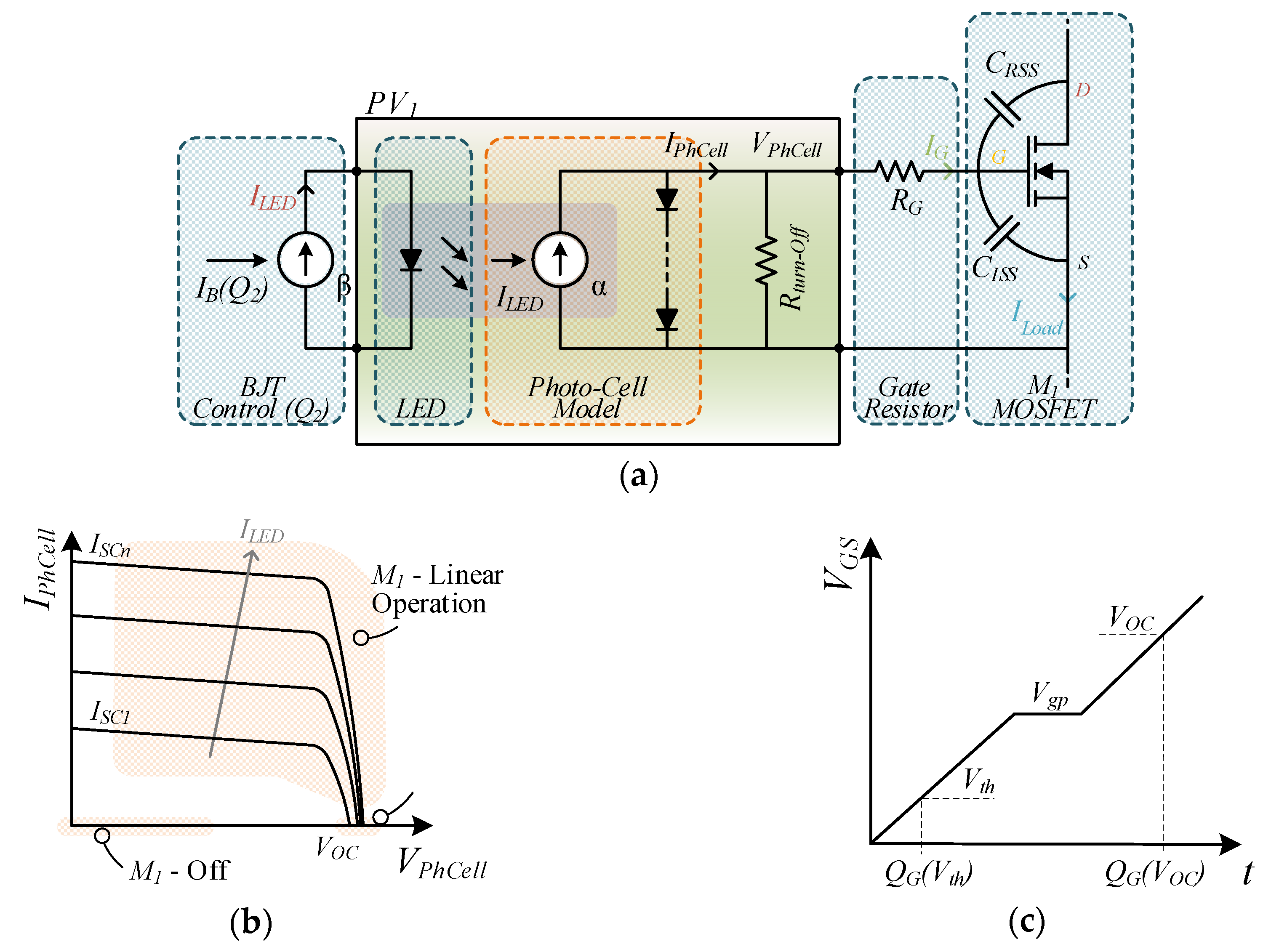
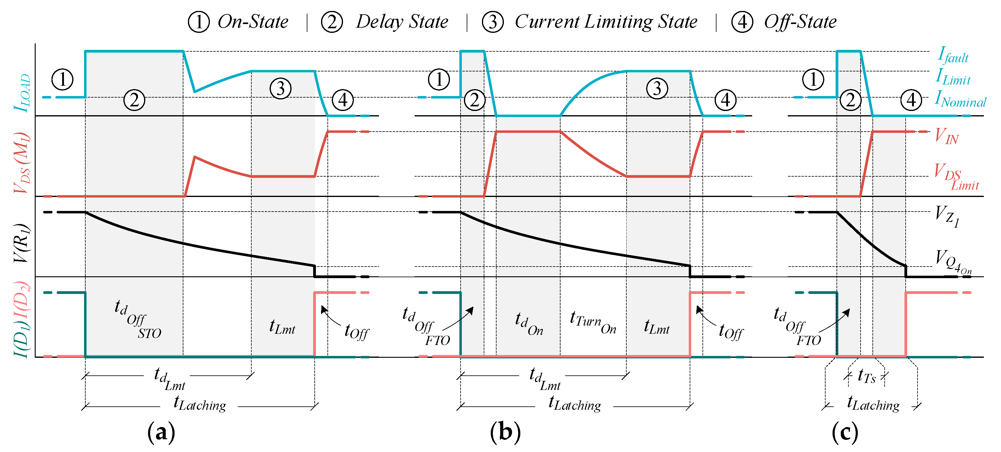
2. SSCB-LCL Description and Operating Principle
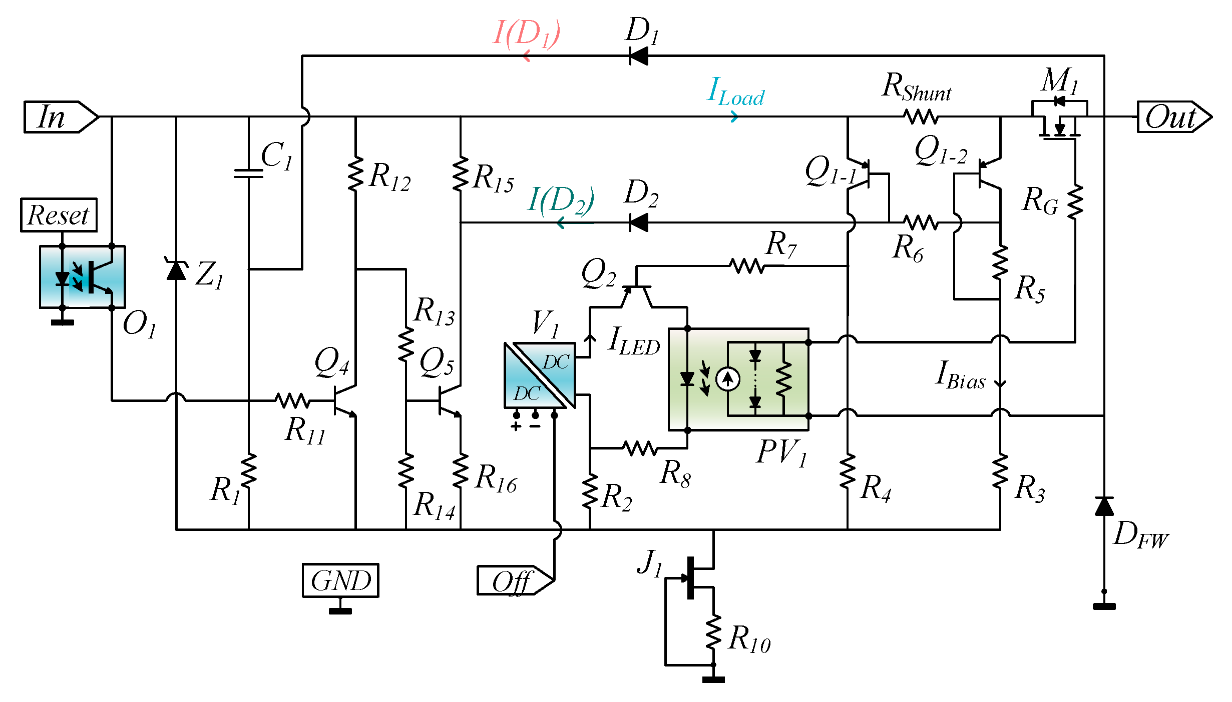
3. SSCB-LCL Circuit Configuration
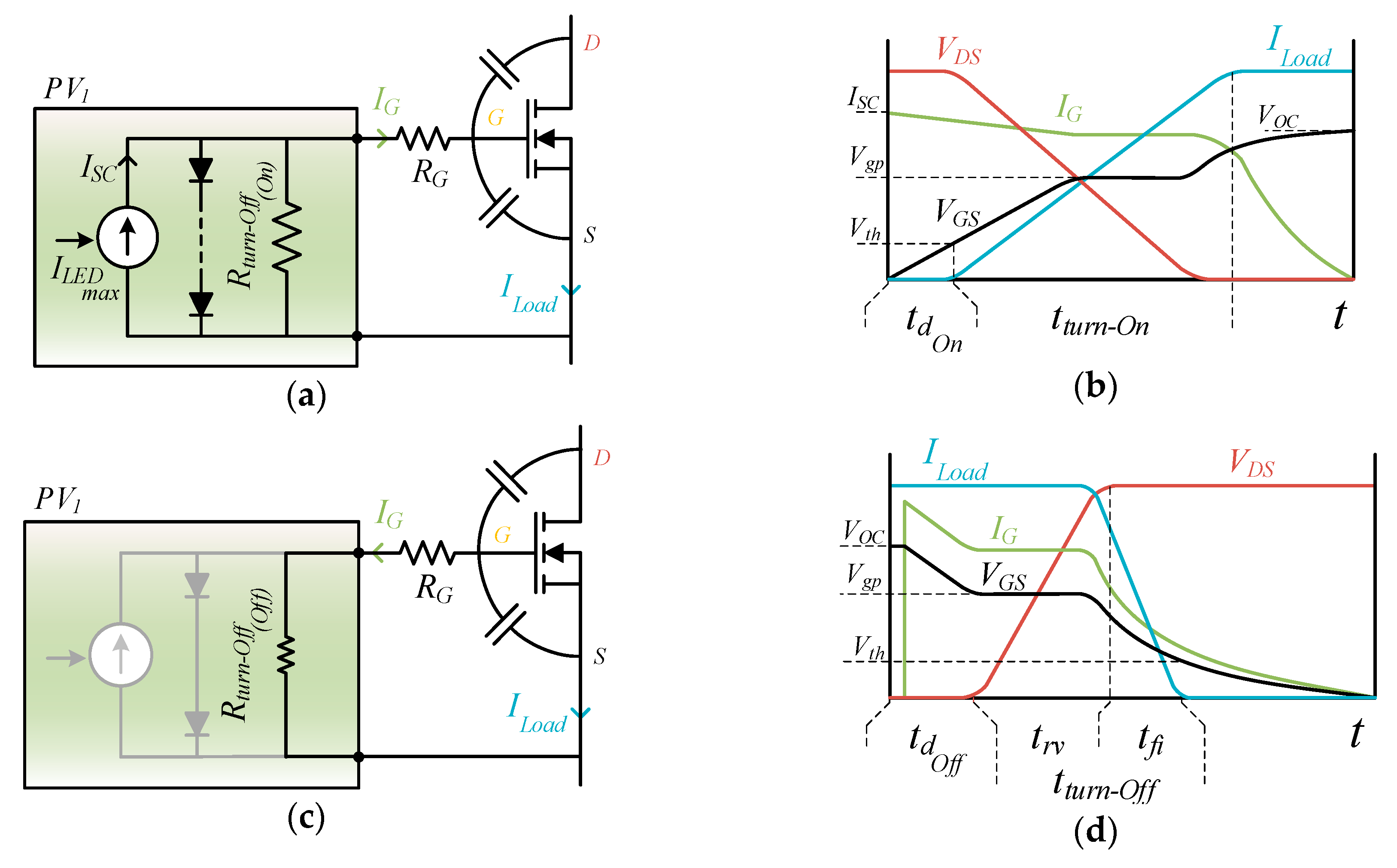
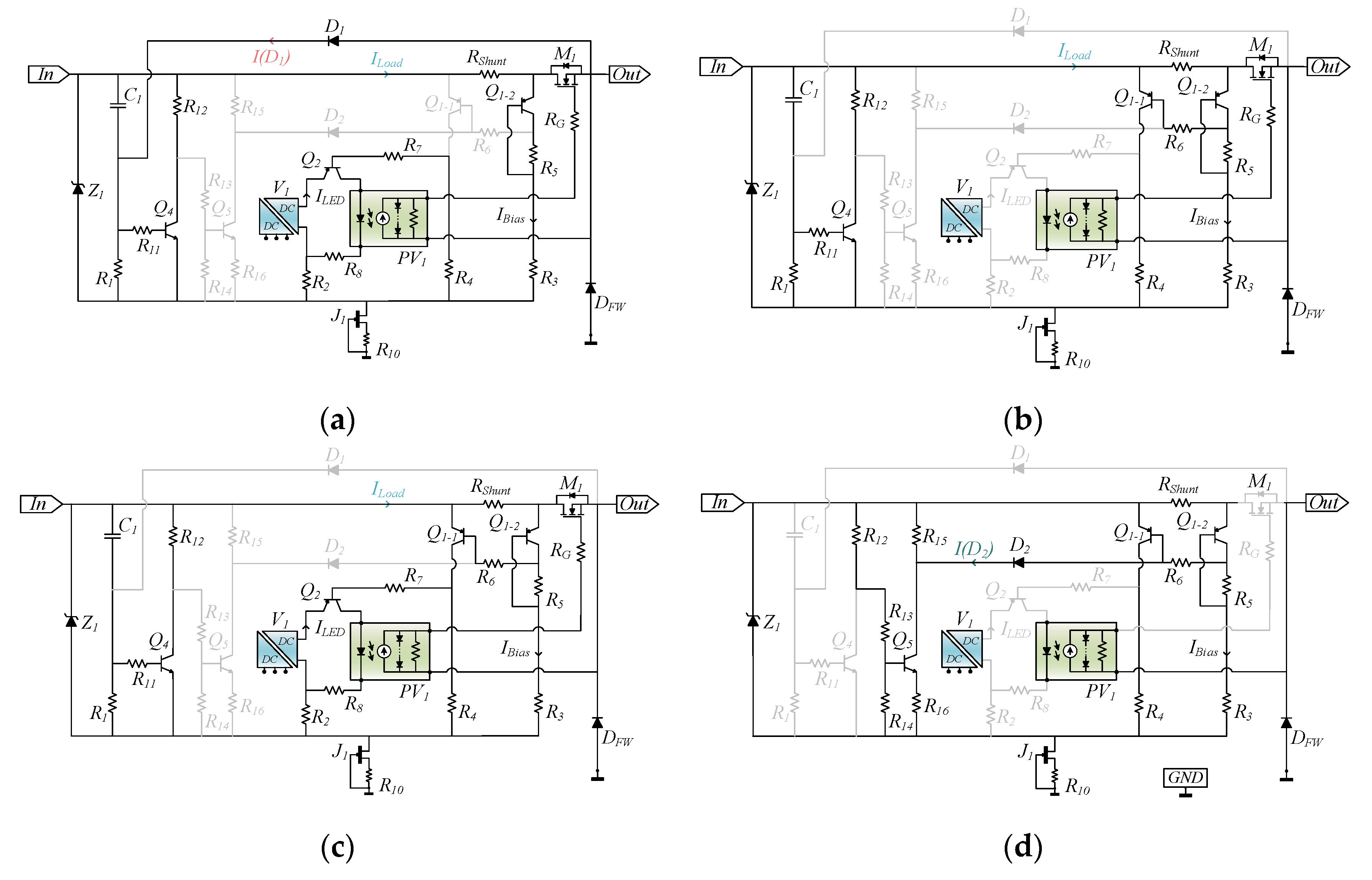
3.1. STO with Current Limitation
3.2. FTO with Current Limitation
3.3. FTO without Current Limitation (Circuit Breaker)
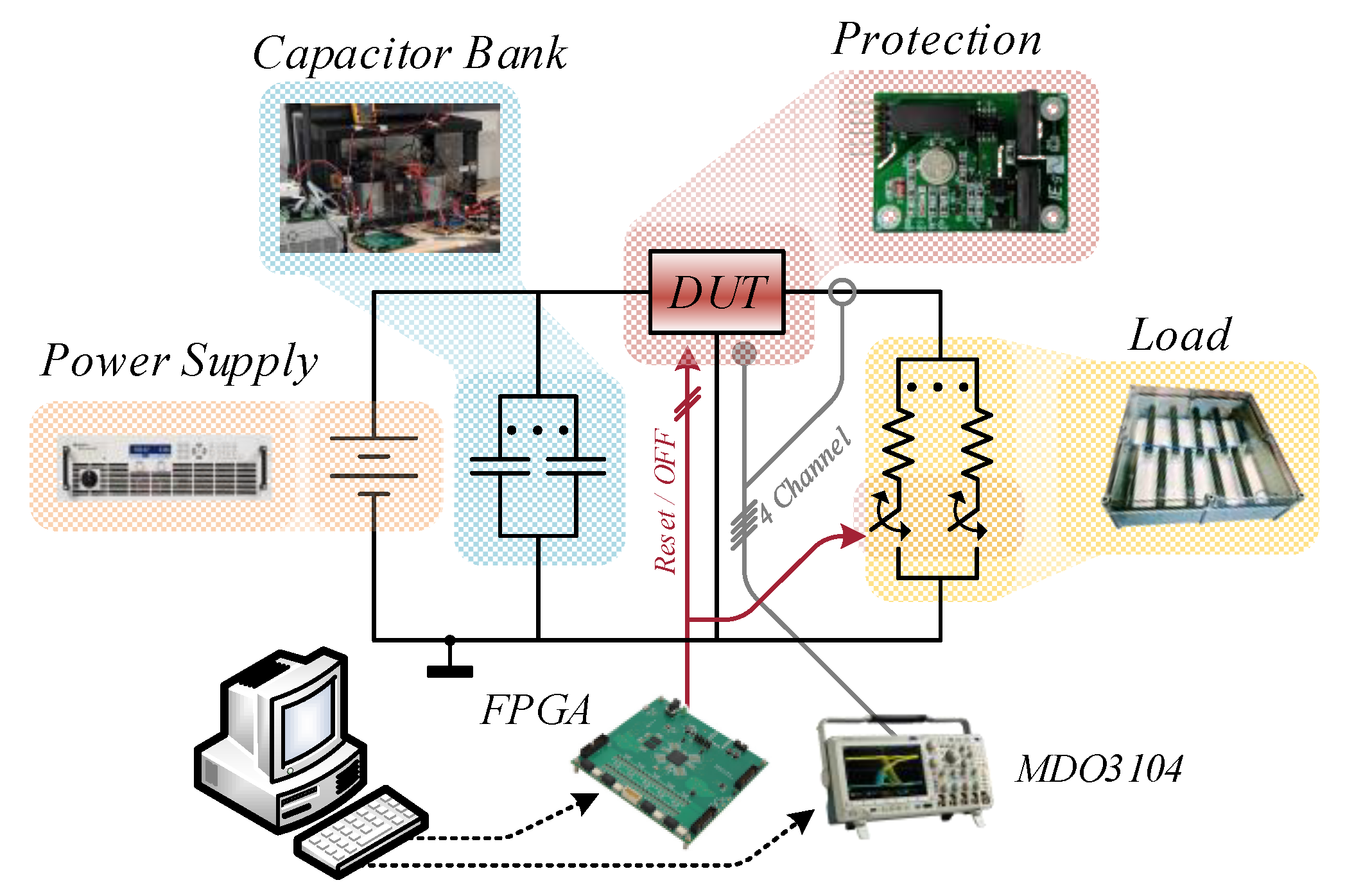
4. Materials and Methods
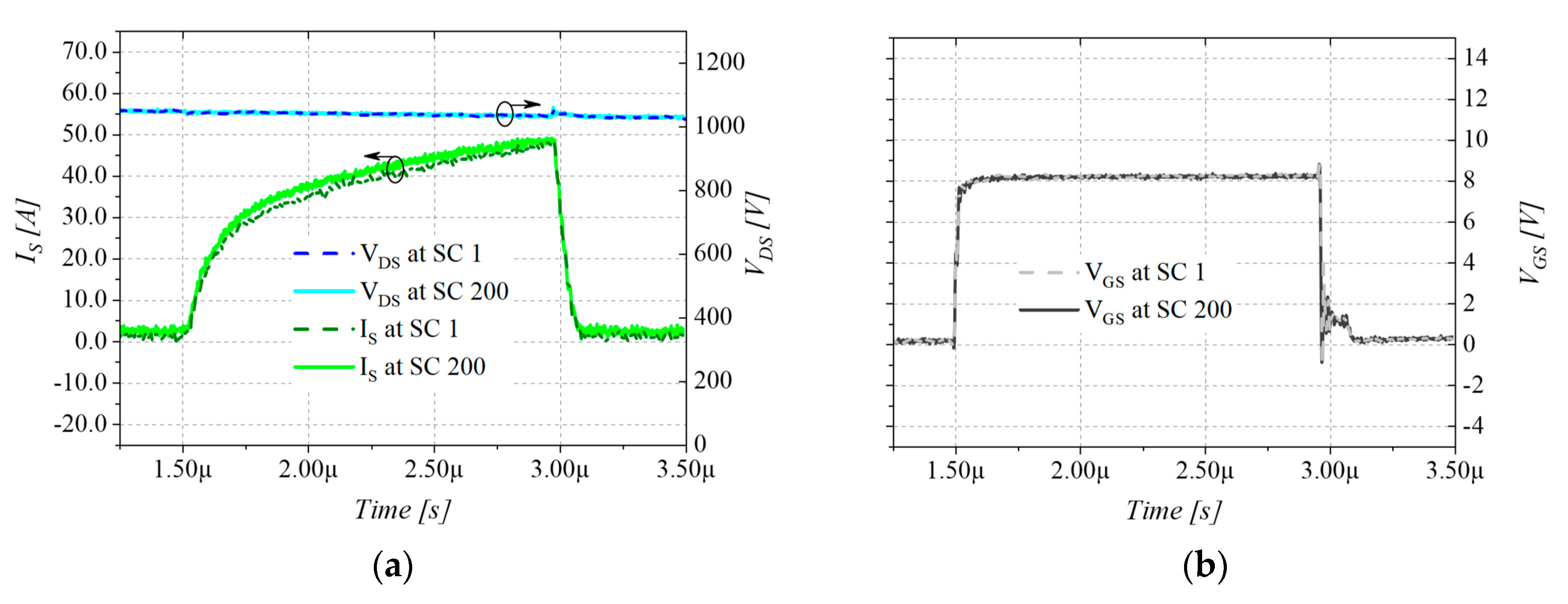
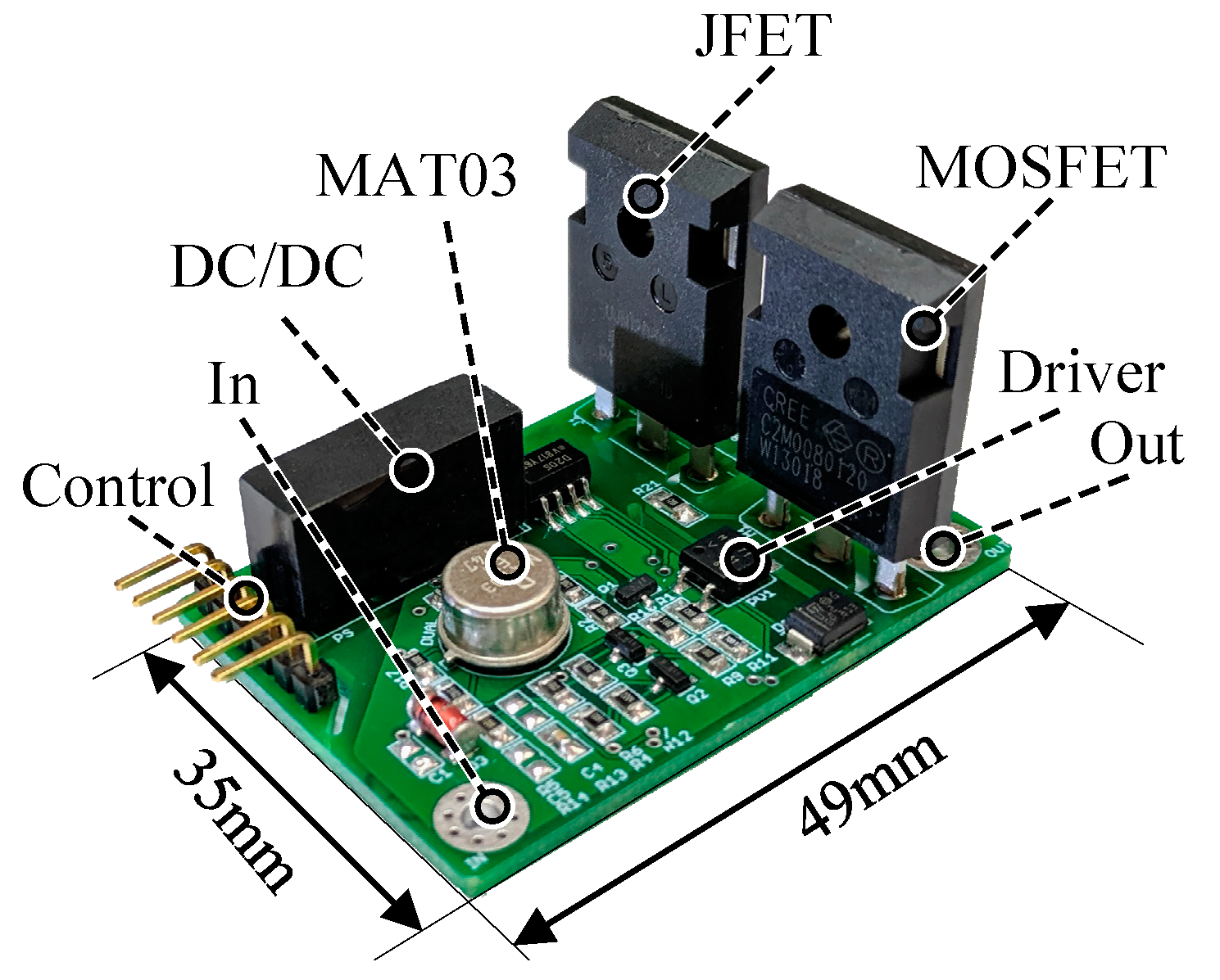
4.1. Setup and Main Transistor Robustness
4.2. SSCB-LCL Design and Test Plan
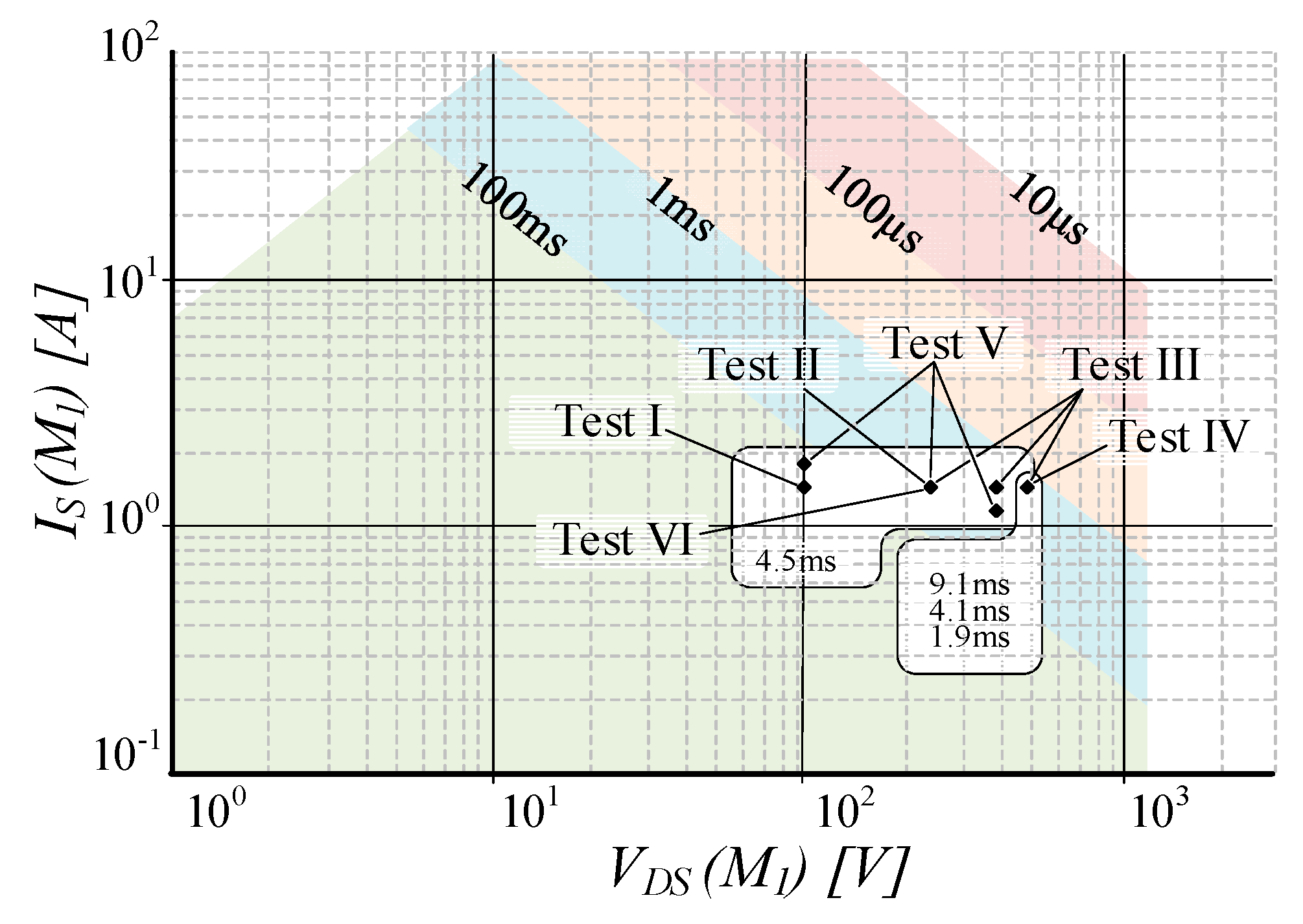
5. Experimental Results and Discussion
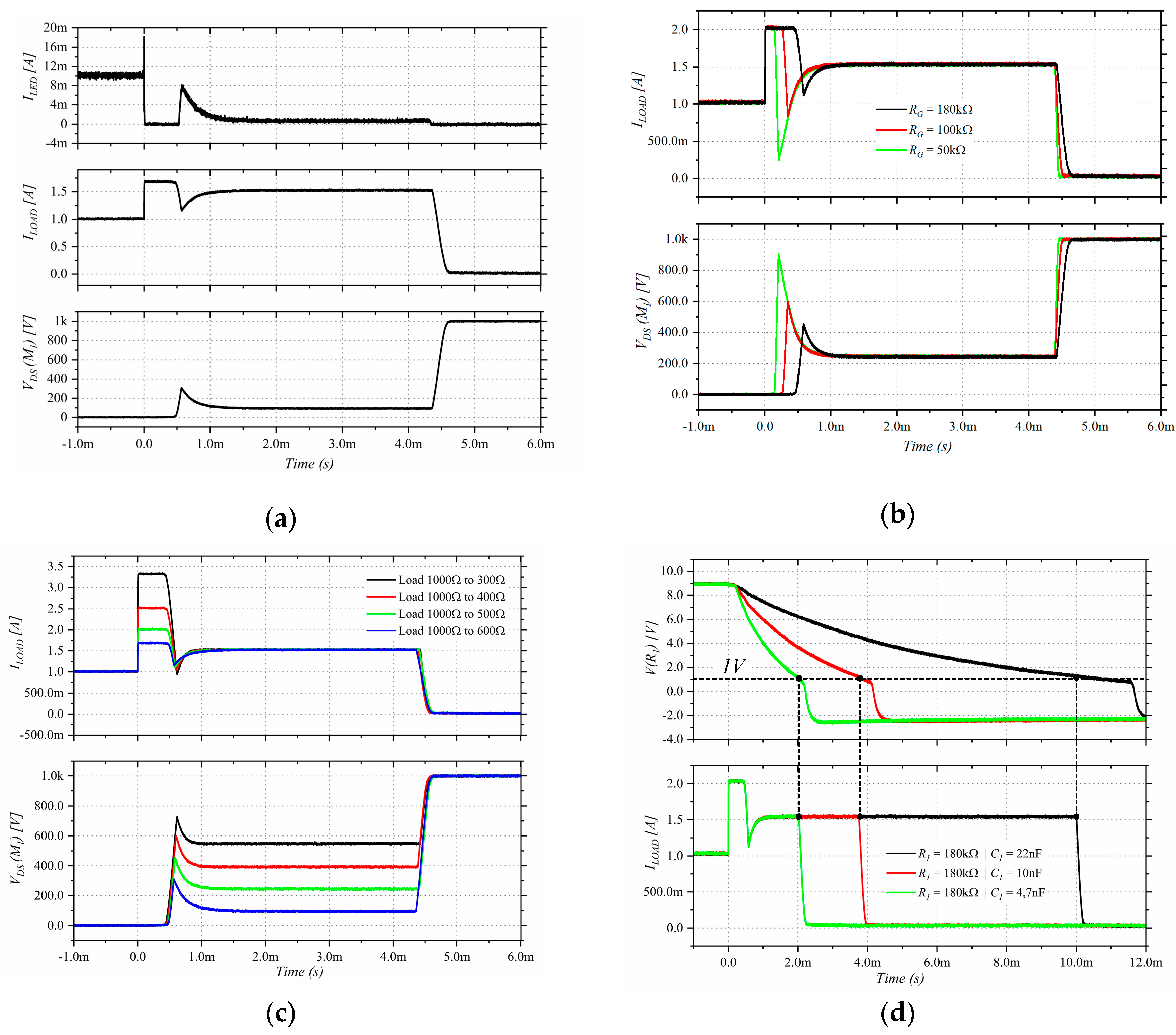
5.1. Basic Operation
5.2. RG Sweep
5.3. Overload Sweep
5.4. Sweep
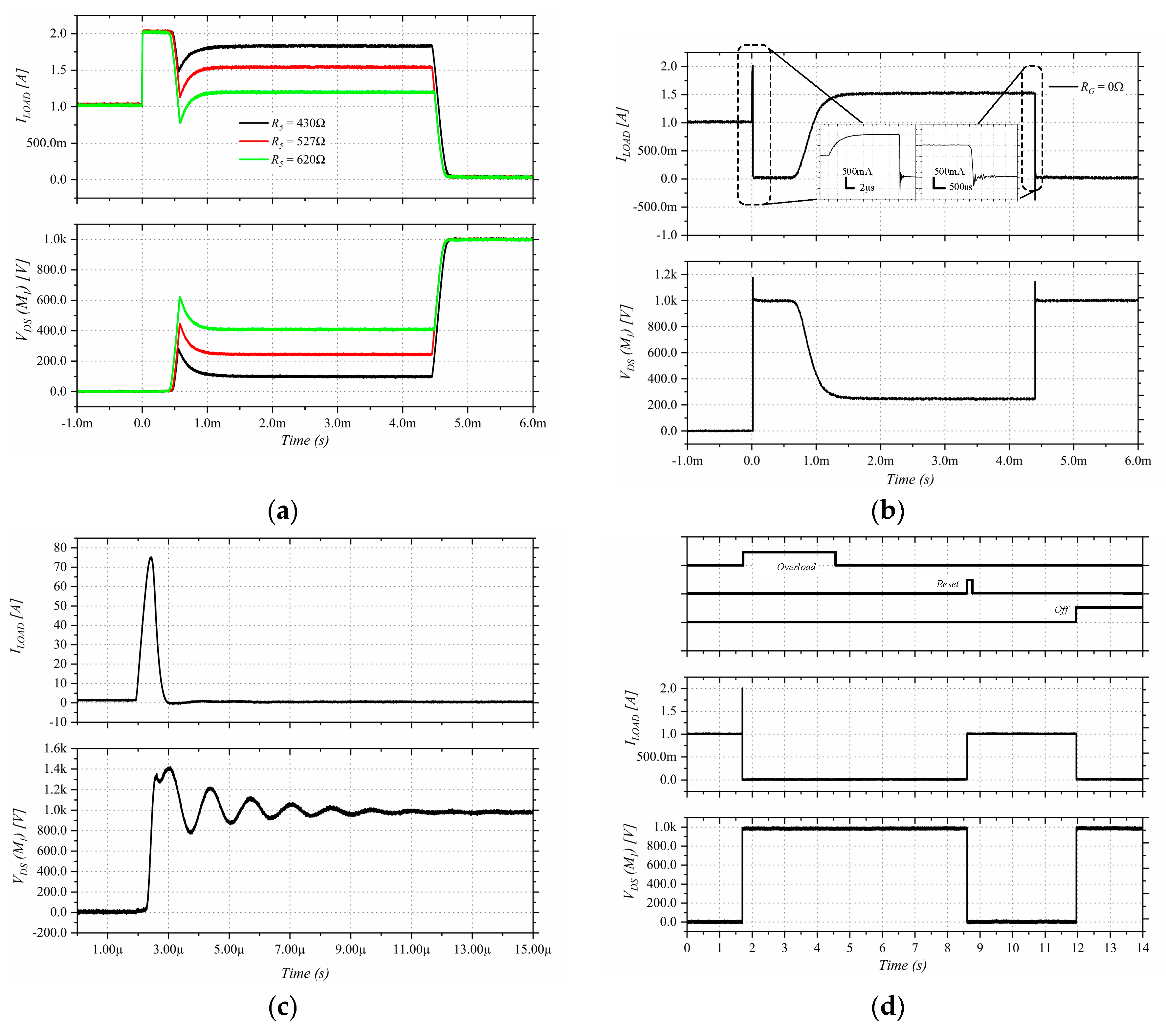
5.5. Sweep
5.6. FTO with Current Limitation
5.7. Short-Circuit
5.8. Tele Command Test
6. Conclusions
Author Contributions
Funding
Acknowledgments
Conflicts of Interest
Abbreviations
| CISS | M1 input capacitance. |
| CRSS | M1 reverse transfer capacitance. |
| gfs | M1 transconductance. |
| ILoad | Load current. |
| ILimit | Programmed current limit. |
| Fault current. | |
| IBias | Bias current of current limiting circuit. |
| ILED | PV1 light emitting diode current. |
| Maximum PV1 light emitting diode current. | |
| ISC | PV1 photocell short-circuit current. |
| IR | PV1 photocell diode saturation current. |
| M1 | Main power transistor. |
| PV1 | Photovoltaic driver. |
| M1 gate charge at its threshold voltage. | |
| M1 gate charge at the open circuit voltage of the PV1 photocell. | |
| RShunt | Shunt resistor. |
| RG | M1 gate resistor. |
| Equivalent resistance of PV1 turn-off circuit during off state. | |
| Equivalent resistance of PV1 turn-off circuit during on state. | |
| tLatching | Latching time. |
| Turn-on delay. | |
| Turn-off delay. | |
| Turn-off delay in STO configuration. | |
| Turn-off delay in FTO configuration. | |
| Current limitation response time. | |
| tlmt | Limitation time. |
| tturn-On | Turn-on time. |
| tturn-Off | Turn-off time. |
| trv | Voltage rise time. |
| tfi | Current fall time. |
| VGS | M1 gate-source voltage. |
| Vgp | M1 gate-source plateau voltage. |
| V(Z1) | Reference voltage. |
| VLED | PV1 light emitting diode forward voltage |
| V1 | Auxiliary power supply. |
| VOC | PV1 photocell open circuit voltage. |
| Vth | M1 threshold voltage. |
| Vin | SSCB-LCL input voltage. |
| α | PV1 light emitting diode current to photocell current. |
| β | Bipolar junction transistor current gain. |
| k | Boltzmann’s constant. |
| q | Electron charge. |
| FTO | Fast Turn Off. |
| STO | Slow Turn Off. |
References
- Hatziargyriou, N.D. Microgrids: An Overview of Ongoing Research, Development, and Demonstration Projects Environmental Energy Technologies Division. IEEE Power Energy Mag. 2007, 5, 78–94. [Google Scholar] [CrossRef]
- Kakigano, H.; Miura, Y.; Ise, T. Low-voltage bipolar-type dc microgrid for super high quality distribution. IEEE Trans. Power Electron. 2010, 25, 3066–3075. [Google Scholar] [CrossRef]
- Elvira, D.G.; Blaví, H.V.; Pastor, À.C.; Salamero, L.M. Efficiency optimization of a variable bus voltage DC microgrid. Energies 2018, 11, 3090. [Google Scholar] [CrossRef]
- Madduri, P.A.; Poon, J.; Rosa, J.; Podolsky, M.; Brewer, E.A.; Sanders, S.R. Scalable DC Microgrids for Rural Electrification in Emerging Regions. IEEE J. Emerg. Sel. Top. Power Electron. 2016, 4, 1195–1205. [Google Scholar] [CrossRef]
- Rodriguez-Diaz, E.; Chen, F.; Vasquez, J.C.; Guerrero, J.M.; Burgos, R.; Boroyevich, D. Voltage-Level Selection of Future Two-Level LVdc Distribution Grids: A Compromise between Grid Compatibiliy, Safety, and Efficiency. IEEE Electrif. Mag. 2016, 4, 20–28. [Google Scholar] [CrossRef]
- Ryu, M.-H.; Kim, H.-S.; Baek, J.-W.; Kim, H.-G.; Jung, J.-H. Effective Test Bed of 380-V DC Distribution System Using Isolated Power Converters. IEEE Trans. Ind. Electron. 2015, 62, 4525–4536. [Google Scholar] [CrossRef]
- Salomonsson, D.; Söder, L.; Sannino, A. Protection of low-voltage DC microgrids. IEEE Trans. Power Deliv. 2009, 24, 1045–1053. [Google Scholar] [CrossRef]
- Chae, S.; Park, J.; Oh, S. Series DC Arc Fault Detection Algorithm for DC Microgrids Using Relative Magnitude Comparison. IEEE J. Emerg. Sel. Top. Power Electron. 2016, 4, 1270–1278. [Google Scholar] [CrossRef]
- Zhang, L.; Tai, N.; Huang, W.; Liu, J.; Wang, Y. A review on protection of DC microgrids. J. Mod. Power Syst. Clean Energy 2018, 6, 1113–1127. [Google Scholar] [CrossRef]
- Bui, D.M.; Chen, S.-L.; Lien, K.-Y.; Jiang, J.-L. Fault protection solutions appropriately used for ungrounded low-voltage AC microgrids. In Proceedings of the 2015 IEEE Innovative Smart Grid Technologies-Asia (ISGT ASIA), Bangkok, Thailand, 3–6 November 2015; pp. 1–6. [Google Scholar]
- Shukla, A.; Demetriades, G.D. A Survey on Hybrid Circuit-Breaker Topologies. IEEE Trans. Power Deliv. 2015, 30, 627–641. [Google Scholar] [CrossRef]
- Javed, W.; Chen, D.; Farrag, M.E.; Xu, Y. System configuration, fault detection, location, isolation and restoration: A review on LVDC microgrid protections. Energies 2019, 12, 1001. [Google Scholar] [CrossRef]
- Izquierdo, D.; Barrado, A.; Raga, C.; Sanz, M.; Lázaro, A. Protection devices for aircraft electrical power distribution systems: State of the art. IEEE Trans. Aerosp. Electron. Syst. 2011, 47, 1538–1550. [Google Scholar] [CrossRef]
- Chen, Z.; Yu, Z.; Zhang, X.; Wei, T.; Lyu, G.; Qu, L.; Huang, Y.; Zeng, R. Analysis and Experiments for IGBT, IEGT, and IGCT in Hybrid DC Circuit Breaker. IEEE Trans. Ind. Electron. 2018, 65, 2883–2892. [Google Scholar] [CrossRef]
- Shen, Z.J.; Sabui, G.; Miao, Z.; Shuai, Z. Wide-bandgap solid-state circuit breakers for DC power systems: Device and circuit considerations. IEEE Trans. Electron Devices 2015, 62, 294–300. [Google Scholar] [CrossRef]
- Miao, Z.; Sabui, G.; Roshandeh, A.M.; Shen, Z.J. Design and Analysis of DC Solid-State Circuit Breakers Using SiC JFETs. IEEE J. Emerg. Sel. Top. Power Electron. 2016, 4, 863–873. [Google Scholar] [CrossRef]
- Sato, Y.; Tanaka, Y.; Fukui, A.; Yamasaki, M.; Ohashi, H. SiC-SIT circuit breakers with controllable interruption voltage for 400-V DC distribution systems. IEEE Trans. Power Electron. 2014, 29, 2597–2605. [Google Scholar] [CrossRef]
- Ren, Y.; Yang, X.; Zhang, F.; Wang, K.; Chen, W.; Wang, L.; Pei, Y. A Compact Gate Control and Voltage-Balancing Circuit for Series-Connected SiC MOSFETs and Its Application in a DC Breaker. IEEE Trans. Ind. Electron. 2017, 64, 8299–8309. [Google Scholar] [CrossRef]
- Mazumder, S.K. An Overview of Photonic Power Electronic Devices. IEEE Trans. Power Electron. 2016, 31, 6562–6574. [Google Scholar] [CrossRef]
- Veliadis, V.; Steiner, B.; Lawson, K.; Bayne, S.B.; Urciuoli, D.; Ha, H.C. Suitability of N-ON Recessed Implanted Gate Vertical-Channel SiC JFETs for Optically Triggered 1200 v Solid-State Circuit Breakers. IEEE J. Emerg. Sel. Top. Power Electron. 2016, 4, 874–879. [Google Scholar] [CrossRef]
- Wilkins, M.M.; Ishigaki, M.; Provost, P.O.; Masson, D.; Fafard, S.; Valdivia, C.E.; Dede, E.M.; Hinzer, K. Ripple-free boost-mode power supply using photonic power conversion. IEEE Trans. Power Electron. 2019, 34, 1054–1064. [Google Scholar] [CrossRef]
- Marroquí, D.; Garrigós, A.; Blanes, J.M.; Gutiérrez, R.; Maset, E.; Ramírez, D. SIC based solid state protections switches for space applications. In Proceedings of the 2017 19th European Conference Power Electronics Applications EPE 2017 ECCE Europe, Warsaw, Poland, 11–14 September 2017; pp. 1–8. [Google Scholar]
- Li, H.; Yu, R.; Zhong, Y.; Yao, R.; Liao, X.; Chen, X. Design of 400 V Miniature DC Solid State Circuit Breaker with SiC MOSFET. Micromachines 2019, 10, 314. [Google Scholar] [CrossRef] [PubMed]
- Wang, J.; Jiang, X.; Li, Z.; Shen, Z.J. Short-Circuit Ruggedness and Failure Mechanisms of Si/SiC Hybrid Switch. IEEE Trans. Power Electron. 2019, 34, 2771–2780. [Google Scholar] [CrossRef]
- Qin, H.; Mo, Y.; Xun, Q.; Zhang, Y.; Dong, Y. A Digital-Controlled SiC-Based Solid State Circuit Breaker with Soft Switch-Off Method for DC Power System. Electronics 2019, 8, 837. [Google Scholar] [CrossRef]
- Marroqui, D.; Garrigos, A.; Blanes, J.M.; Gutierrez, R.; Maset, E.; Iannuzzo, F. SiC MOSFET vs SiC/Si Cascode short circuit robustness benchmark. Microelectron. Reliab. 2019, 100, 113429. [Google Scholar] [CrossRef]


| Description | Constant Parameters | Variable Parameter | ||
|---|---|---|---|---|
| STO with Current Limiter | Test I Basic Operation | SL = 1 to 1.66 A = 1.5 A | Load = 1000 to 600 Ω R1 = 180 kΩ, C1 =10 nF R5 = 527 Ω, RShunt = 50 mΩ RG = 180 kΩ | |
Sweep | = 1.5 A | Load = 1000 to 500 Ω R1 = 180 k, C1 = 10 nF R5 = 527 Ω, RShunt = 50 mΩ | = [50, 100, 180] kΩ | |
| Test III Overload Sweep | = 1.5 A | R1 = 180 kΩ, C1 = 10 nF R5 = 527Ω, RShunt = 50 mΩ RG = 180 kΩ | LS = 1 A to [1.6, 2, 2.5, 3.3] A Load = 1000 Ω to [600, 500, 400, 300] Ω | |
Sweep | = 1.5 A | Load = 1000 to 500 Ω R5 = 527 Ω, RShunt = 50 mΩ R1 = 180 kΩ, RG = 180 kΩ | = [1.9, 4.1, 9.1] ms C1 = [4.7, 10, 22] nF | |
Sweep | = 4.5 ms | Load = 1000 to 500 Ω R1 = 180 k, C1 = 10 nF RG = 180 kΩ, RShunt = 50 mΩ | = [1.25, 1.53, 1.80] A R5 = [430, 527, 620] Ω | |
| Test VI FTO with Current Limitation | = 1.5 A | Load = 1000 to 500 Ω R1 = 180 k, C1 = 10 nF R5 = 527 Ω, RShunt = 50 mΩ RG = 0 Ω | ||
| Circuit Breaker | Test VII Short-circuit | = 1.5 A | Load = 1000 Ω to SC R5 = 527 Ω, RShunt = 50 mΩ R1 = 510 Ω, C1 = 1 nF RG = 0 Ω | |
| Test VIII Tele Command | = 1.5 A | Load = 1000 to 500 Ω R5 = 527 Ω, RShunt = 50 mΩ R1 = 510 Ω, C1 = 1 nF RG = 0 Ω | ||
| Description | Parameter | Variable | Theoretical | Measured | ||
|---|---|---|---|---|---|---|
| STO with Current Limiter | Test II Sweep | RG | 50 kΩ | 127 µs | 146 µs | |
| 100 kΩ | 242 µs | 264 µs | ||||
| 180 kΩ | 427 µs | 462 µs | ||||
| ALL | 1.3 ms | 900 µs | ||||
| Test IV Sweep | C1 | 4.7 nF | 1.9 ms | 2.2 ms | ||
| 10 nF | 4.1 ms | 4.0 ms | ||||
| 22 nF | 9.1 ms | 10.2 ms | ||||
| Test V Sweep | R5 | 430 Ω | 1.25 A | 1.19 A | ||
| 527 Ω | 1.53 A | 1.54 A | ||||
| 620 Ω | 1.80 A | 1.83 A | ||||
| Test VI Fast Turn-Off with Current Limitation | N/A | N/A | 16 µs | |||
| N/A | 570 µs | 700 µs | ||||
| N/A | 770 µs | 700 µs | ||||
© 2019 by the authors. Licensee MDPI, Basel, Switzerland. This article is an open access article distributed under the terms and conditions of the Creative Commons Attribution (CC BY) license (http://creativecommons.org/licenses/by/4.0/).
Share and Cite
Marroqui, D.; Garrigos, A.; Blanes, J.M.; Gutierrez, R. Photovoltaic-Driven SiC MOSFET Circuit Breaker with Latching and Current Limiting Capability. Energies 2019, 12, 4585. https://doi.org/10.3390/en12234585
Marroqui D, Garrigos A, Blanes JM, Gutierrez R. Photovoltaic-Driven SiC MOSFET Circuit Breaker with Latching and Current Limiting Capability. Energies. 2019; 12(23):4585. https://doi.org/10.3390/en12234585
Chicago/Turabian StyleMarroqui, David, Ausias Garrigos, Jose M. Blanes, and Roberto Gutierrez. 2019. "Photovoltaic-Driven SiC MOSFET Circuit Breaker with Latching and Current Limiting Capability" Energies 12, no. 23: 4585. https://doi.org/10.3390/en12234585