Article

Investigations on EMI Mitigation Techniques: Intent to Reduce Grid-Tied PV Inverter Common Mode Current and Voltage

by
Umashankar Subramaniam
1,*,
Sagar Mahajan Bhaskar
1,
Dhafer J.Almakhles
1,
Sanjeevikumar Padmanaban
2 and
Zbigniew Leonowicz
3
1
Renewable Energy Lab, Department of Communications and Networks, College of Engineering, Prince Sultan University (PSU), Riyadh 66833, Saudi Arabia
2
Department of Energy Technology, Aalborg University, 6700 Esbjerg, Denmark
3
Faculty of Electrical Engineering, Wroclaw University of Science and Technology, Wyb. Wyspianskiego 27, 50370 Wroclaw, Poland
*
Author to whom correspondence should be addressed.
Energies 2019, 12(17), 3395; https://doi.org/10.3390/en12173395
Submission received: 1 August 2019 / Revised: 25 August 2019 / Accepted: 29 August 2019 / Published: 3 September 2019

Abstract

:
Power inverters produce common mode voltage (CMV) and common mode current (CMC) which cause high-frequency electromagnetic interference (EMI) noise, leakage currents in electrical drives application and grid-connected systems, which consequently drops the efficiency of the system considerably. This CMV can be mitigated by designing suitable EMI filters and/or investigating the effects of different modulation strategies. In this paper, the effect of various modulation techniques over CMV and CMC are investigated for two-level and three-level inverters. It is observed that the modified third harmonic injection method reduced the CMV and CMC in the system by 60%. This modified pulse width modulation (PWM) technique is employed along with EMI chokes which results in reduced distortion of the system.

1. Introduction

The PV-grid connected power inverter is a necessary part of the PV to electrical energy conversion system [1]. The quality of the voltage depends upon three phenomenons of voltage harmonics, voltage dips or swells and flicker [2]. In the present day, the intense use of electrical loads driven by power electronics (e.g., personal computers) has led to a severe increase of current harmonics drawn from the distribution system. These current harmonics, due to the impedance of the network, induce voltage harmonics into the utility. Voltage dips originate from fault currents in the electrical system or inrush currents of electrical motors and transformers [
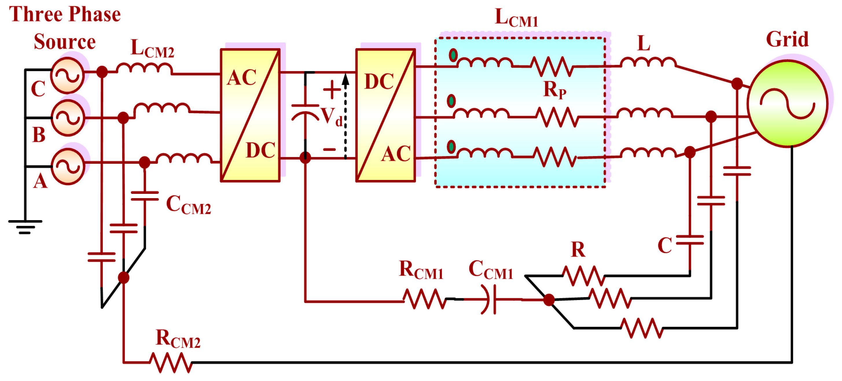
3]. The common mode circuit is formed in between Photo Voltaiacs (PVs) and the grid, as well as ground due to parasitic capacitance and deficiencies in galvanic isolation between the grid and PVs [1,4]. Electromagnetic interference (EMI) is the main source of unexpected transition at the output port of variable frequency drive (VFD). The fall time and rise time of semiconductor devices (employed in the converter section of VFD) are used to determine voltage transition times. These voltage transition times are around 100ns which is very fast. As a result, high dv/dt occurs. In the stray line to ground cables and capacitor, the magnitude of common mode noise current is higher if dv/dt is higher [4]. These noise currents affect the control signals and are the main source of EMI.
The instability and disturbances occur at the supply side due to the utilization of a higher number of power devices and components for energy conversion [5]. Mainly, non-linear devices are responsible for this instability and disturbances. Due to this, harmonics are introduced in the power system. These harmonics causes EMI-related problems, overheating in the equipment, and damage the devices, etc. Inverter common mode voltage (CMV) and its leakage current are the primary concerns of radiated EMI. Noise with high-frequency components is emitted in the form of electromagnetic energy and may interfere with other components and equipment at the common coupling point [6]. To minimize common currents, commonly used methods are [1] improved power inverter structures with common mode current (CMC) suppression capabilities and advanced pulse width modulation (PWM) schemes [7], and (2) the addition of EMI filters [8] and bridge inverter topology based on DC and AC bypass [9]. It is also notable that the circuitry with fast switching semiconductors produces a very high amount di/dt and dv/dt and which is one of the reasons for the cause of EMI [10]. Decoupling effect-based configurations with constant CMV [11] and transformerless power converter configurations [12] are proposed to suppress CMC. The CM loop impedance can be increased in order to suppress current in CM loop effectively. In [13], the mid-point of DC and AC side voltage nodes are connected to the proposed new CM internal loop scheme in order to suppress CMC. In [14], a novel modulation scheme is presented to control inverter power switches in order to reduce CMC. In [15], a CM internal loop is formed by employing the RC branch in between the negative bus of DC and output terminals. However, detailed analysis of the CMC and its effect on CMC high-frequency components are not presented. In [16], a new scheme based on a dual CM internal loop for a PV grid-connected transformer-less system is proposed to suppress CMC high-frequency components. In [17] characteristics and analysis of the CMV based on the simplified modelling of a cascaded H-bridge power transformer and PWM strategy are presented under the fault grid condition and balanced condition. In [18], in order to reduce CM leakage current, a new hybrid modulation strategy is suggested. The suggested method is efficient and has reactive power provision with low distortion in the current. Filters at the input/output terminal are employed to suppress this unwanted emission or electromagnetic interference (EMI) [19,20]. Generally, filters are employed at the connector of power supply in order to restrict disturbance signals [21,22]. Generally, classical filters are designed by utilizing passive components, i.e., inductor and capacitor values to attenuate high-frequency voltage and current components [23,24]. However, the performance of the filter is dependent on the value of L and C and has limited achievable insertion loss that should be improved to meet the necessary condition. Moreover, passive filters are bulky, costly, and their volume mainly depends on the inductor size which is approximately directly proportional to the required attenuation. Moreover, there is always uncertainty in parasitic components. In order to reduce CMV and current effect, active [25] and passive filters [
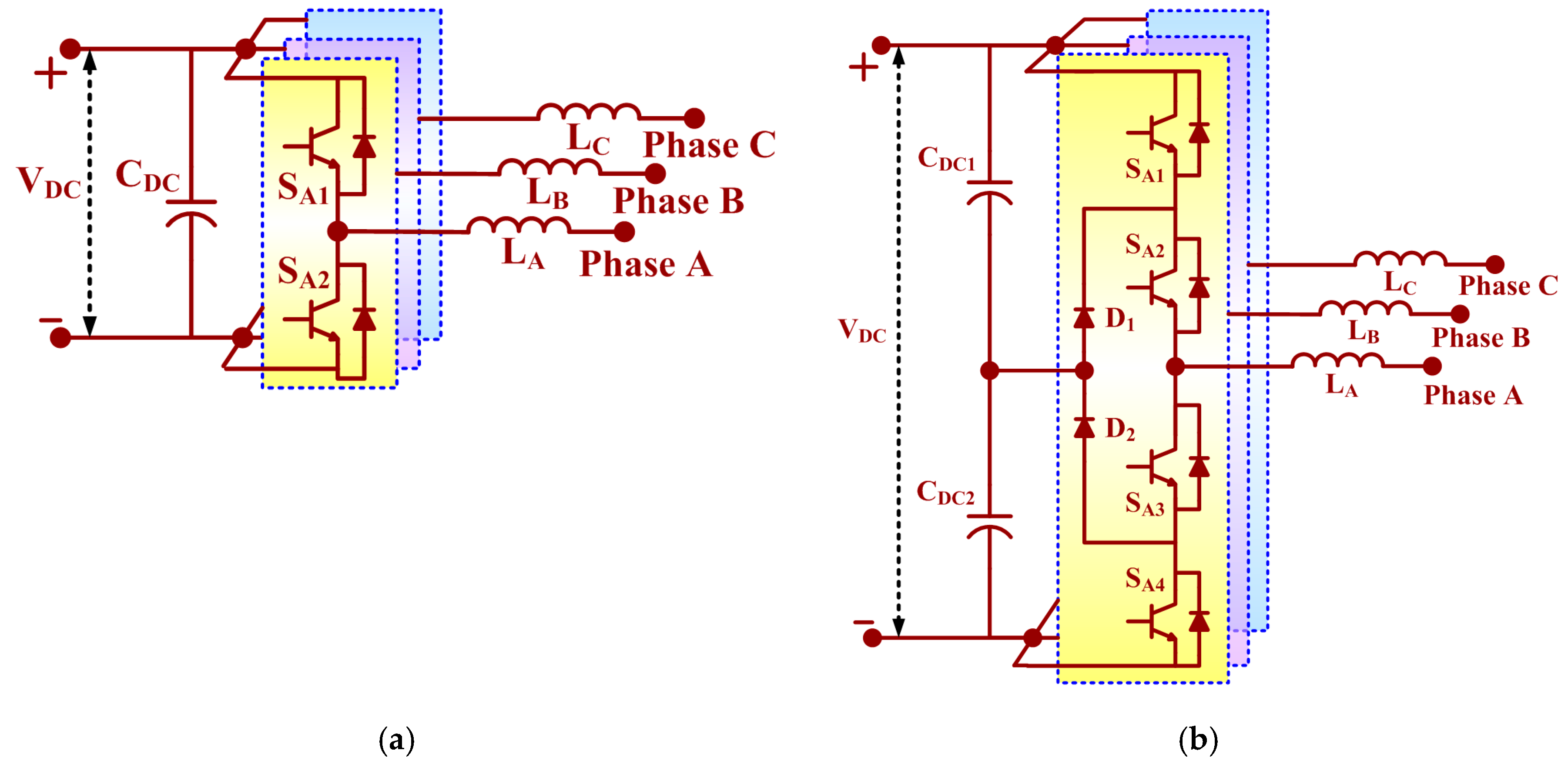
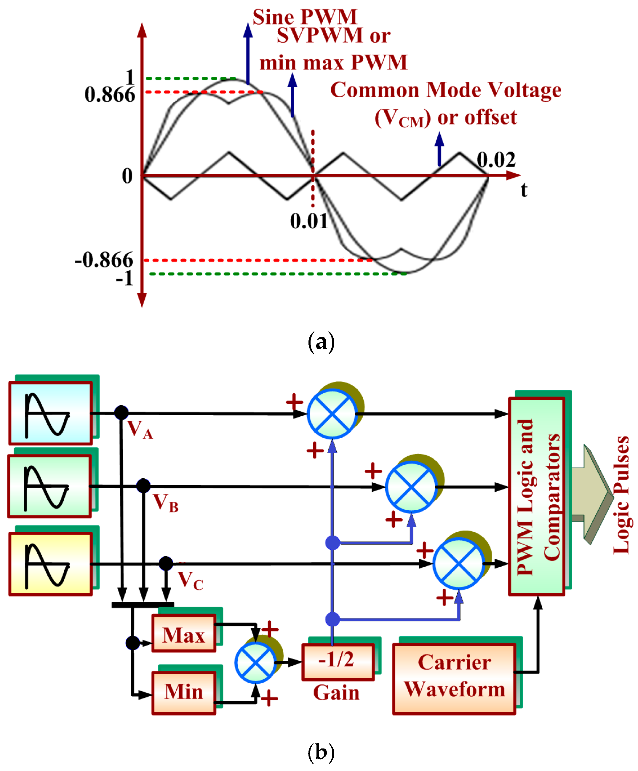
26] are suggested. However, these filters increase the size, cost of the system, and control of the equipment. As a result, it is good to advance control strategies in order to reduce the CMV’s effect. In order to eliminate or reduce CMV, numerous control schemes are proposed based on the modulation strategy, such as the Sine PWM for three-level neutral point clamped (NPC) inverter [27], PWM based on non-nearest vectors, Space Vector PWM for high-level inverters [28,29], etc. In [30], a detailed comparison of SPWM and SVPWM techniques are presented for the three-phase inverter. Nevertheless, similar PWM schemes presented in [31,32] are restricted to 3–5 levels inverters. Synchronous reference frame and feedforward reference frame-based dynamic voltage restorer comparative study are presented in [33]. In [34], a new SVPWM scheme is presented with advanced features, such as the proposed scheme, which is suitable for inverters with any number of levels, zero CMVs can be achieved at any modulation index, the simple realization of CMV vectors, fast control scheme, etc. In [35], a new methodology called the spread spectrum (SS) technique is presented in order to reduce EMI of power converters over a wide range of frequency. However, this SS technique is competent to reduce EMI levels around 5–10 dB [36]. Based on the output voltage waveform and its alignment, another technique is suggested in [37,38]. However, this methodology has a specific application. In [39], a new technique based on software is presented to reduce EMI. The methodology is suitable for single- and three-phase power inverters. In [40], analysis on the CM EMI and methodology to mitigate EMI in power inverters is discussed by using a delay compensation technique. In order to mitigate EMI, numerous passive filter methods are proposed based on the phases of the noise signal. In [41], a common mode-coupled inductor is designed in order to mitigate common mode noise. Nevertheless, differential mode noise is not able to be reduced by using this technique. Hence, later, a new method based on an integrated choke is presented in order to reduce differential, as well as common mode, noise at the same time [42].
In [43], a new method based on the parasitic component’s determination is presented in order to predict EMI noise. In [44,45], computer-based three-dimensional modelling is presented for the noise current prediction by determining the value of parasitic components. A novel EMI filter is discussed with sufficient attenuation with a limited LC value in order to CM EMI [46]. Nevertheless, filters are additional components and increase the volume and cost of the system. Moreover, the implementation of the effective filter is important and the effort for the mitigation of EMI without knowing the system may degrade the performance and require additional cost. To reduce CM voltage, a new impedance balancing method is presented instead of impedance mismatching [47]. The three-phase phase-lock-loop for a distorted utility is discussed in [48]. In [49], controllable devices are used and active filters are presented to suppress CMC generated by the CMV method, called the active noise cancellation scheme, in order to mitigate the noise signal [50]. In [51], a new wavelet transform-based technique to mitigate EMI noise in power converter is presented with a frequency band of 3–30 MHz.
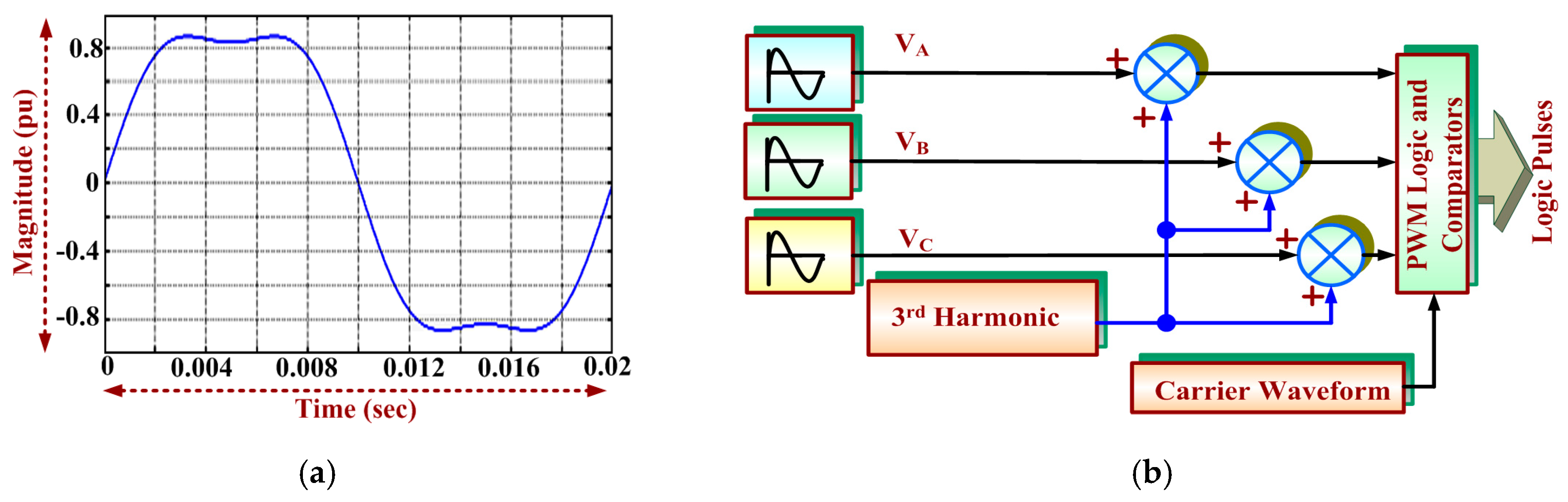
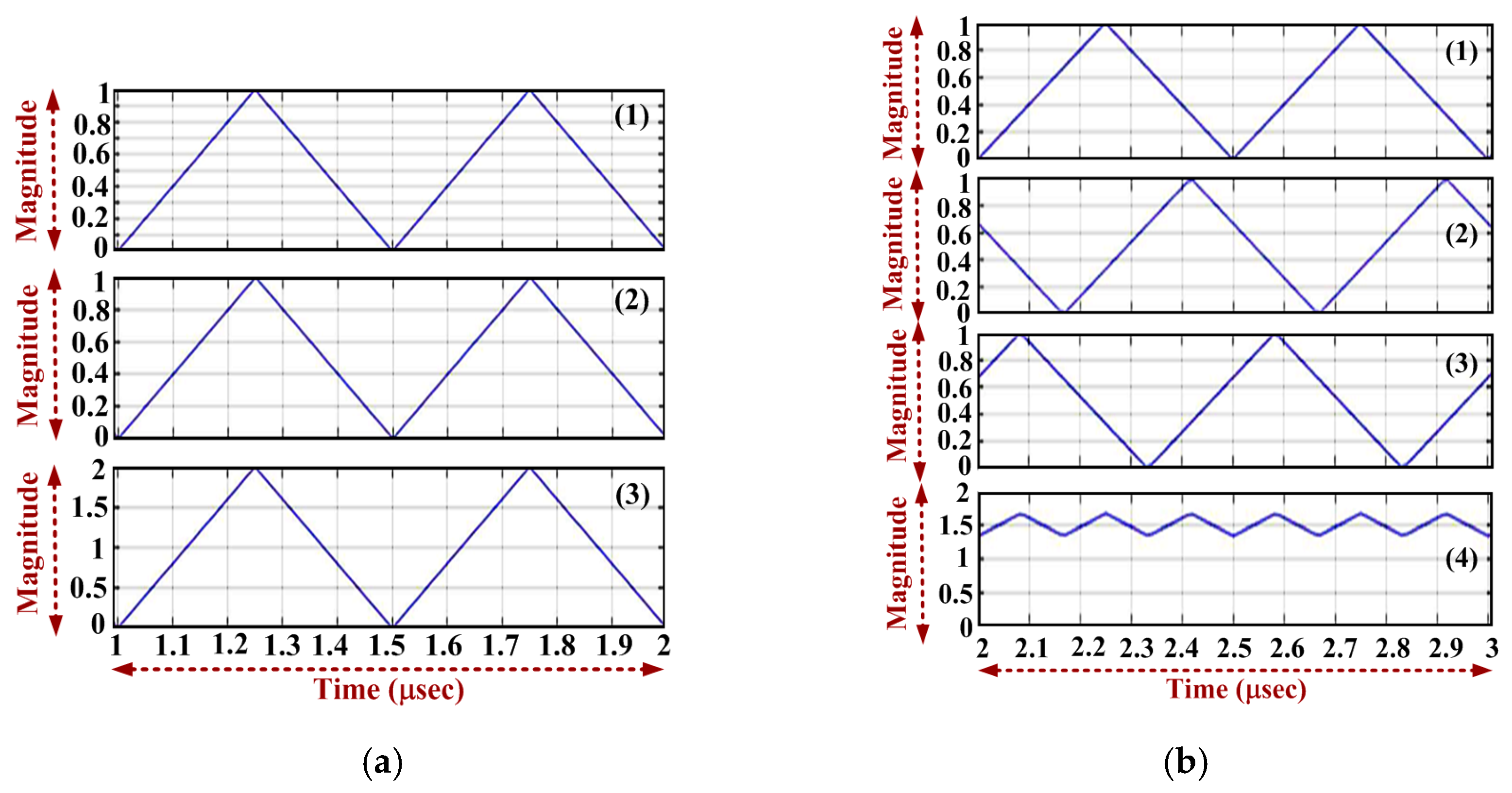
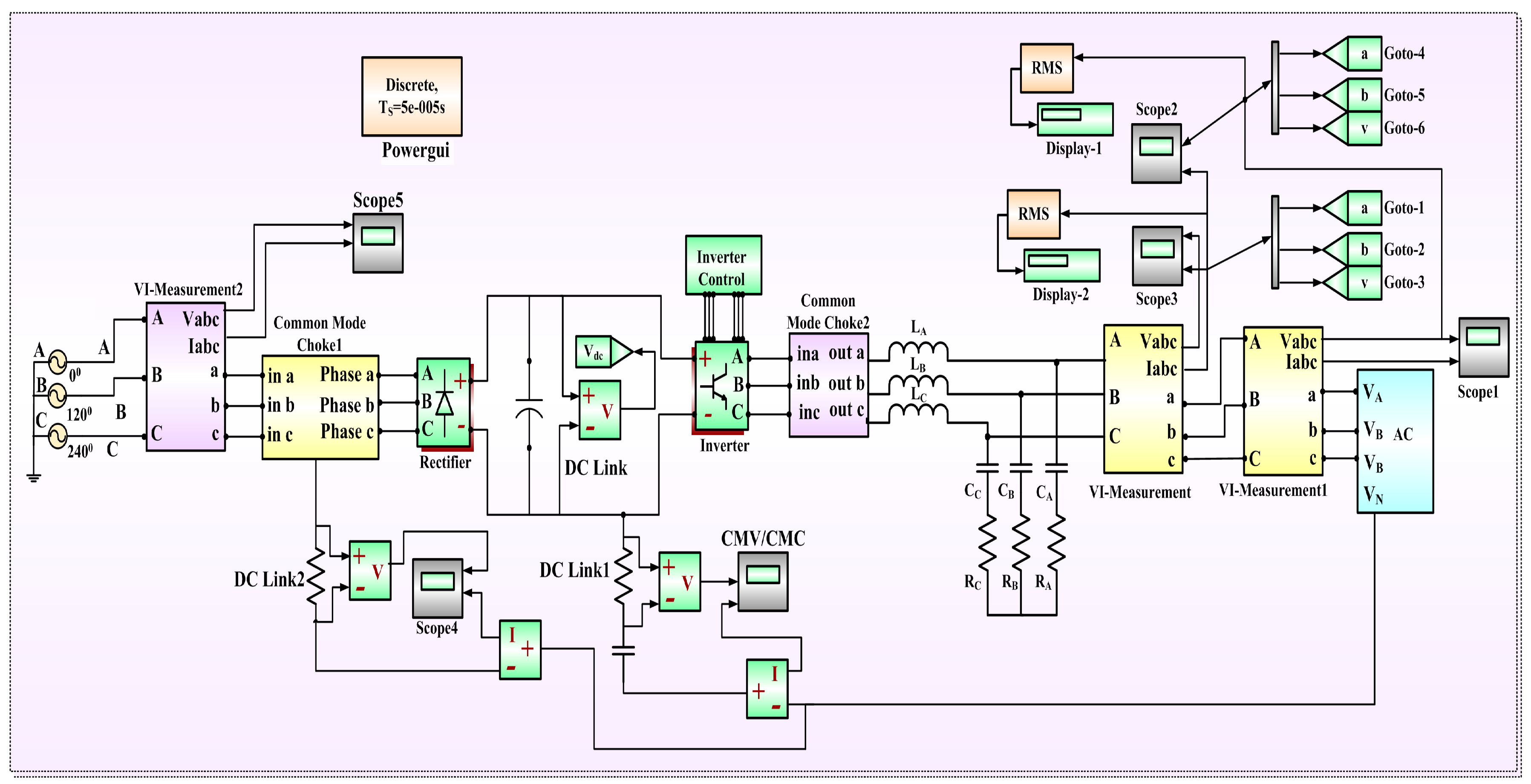
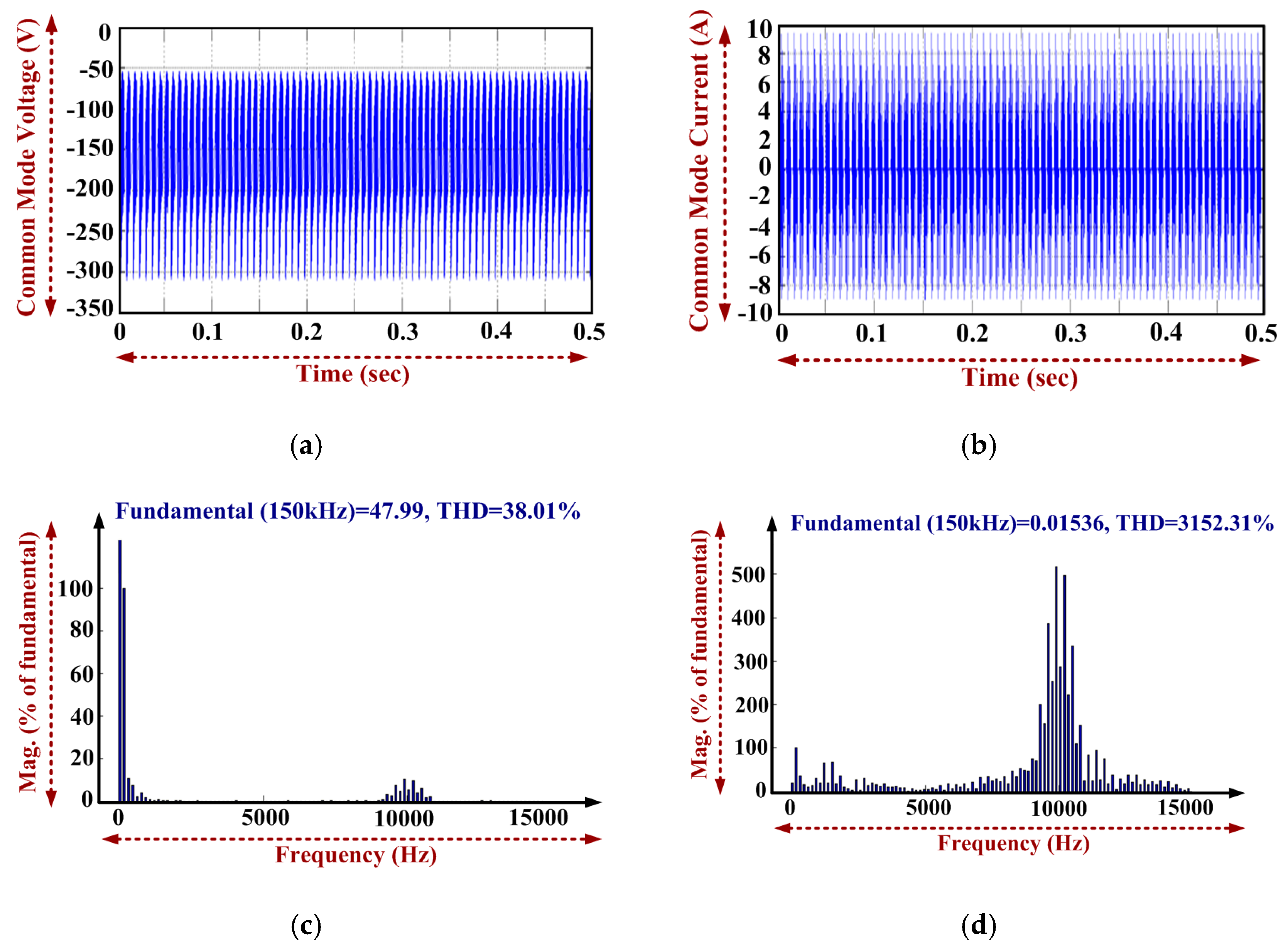
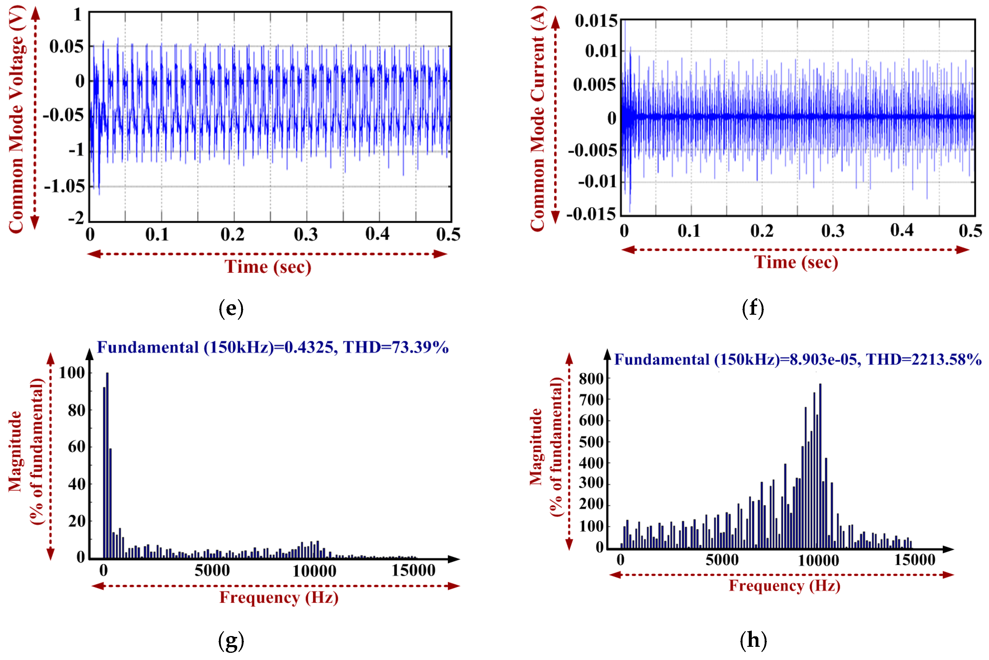
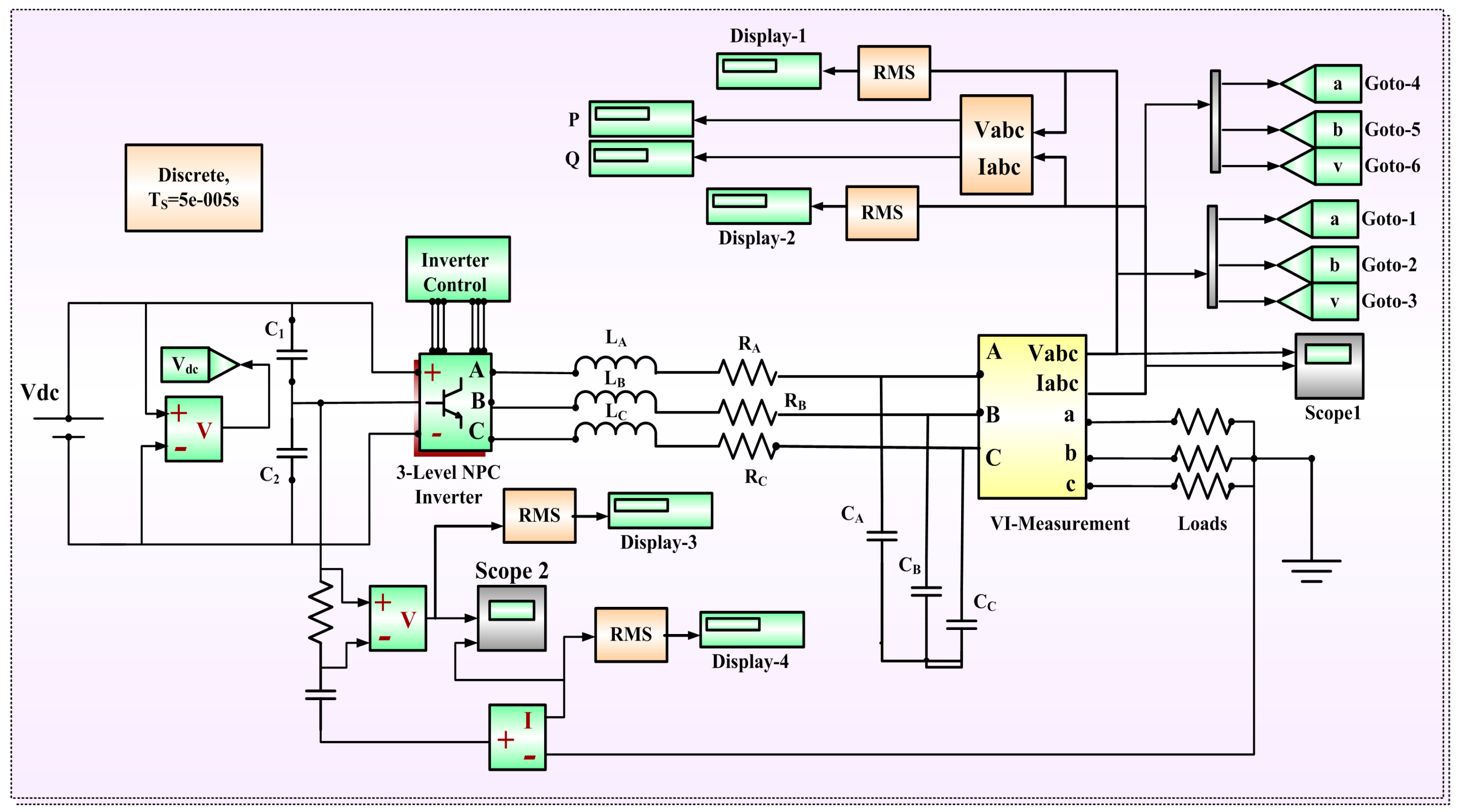
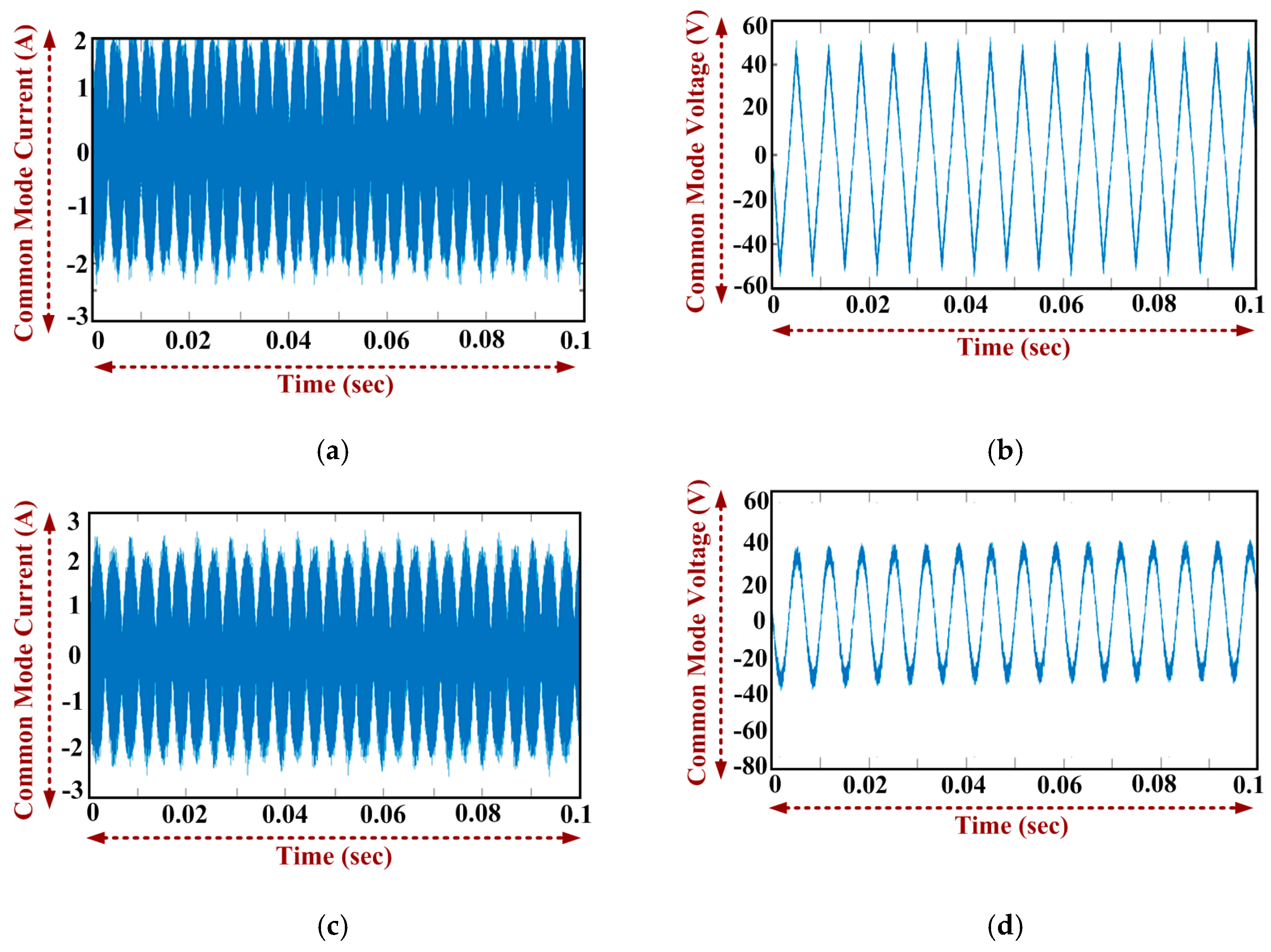
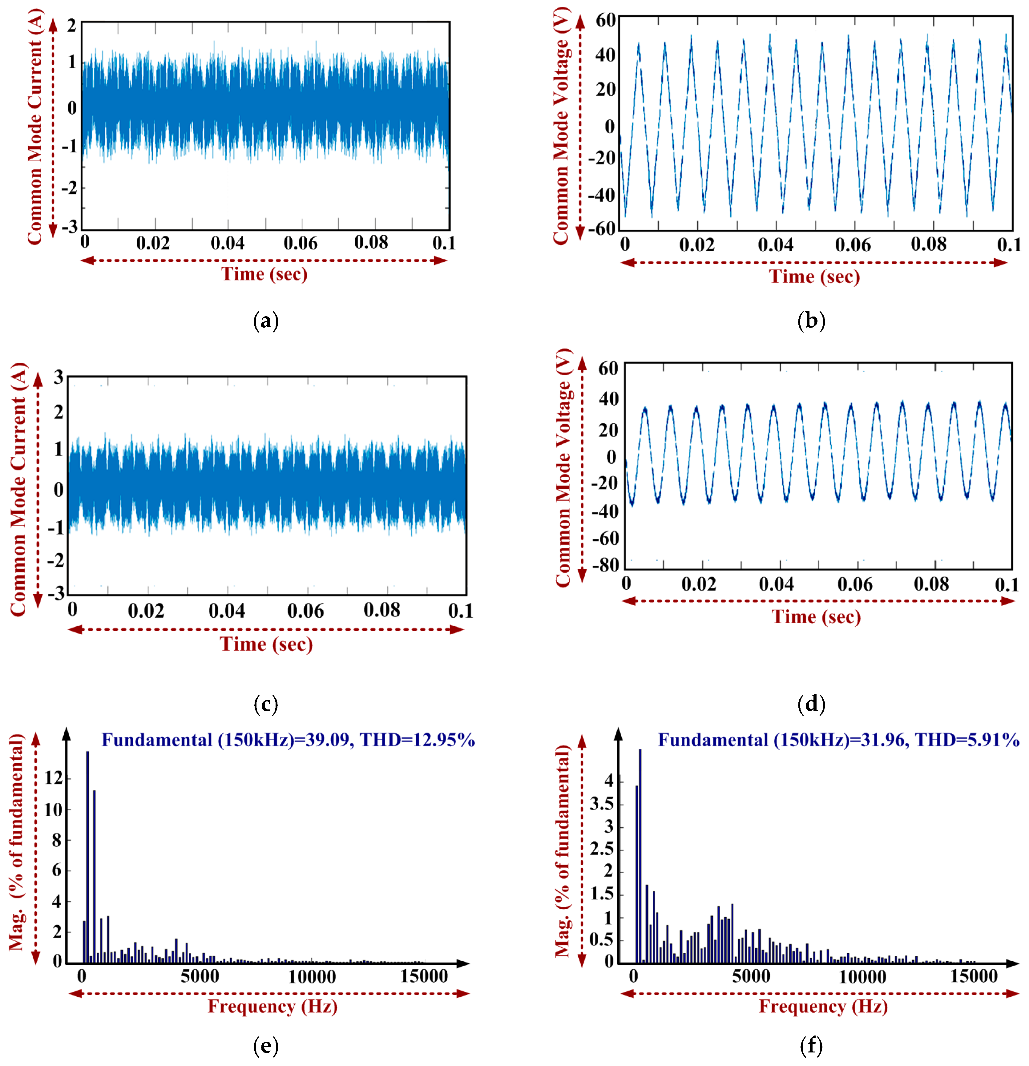
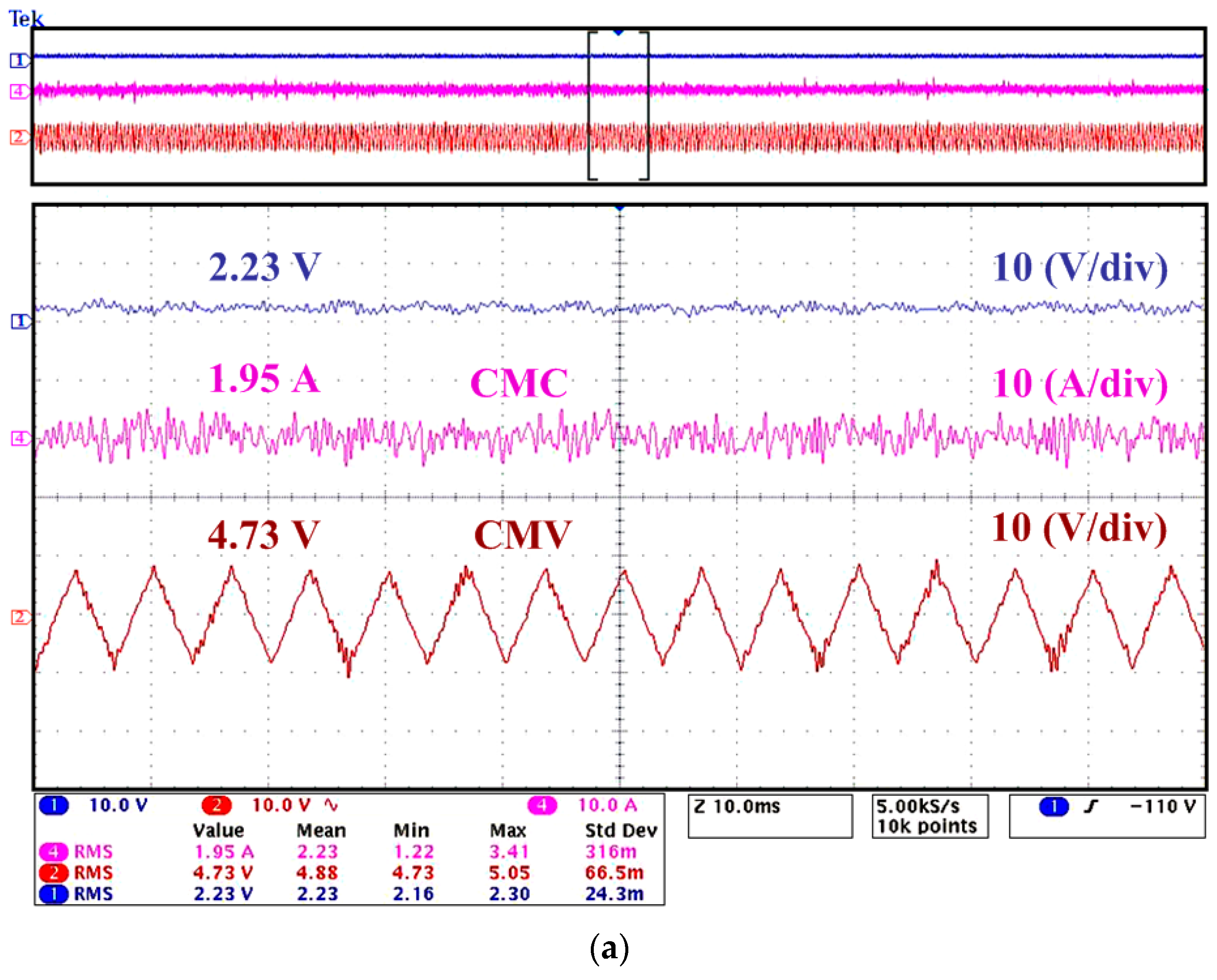
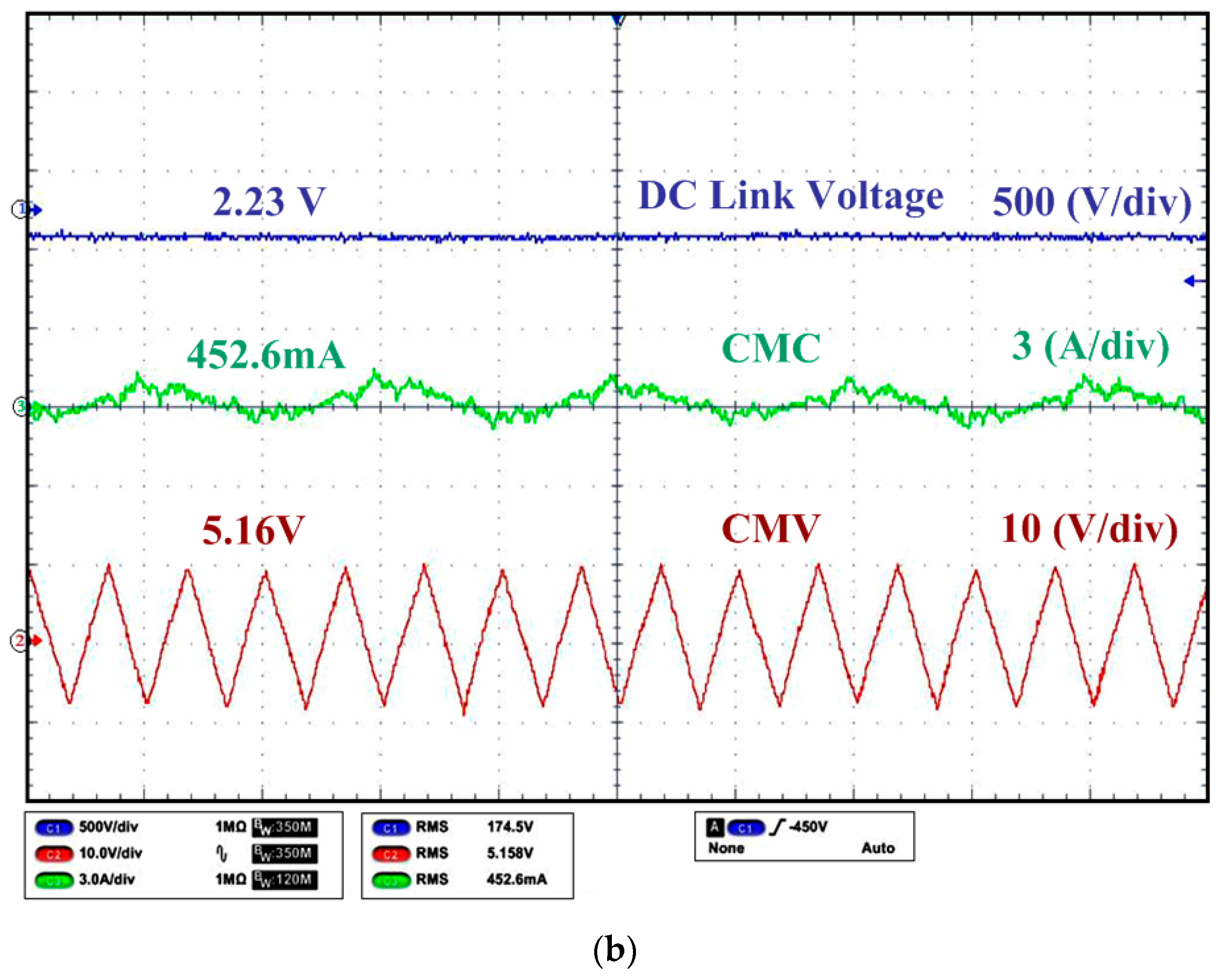
In this paper, EMI mitigation techniques are investigated with the aim to reduce CMV and CMC in a PV-grid tied power inverter. The effect of modulation techniques over CMV and CMC are investigated for two-level and three-level inverters to observe the mitigation of EMI. The modified third harmonic injection method reduced the CMV and CMC by 60% in the system. In order to reduce distortion and to improve the overall efficiency of the system, the modified PWM technique is employed along with EMI chokes.
The article is organized in the seven sections, discussing explicitly the important aspects for investigations and design of EMI filters for the mitigation of CMC and CMV in grid-tied inverter system. In Section 2, the modulation techniques for high power two-level and three-level inverters, are discussed in brief. Section 3 explains the concept of CMV of the inverters and design of filters or EMI chokes. Section 3 also deals with the comparative study of space vector-based and sine-based pulse width modulation (SVPWM and SPWM) techniques. A modified PWM strategy is discussed in Section 4. The results obtained through simulation and experimental works are presented in Section 5. Finally, the conclusion is given in Section 6.

2. Modulation Techniques for High-Power Inverters

Space vector-based and sine wave-based PWM techniques are the common techniques used to generate pulses for the switches of the inverter [29,30]. In the SPWM technique, high-frequency triangular carrier waves (typically several kHz) are compared with the modulating signal (50 Hz or 60 Hz) to generate pulses for a three-phase inverter. In the SVPWM technique, instead of modulating signals, a rotating vector reference is used to generate pulses of the inverter [29,30]. The prime objective of this control and pulse generation scheme is to generate a sinusoidal AC output whose magnitude is limited. The PWM switching scheme not only helps to achieve reduced Total Harmonic Distortion (THD), better harmonic spectrum, and maximum utilization of DC bus but also provides a solution to reduce EMI, switching loss. Figure 1 depicts the power circuitry of three-phase two-level inverter and neutral point clamped (NPC) three-level inverters [21] and its PWM strategies shown in Figure 2, Figure 3, Figure 4 and Figure 5.
The Min–Max modulation strategy is supposed to be equivalent to the space vector modulation strategy. Thus, using this approach, the modulation index can be extended up to 1.15. Figure 2a,b explains the associated waveforms and mathematical model of the reference waveform generation technique through Min–Max modulation strategy, respectively [48]:
o f f s e t   i n   ( V ) = [ max ( V A , V B , V C ) + min ( V A , V B , V C ) 2 ]
where:
{ V A = V m cos ( ω t ) V B = V m cos ( ω t 2 π 3 ) V C = V m cos ( ω t + 2 π 3 )
V r e f = V A + V B + V C + o f f s e t
The reference modulating signals are mathematically defined as follows:
{ V A m = V m cos ( ω t ) + o f f s e t V B m = V m cos ( ω t 2 π 3 ) + o f f s e t V C m = V m cos ( ω t + 2 π 3 ) + o f f s e t
In the third harmonic injection method [52,53], the third harmonic is injected in a modulation scheme to improve the gain of the pulse width modulator in the inverter. Figure 3a,b shows the third harmonic injection modulating signal control reference waveform and mathematical model, respectively.
The reference modulating signals are mathematically defined as follows:
{ V A m = V m cos ( ω t ) + V m 3 cos ( 3 ω t ) V B m = V m cos ( ω t 2 π 3 ) + V m 3 cos ( 3 ω t ) V C m = V m cos ( ω t + 2 π 3 ) + V m 3 cos ( 3 ω t )
In this technique, approximately 17% of third harmonics components are added in the reference waveform of classical SPWM [29,30,34]. The reference waveform of the method third harmonics injection can be also expressed as follows:
f ( ω t ) = ( 1.15 M a × sin ( ω t ) + 0.19 M a × sin ( ω t ) ) ,   0 ω t 2 π
where Ma is the modulation index ratio.

3. Common Mode Voltage

The inverter common mode voltage is calculated by averaging the output voltage (VA, VB, and VC) of each leg as follows [38]:
V C M = V A + V B + V C 3
For the three-phase two-level inverter, the achievable phase output voltage levels could be –VDC/2 or +VDC/2 where VDC is input voltage. If the voltage at the DC link is zero then only the common mode voltage is zero. For the three-level inverter, the achievable phase output voltage levels could be positive, negative, and neutral point voltage. Table 1 and Table 2 tabulated the output vectors and possible common mode voltages for two-level and three-level inverters, respectively.

3.1. Filtering of Common Mode Voltage

The appropriate designed filter circuitry is needed to reduce the common mode voltage. The complete three-phase to grid (AC–DC–AC) system with the connection of a passive filter is shown in Figure 4. The DC link with voltage VD is created between the AC–DC and DC–AC converter and passive filters are added at the input and output side. The filter consists of damping resistance, Y-connected capacitor and common mode chokes. In the given system, a damping resistor RCM2 is connected between grid and neutral point capacitor. Additionally, two chokes, LCM1 and LCM2, and three Y-connected capacitors, CCM2, are connected for filter purposes [12,13,14]. RCM1 and CCM1 are connected between the grid and negative terminal of the DC link. The range of the resonant frequency for the common mode circuitry is about 1.5 kHz [7] and is calculated as follows:
f o = 1 / ( 2 π L C M × C C M )
where LCM and CCM are the equivalent inductance and capacitance values. The practical limitation of the real-time application needs to be considered while designing the capacitors. The capacitor size should be small for the designed frequency in order to reduce the bulkiness of the hardware unit.

3.2. Comparison of SPWM and Space Vector PWM Techniques for a Two-Level Inverter at a Higher Switching Frequency

The simple open-loop analysis is carried out for a two-level inverter for current and voltage distortions both with and without a filter. For the analysis, the modulation index is maintained at 0.8 and taken over a range of frequencies between 1 kHz and 150 kHz and the obtained results are tabulated in Table 3. After comparing SPWM and SVPWM results, it is known that SVPWM provides superior results for two-level inverter system. For reduction in CMV, the SVPWM technique provides the best results; however, due to tedious calculations, the requirement of high-end processors and complex hardware implementation, space vector modulation can be replaced with the carrier-based modulation strategy which will give the same results as that of the space vector modulation technique. If the reduction in the CMC can be achieved by using such a modulation strategy, the size of the common mode choke can be reduced.

4. Modified PWM Schemes

Among discussed PWM schemes, SVPWM provides quality results [30]. Nevertheless, due to some inherent disadvantages, the space vector modulation strategy is ruled out from the agenda. Thus. the next challenge was to obtain similar results, which were given by the space vector modulation, in carrier-based modulation as well. The modified carrier phase shift scheme is developed based on the concept of phase disposition PWM scheme. It is given that the input voltage is balanced and the possible two conditions are:
  • One input phase voltage is negative and two input phase voltage is positive.
  • One input phase voltage is positive and two input phase voltage is positive.
V A + V B + V C = 1
It is considered that 0 < VA, 0 > VB, and 0 > VC and CMV are caused with the peak value to reach a higher voltage level than 1/6 × VDC. The carrier signals and output voltage reference relation for the switching 0–1–1 is as follows:
As phase disposition PWM (PDPWM) is used, at any point of time:
f o r   t h e   s t a t e   0 1 1 { V C a r r i e r A V C a r r i e r B = 1 3 × V C a r r i e r A 2 > 0
Hence, to avoid this state, 3 × V C a r r i e r A 2 < 0 , this condition is to be satisfied. This is done by using three carrier waves, which are 120° apart from each other. Figure 5 shows the waveform associated with PWM strategies. Figure 5a depicts the associated waveform of the PDPWM method where the max amplitude of the addition of the carrier waves is 2 (see amplitude in (3) in Figure 5a). Figure 5b depicts the associated waveform of the modified PWM method where the max amplitude of the addition of the carrier waves is around 1.5 (see amplitude in (4) in Figure 5b).

5. Simulation and Experimental Results

The simulation results are presented for the complete AC–DC–AC system. The circuit-level model was developed using the Simulink platform. The closed-loop analysis of both two-level and three-level inverters is carried out. The specifications of the system parameters are given in Appendix A.

5.1. Closed-Loop Analysis of the Two-Level Inverter

The model of the system is done in various stages. Figure 6 shows the complete closed-loop AC–DC–AC system Simulink model with the two-level inverter. The first section includes the diode rectifier model to obtain a constant DC voltage. Then the DC link capacitor was designed so as to provide a constant DC input voltage to the three-phase two-level inverter circuit which is modelled using Insulated Gate Bipolar Transistor (IGBTs) and SVPWM techniques were implemented for firing the inverter circuit.
The analysis of CMV and CMC for the given system is done without filter implementation and the achieved results are depicted in Figure 7a–d. The Fast Fourier Transform(FFT) analysis of the CMV and CMC waveform (150 kHz component) are done without filter, and it is observed that THD of the CMV and CMC is 38.01% and 3152.31%, respectively. The analysis of the common mode voltage and current for the given system are done with a filter implementation and the achieved results are depicted in Figure 7e–h. The FFT analysis of the CMV and CMC waveform (150 kHz component) are done with a filter and it is observed that the THD of the CMV and CMC is 73.39% and 2213.58%, respectively.
From the investigation, the objective of reducing the CMC and CMV of the two-level inverter is achieved. From the analysis made, it can be concluded that when the two-level inverter is operating at a frequency above 10 kHz, the EMI increases drastically. Additionally, the CMV and CMC of the system cannot be reduced effectively by changing the reference, instead the size of the EMI filters have to be larger. Therefore, we need to consider the three-level inverter analysis.

5.2. Closed-Loop Analysis of the Three-Level Inverter

Based on the earlier explanation, the Simulink model of the three-level NPC system is designed in MATLAB. Figure 8 shows the Simulink model of the designed three-level NPC system.

5.2.1. Existing PWM Method

Using Min–Max and the third harmonic injection method, the common mode current and voltage are investigated for the three-level NPC inverter. Figure 9a–d depicts the waveforms of CMC using existing Min–Max method, CMV using existing Min–Max method, CMC using the existing third harmonic injection methods, and CMV using the existing third harmonic injection method, respectively.
The fast Fourier transform (FFT) is conducted for Min–Max and third harmonic injection PWM techniques and it is observed that common mode voltage THD is 14.74% for Min–Max strategy and 11.60% for the third harmonic injection method. In the existing PWM method, the magnitude of the common mode current (rms value) is 1.191 A using the Min–Max and 1.199 A in the case of the third harmonic injection method. This can be reduced further by using Modified PWM Technique.

5.2.2. Modified PWM Method

The simulation results for the modified Min–Max method and third harmonic injection methods as applied in the three-level NPC inverter. Figure 10a–d obtained waveform of CMC using modified Min–Max method, waveform CMV using modified Min–Max method, waveform of CMC using modified third harmonic injection methods, and waveform of CMV using modified third harmonic injection methods, respectively. Figure 10e,f show the FFT analysis of CMV and CMC with filter, respectively. It is observed that the THD of the CMV and CMC are 12.95% and 5.91%, respectively. Before modifying the PWM scheme, the common mode voltage and current of the inverter are experimentally investigated and shown in Figure 11a. Without modification, the RMS values of the common mode current and common mode voltage are 1.95 A and 4.73 V, respectively.
After modifying the PWM scheme, the common mode voltage and current of the inverter are experimentally investigated and shown in Figure 11b. After modification, the RMS values of the common mode current and common mode voltage are 452.6 mA and 5.16 V, respectively. In Table 4, the observed results are tabulated and it is clear that, after modifying the PWM method, the common mode current is reduced significantly with a small increment in the common mode voltage.
In Table 5, a comparison of PWM strategies for reduction in CMC, CMV, and voltage THD of the three-level inverter is tabulated based on the obtained results. The simulated results show that when the modified PWM method is implemented there is a considerable reduction in CMC. The voltage THD of the system is also observed to be reduced considerably. This satisfies the objective of optimizing the PWM technique to reduce the CMV and current in grid-tied inverters. From the above comparison, it is clear that the modified third harmonic injection approach shows a significant amount of reduction in the CMV and CMC. EMI mitigation techniques are investigated with the aim to reduce the CM voltage and current in PV grid-tied power inverters. The common mode undesirable effects for grid-tied inverter systems has been discussed and compared for different PWM schemes. Two small passive filters are connected between the rectifier input and grid neutral point, and in between the grid and output port of the inverter and tested for a three-phase two-level inverter using a passive cancellation method.

6. Conclusions

In order to reduce distortion in the system, the modified PWM technique is employed along with EMI chokes. Various PWM strategies are analyzed to reduce the CMV and CMC, and a modified PWM approach is presented for a three-phase three-level inverter. The modified third harmonic injection method reduced the CMC by 60% in the system with a tradeoff to CMV. Simulation and experimental results are provided which show good agreement with each other and validate that the control strategies with different PWM techniques are valuable, optimize the output parameters, and are effective in preventing common mode undesirable effects along with and without filters. Hence, it is economic to use modified techniques so that the filter size can be reduced and the final product will be lightweight with a reduced cost compared with conventional strategies and existing PWM techniques.

Author Contributions

All authors were involved in developing the concept to make the article an error-free technical outcome for the set investigation work

Funding

This research received no external funding.

Acknowledgments

The authors would like to express their sincere gratitude to the Renewable Energy Lab, College of Engineering, Prince Sultan University, Riyadh, Saudi Arabia for giving the opportunity to execute the project in this area.

Conflicts of Interest

The authors declare no conflict of interest.

Nomenclature

CMCommon mode
CMCCommon mode current
CMVCommon mode voltage
DCDirect current
ACAlternating current
EMIElectromagnetic interference
PWMPulse width modulation
PVPhotovoltaic
VFDVariable frequency drive
dv/dtChange in voltage
di/dtChange in current
LCProduct of inductance and capacitance
SPWMSinewave pulse width modulation
NPCNeutral point clamped
SVPWMSpace vector pulse width modulation
PDPWMPhase disposition PWM
SSSpread spectrum
VA, VB, VCAC voltage of each leg
VRefVoltage of reference modulating signal
VAm, VBm, VCmVoltage of reference modulating signal for each leg
VmPeak value of output voltage
Vm3Peak value of third harmonic of output voltage
f(wt)Function of reference waveform of the method third harmonics injection
VdcDC input voltage
RCM1, RCM2Damping resistor
LCM1, LCM2Chokes
CCM1, CCM2Capacitor
LCM, CCMCommon mode equivalent inductance and capacitor
foCommon mode resonant frequency

Appendix A

Table A1. Specifications of the system parameters.
Name of the ComponentRating
DC link voltage560 V
DC link capacitor2200 µF
Filter inductance450 mH
Filter capacitance11.6 µF
Rated phase voltage230 V
Frequency50 Hz
Grid Parameters
Grid voltage and frequency230 V, 50 Hz
Carrier frequency20 kHz

References

  1. Kerekes, T.; Teodorescu, R.; Liserre, M. Common mode voltage in case of transformerless PV inverters connected to the grid. In Proceedings of the IEEE International Symposium on Industrial Electronics, Cambridge, UK, 30 June–2 July 2008; pp. 2390–2395. [Google Scholar]
  2. Esmaeli, A.; Tavassoli, F. A novel passive filter to reduce PWM inverters adverse effects in electrical machine system. World App. Sci. J. 2011, 13, 2536–2544. [Google Scholar]
  3. Elnady, A.; Salama, M.M.A. Unified approach for mitigating voltage sag and voltage flicker using the DSTATCOM. In Proceedings of the IEEE Power Engineering. Society General Meeting, Denver, CO, USA, 6–10 June 2004; p. 645. [Google Scholar]
  4. Yao, Z.; Xiao, L. Control of single-phase grid-connected inverters with nonlinear loads. IEEE Trans. Ind. Electron. 2011, 60, 1384–1389. [Google Scholar] [CrossRef]
  5. Prasad, K.N.V.; Kumar, G.R.; Kumar, Y.S.A.; Narayana, G.S. In Proceedings of the IEEE International Conference on Computer Communication and Informatics, Coimbatore, India, 4–6 January 2013; pp. 1–6.
  6. Khan, S.A.; Guo, Y.; Zhu, J. A high efficiency transformerless PV grid-connected inverter with leakage current suppression. In Proceedings of the 9th International Conference on Electrical and Computer Engineering, Dhaka, Bangladesh, 20–22 December 2016; pp. 190–193. [Google Scholar]
  7. Grishanov, E.V.; Brovanov, S.V. Aspects of common-mode leakage current suppression in single-phase PV-generation systems. In Proceedings of the 18th International Conference of Young Specialists on Micro/Nanotechnologies and Electron Devices, Erlagol, Russia, 29 June–3 July 2017; pp. 541–546. [Google Scholar]
  8. Zhu, H.; Liu, D.; Chen, H.; Chen, G. An improved foster model of common-mode inductor and its application in EMI filter design. In Proceedings of the IEEE International Symposium on Electromagnetic Compatibility and Asia-Pacific Symposium on Electromagnetic Compatibility, Singapore, 14–18 May 2018; 461–465. [Google Scholar]
  9. Zhang, L.; Sun, K.; Xing, Y.; Xing, M. H6 transformerless full-bridge PV grid-tied inverters. IEEE Trans. Power Electron. 2013, 29, 1229–1238. [Google Scholar] [CrossRef]
  10. Aggeler, D.; Canales, F.; Biela, J.; Kolar, J.W. Dv/Dt-control methods for the SiC JFET/Si MOSFET cascode. IEEE Trans. Power Electron. 2013, 28, 4074–4082. [Google Scholar] [CrossRef]
  11. Kakosimos, P.; Sarigiannidis, A.; Beniakar, M.; Kladas, A. Investigation of transformerless topologies for renewable energy applications eliminating leakage currents. In Proceedings of the MedPower 2014, Athens, Greece, 2–5 November 2014; pp. 1–5. [Google Scholar]
  12. Araujo, S.V.; Zacharias, P.; Mallwitz, R. Highly efficient single-phase transformerless inverters for grid-connected photovoltaic systems. IEEE Trans. Ind. Electron. 2010, 57, 3118–3128. [Google Scholar] [CrossRef]
  13. Figueredo, R.S.; Carvalho, K.C.M.; Ama, N.R.N.; Matakas, L. Leakage current minimization techniques for single-phase transformerless grid-connected PV inverters–An overview. In Proceedings of the Brazilian Power Electronics Conference, Gramado, Brazil, 27–31 October 2013; pp. 517–524. [Google Scholar]
  14. Zografos, D.; Koutroulis, E.; Yang, Y.; Blaabjerg, F. Minimization of leakage ground current in transformerless single-phase full-bridge photovoltaic inverters. In Proceedings of the 17th European Conference on Power Electronics and Applications, Geneva, Switzerland, 8–10 September 2015; pp. 1–10. [Google Scholar]
  15. Yang, B.; Li, W.; Gu, Y.; Cui, W.; He, X. Improved transformerless inverter with common-mode leakage current elimination for a photovoltaic grid-connected power system. IEEE Trans. Power Electron. 2012, 27, 752–762. [Google Scholar] [CrossRef]
  16. Liu, D.; Zhu, H.; Zhao, R. Novel common-mode current suppression method in transformerless PV grid-connected system. Appl. Sci. 2018, 8, 2072. [Google Scholar] [CrossRef]
  17. Yang, Y.; Mao, C.; Wang, D.; Tian, J.; Yang, M. Modeling and analysis of the common mode voltage in a cascaded H-bridge electronic power transformer. Energies 2017, 10, 1357. [Google Scholar] [CrossRef]
  18. Yang, T.; Hao, X.; He, R.; Wei, Z.; Huang, T.; Zhang, Y. Hybrid modulation strategy to eliminate current distortion for PV GRID-tied H6 inverter. Appl. Sci. 2018, 8, 2578. [Google Scholar] [CrossRef]
  19. Swain, S.D.; Ray, P.K.; Mohanty, K.B. Improvement of power quality using a robust hybrid series active power filter. IEEE Trans. Power Electron. 2017, 32, 3490–3498. [Google Scholar] [CrossRef]
  20. Hashempour, M.M.; Savaghebi, M.; Vasquez, J.C.; Guerrero, J.M. A control architecture to coordinate distributed generators and active power filters coexisting in a microgrid. IEEE Trans. Smart Grid 2016, 7, 2325–2336. [Google Scholar] [CrossRef]
  21. Singh, B.; Jain, C.; Goel, S.; Gogia, R.; Subramaniam, U. A sustainable solar photovoltaic energy system interfaced with grid-tied voltage source converter for power quality improvement. Electr. Power Compon. Syst. 2016, 45, 171–183. [Google Scholar] [CrossRef]
  22. Wong, M.C.; Dai, N.Y.; Lam, C.S. Parallel Power Electronics Filters in Three-Phase Four-Wire Systems: Principle, Control and Design; Springer: Berlin, Germany, 2016; pp. 59–165. [Google Scholar]
  23. Sarajian, S. Design and control of grid interfaced voltage source inverter with output LCL Filter. Int. J. Electron. Commun. Electr. Eng. 2014, 4, 26–40. [Google Scholar]
  24. Nazeri, A.A. Comparison of different filter types for grid connected inverter. In Proceedings of the 29th PIERS Proceedings, Marrakesh, Marocco, 20–23 March 2011. [Google Scholar]
  25. Boonpirom, N. The EMI improvement on active filter using common-mode noise circuits balanced method. In Proceedings of the 18th International Conference on Electrical Machines and Systems, Pattaya, Thailand, 25–28 October 2015; pp. 1325–1328. [Google Scholar]
  26. Chen, X.; Xu, D.; Liu, F.; Zhang, J. A novel inverter-output passive filter for reducing both differential- and common-mode dv/dt at the motor terminals in PWM drive systems. IEEE Trans. Ind. Electron. 2007, 54, 419–426. [Google Scholar] [CrossRef]
  27. Kim, H.; Lee, H.; Sul, S. A new PWM strategy for common-mode voltage reduction in neutral point clamped inverter-fed AC motor drives. IEEE Trans. Ind. Appl. 2001, 37, 1840–1845. [Google Scholar]
  28. Gupta, A.K.; Khambadkone, A.M. A space vector modulation scheme to reduce common mode voltage for cascaded multilevel inverters. IEEE Trans. Power Electron. 2007, 22, 1672–1681. [Google Scholar] [CrossRef]
  29. Babu, B.C. Control of Voltage Source Inverters Using PWM/SVPWM for Adjustable Speed Drive Applications. Ph.D. Thesis, Department of Electrical Engineering, National Institute of Technology Rourkela, Rourkel, India, May 2009. [Google Scholar]
  30. Kumar, K.V.; Michael, P.A.; John, J.P.; Kumar, D.S.S. Simulation and comparison of SPWM and SVPWM control for three phase inverter. ARPN J. Eng. Appl. Sci. 2010, 5, 61–74. [Google Scholar]
  31. Mehrasa, M.; Pouresmaeil, E.; Zabihi, S.; Trujillo Caballero, J.C.; Catalão, J.P.S. A novel modulation function-based control of modular multilevel converters for high voltage direct current transmission systems. Energies 2016, 9, 867. [Google Scholar] [CrossRef]
  32. Moranchel, M.; Huerta, F.; Sanz, I.; Bueno, E.; Rodríguez, F.J. A comparison of modulation techniques for modular multilevel converters. Energies 2016, 9, 1091. [Google Scholar] [CrossRef]
  33. Jerin, A.R.A.; Palanisamy, K.; Umashankar, S.; Sanjeevikumar, P. Comparative analysis of feed-forward and synchronous reference frame control-based dynamic voltage restorer. Adv. Power Syst. Energy Manag. 2018, 411–420. [Google Scholar] [CrossRef]
  34. Tang, X.; Lai, C.; Liu, Z.; Zhang, M. A SVPWM to eliminate common-mode voltage for multilevel inverters. Energies 2017, 10, 715. [Google Scholar] [CrossRef]
  35. Pareschi, F.; Rovatti, R.; Setti, G. EMI reduction via spread spectrum in DC/DC converters: State of the art, optimization, and tradeoffs. IEEE Access 2015, 3, 2857–2874. [Google Scholar] [CrossRef]
  36. Park, H.; Kim, M.; Jung, J. Spread spectrum technique to reduce EMI emission for an LLC resonant converter using a hybrid modulation method. IEEE Trans. Power Electron. 2018, 33, 3717–3721. [Google Scholar] [CrossRef]
  37. Kato, T.; Inoue, K.; Akimasa, K. EMI reduction method for a Single-Phase PWM inverter by suppressing common-mode currents with complementary switching. In Proceedings of the IEEE 5th International Power Electron and Motion Control Conference, Shanghai, China, 14–16 August 2006; pp. 1–5. [Google Scholar]
  38. Morris, C.T.; Han, D.; Sarlioglu, B. Reduction of common mode voltage and conducted EMI through three-phase inverter topology. IEEE Trans. Power Electron. 2017, 32, 1720–1724. [Google Scholar] [CrossRef]
  39. Perotti, M.; Fiori, F. Software based control of the EMI generated in BLDC motor drives. In Proceedings of the International Symposium on Electromagnetic Compatibility-EMC EUROPE, Wroclaw, Poland, 5–9 September 2016; pp. 417–421. [Google Scholar]
  40. Perotti, M.; Fiori, F. Investigating the EMI mitigation in power inverters using delay compensation. IEEE Trans. Power Electron. 2019, 34, 4270–4278. [Google Scholar] [CrossRef]
  41. Hedayati, M.H.; Acharya, A.B.; John, V. Common-mode filter design for PWM Rectifier-based motor drives. IEEE Trans. Power Electron. 2013, 28, 5364–5371. [Google Scholar] [CrossRef]
  42. Ali, M.; Labouré, E.; Costa, F.; Revol, B. Design of a hybrid integrated EMC Filter for a DC–DC power converter. IEEE Trans. Power Electron 2012, 27, 4380–4390. [Google Scholar] [CrossRef]
  43. Yücel, A.C.; Bağcı, H.; Michielssen, E. An adaptive multi-element probabilistic collocation method for statistical EMC/EMI characterization. IEEE Trans. Electromagn. Comp. 2013, 55, 1154–1168. [Google Scholar] [CrossRef]
  44. Yazdani, M.R.; Farzanehfard, H. Conducted electromagnetic interference analysis and mitigation using zero-current transition soft switching and spread spectrum techniques. IET Power Electron. 2012, 5, 1034–1041. [Google Scholar] [CrossRef]
  45. Kovačević, I.F.; Friedli, T.; Muesing, A.M.; Kolar, J.W. 3-D electromagnetic modeling of EMI input filters. IEEE Trans. Ind. Electron. 2014, 61, 231–242. [Google Scholar] [CrossRef]
  46. Son, Y.C.; Sul, S. A new active common-mode EMI filter for PWM inverter. IEEE Trans. Power Electron. 2003, 18, 1309–1314. [Google Scholar] [CrossRef]
  47. Xing, L.; Sun, J. Conducted common-mode EMI reduction by impedance balancing. IEEE Trans. Power Electron. 2012, 27, 1084–1089. [Google Scholar] [CrossRef]
  48. Salamah, A.M.; Finney, S.J.; Williams, B.W. Three-phase phase-lock loop for distorted utilities. IET Electric. Power Appl. 2007, 1, 937–945. [Google Scholar] [CrossRef]
  49. Morris, C.T.; Han, D.; Sarlioglu, B. Comparison and evaluation of common mode EMI filter topologies for GaN-based motor drive systems. In Proceedings of the IEEE Applied Power Electronics Conference and Exposition, Long Beach, CA, USA, 20–24 March 2016; pp. 2950–2956. [Google Scholar]
  50. Ogasawara, S.; Ayano, H.; Akagi, H. An active circuit for cancellation of common-mode voltage generated by a PWM inverter. IEEE Trans. Power Electron. 1998, 13, 835–841. [Google Scholar] [CrossRef] [Green Version]
  51. Alam, A.; Mukul, M.K.; Thakura, P. Wavelet transform-based EMI noise mitigation in power converter topologies. IEEE Trans. Electromagn. Compat. 2016, 58, 1662–1673. [Google Scholar] [CrossRef]
  52. Tamasas, M.E.; Saleh, M.; Shaker, M.; Hammoda, A. Comparison of different third harmonic injected PWM strategies for 5-level diode clamped inverter. In Proceedings of the IEEE Power and Energy Conference at Illinois, Champaign, IL, USA, 23–24 February 2017; pp. 1–6. [Google Scholar]
  53. Colak, I.; Bayindir, R.; Kabalci, E. A modified harmonic mitigation analysis using Third Harmonic Injection PWM in a multilevel inverter control. In Proceedings of the 14th International Power Electronics and Motion Control Conference, Ohrid, Macedonia, 6–8 September 2010; pp. 215–220. [Google Scholar]
Figure 1. Power circuitries of (a) three-phase two-level inverter, and (b) neutral point clamped (NPC) three-level inverter.
Energies 12 03395 g001
Figure 2. Reference generation through Min–Max modulation strategy (a) associate waveform, and (b) mathematical model.
Energies 12 03395 g002
Figure 3. Modulating signal of third harmonic injection control technique (a) modulating signal, and (b) mathematical model.
Energies 12 03395 g003
Figure 4. Complete three-phase to grid (AC–DC–AC) system with the connection of a passive filter.
Energies 12 03395 g004
Figure 5. Waveform associated with PWM strategies (a) PDPWM method, max amplitude of the addition of the carrier waves is 2, (b) modified PWM method, max. amplitude of the addition of the carrier waves is around 1.5.
Energies 12 03395 g005
Figure 6. Complete closed-loop AC–DC–AC system Simulink model with the two-level inverter.
Energies 12 03395 g006
Figure 7. Simulation results: (a) CMV without filter; (b) CMC without filter; (c) without filter, common mode voltage FFT analysis; (d) without filter, common mode current FFT analysis; (e) CMV with filter; (f) CMC with filter; (g) with filter, common mode voltage FFT analysis; (h) with filter, common mode current FFT analysis.
Energies 12 03395 g007aEnergies 12 03395 g007b
Figure 8. Matlab/Simulation model of the three-phase three-level NPC inverter.
Energies 12 03395 g008
Figure 9. Simulation results: (a) CMC using existing Min–Max method; (b) CMV using existing Min–Max method; (c) CMC using the existing third-harmonic injection method; (d) CMV using the existing third-harmonic injection method.
Energies 12 03395 g009
Figure 10. Simulation results: (a) CMC using the modified Min–Max method; (b) CMV using the modified Min–Max method; (c) CMC using the modified third-harmonic injection method; (d) CMV using the modified third-harmonic injection method; (e) with filter, common mode voltage FFT analysis; (f) with filter, common mode current FFT analysis.
Energies 12 03395 g010
Figure 11. Experimental results: common mode current and common mode voltage, (a) before modifying the PWM strategy, and (b) after modifying the PWM strategy.
Energies 12 03395 g011aEnergies 12 03395 g011b
Table 1. Output vectors and common-mode voltages for two-level inverter.
Output Vector (VA, VB, VC)CMV (VCM)
(+ + +)(1/2) × VDC
(+ + −), (+ − +), (− + +)(1/6) × VDC
(+ − −), (− + −), (− − +)(1/6) × VDC
(− − −)(1/2) × VDC
(+ + +)(1/2) × VDC
(+ + −), (+ − +), (− + +)(1/6) × VDC
Table 2. Output vectors and common-mode voltages for three-level NPC inverter.
Output Vector (VA, VB, VC)CMV (VCM)
(+ + +)(1/2) × VDC
(+ + 0), (+ 0 +),(0 + +)(1/3) × VDC
(+ + −), (+ − +), (− + +), (+ 0 0), (0 + 0), (0 0 +)(1/6) × VDC
(+ - 0), (+ 0 −), (− + 0), (0 + −), (− + 0), (0 − +), (0 0 0)0
(+ − −), (− + −), (− − +), (− 0 0), (0 − 0), (0 0 −)(1/6) × VDC
(− − 0), (− 0 −), (0 − −)(1/3) × VDC
(− − −)(1/2) × VDC
Table 3. THD comparison of SPWM and SVPWMM techniques.
Switching TechniqueSwitching FrequencyWithout Filter (THD%)With Filter (THD%)
Line Current (A)Line Voltage (V)Line Current (A)Line Voltage (V)
SPWM1 kHz64.81138.22.536.88
10 kHz24.988.461.044.16
50 kHz24.2767.921.034.12
100 kHz24.2767.921.034.12
120 kHz31.39106.823.865.63
150 kHz43.95301.927.427.89
SVPWM1 kHz4.8252.840.140.66
10 kHz3.1543.890.110.42
50 kHz3.1543.890.110.43
100 kHz8.7431.840.361.47
150 kHz5.7556.330.451.03
Table 4. Experimental results.
Experimental TestCMV (V)CMC (A)
Before applying modified PWM4.73 V1.95 A
After applying Modified PWM5.16 V452.6 mA
Table 5. Comparison of PWM strategies for reduction in the CMC, CMV, and voltage THD of the three-level inverter.
Modulation TechniqueCMV (V)CMC (A)Voltage THD (%)
Existing PWM Strategy
Min–Max34.71.86314.27
Third Harmonic Injection34.71.86311.5
Modified PWM Strategy
Modified Min–Max43.310.7412.95
Modified Third Harmonic Injection34.840.745.77

