1. Introduction
Currently, small-signal modeling of DC/DC converters with linear feedback control is a mature method [
1]. The model of a DC/DC converter using this method has three independent input variables, of which the duty cycle,
is a control input variable and both the DC power supply voltage,
, and the load current,
, are disturbance input variables (variables marked with “^” are small-signal perturbation ac variables). The open-loop output voltage,
, can be expressed as
, where both
Gvd(
s) and
Gvi(
s) are linear transfer functions. However, one or more product terms exist in averaged equations for converters. A small-signal model of a converter is constructed by perturbing and linearizing its large-signal about a certain steady-state operating point. The nonlinear product terms are ignored, thereby requiring that the magnitude of small ac variables be much smaller than the steady-state dc values and that the modulation frequency be much lower than the switching frequency. When designing a feedback controller, it is often necessary to ignore disturbance inputs and treat the system as a single-input single-output system. Consequently, the designed controller has a large margin, and the performance of the system cannot be guaranteed upon large-signal disturbances such as sudden load changes and power supply fluctuations. Furthermore, when the output capacitor voltage is used as an output variable, the small-signal disturbance models of voltage-boosting DC/DC converters have zeros on the right half of the complex plane [
2] and are non-minimum phase (NMP) systems. NMP zeros can cause undershoots and oscillations in a step response [
3]. If the controller is designed using linear system theory, the way to handle the NMP problem is usually to limit the system bandwidth to avoid the influence of the NMP characteristic on the system’s stability. However, due to the low bandwidth, the speed and robustness of the system’s dynamic response are limited.
With the development of new-energy distributed DC power supply systems, DC/DC converters must meet the requirements of intermittent and random energy conversions and will always operate in a non-steady state at dynamically changing operating points. The small-signal assumptions are no longer applicable. Additionally, a distributed power supply system often contains multiple power sources, and there are major changes in the way that DC/DC converters are connected, bringing the following new challenges to control system design. (1) The variable coupling problem of multiport integrated DC/DC converters [
4,
5,
6,
7,
8]. Because of the presence of multiple power sources or loads, the control system of a multiport integrated converter is often composed of multiple closed voltage and current loops. These closed loops share the same output filter, resulting in coupling occurring between the closed loops. Thus, the coupling factor cannot be ignored when designing control systems. (2) The nonlinear load problem of cascaded DC/DC converters. The second-stage converter can often be treated as a constant power load (CPL) on the first-stage converter. Because of its negative impedance, the CPL will affect the stability of the cascaded system [
9,
10]. In summary, DC/DC converters in distributed power supply systems have varied and complex inputs and loads. Large-signal modeling should be adopted to fully describe the nonlinear characteristics of systems, and the problems of decoupling, should be addressed.
To date, multiple large-signal modeling methods have been formulated [
11,
12,
13,
14]. Large-signal models of DC/DC converters are often nonlinear, and system analysis and synthesis require nonlinear control theory such as feedback linearization, Lyapunov control, sliding-mode control, passivity-based control, and optimal control [
15,
16,
17,
18,
19,
20,
21,
22,
23,
24]. Analysis and design of a control system using nonlinear theory involve a relatively constrained mathematical basis and complex mathematical transformations often lead to unclear physical meaning. All of these methods are time-domain methods. While they can ensure the stability of a closed-loop control system, they are incapable of taking into account specific performance indices, such as steady-state accuracy and dynamic response, and they discard the advantages of frequency-domain methods.
For decoupling the control of converters, the impact of load disturbances on the output voltage is eliminated by adding a nonlinear feedback element [
25]. State space decoupling methods have been reported in [
26,
27] that use disturbance input decoupling and decoupling state feedback to eliminate the cross-coupling among states in converters. In the control system of a multiport converter, energy management and decoupling of the control and output variables are essential elements [
28,
29,
30].
The inverse system method is a linear decoupling control method. The basic idea of this method is as follows: Based on a mathematical model of the controlled object, an
α-order integral inverse system that can be realized using the feedback method is generated, and the controlled object is compensated to a pseudo-linear system, which is then synthesized using the linear system theory [
31,
32]. To reduce the dependence of the inverse system method on an accurate mathematical model of the controlled object, Widrow and Walach developed a self-adaptive inverse control theory [
33]. The physical concept of the inverse system method is clear and intuitive, and the involved mathematical analysis is simple. However, the inverse system method cannot be directly used for DC/DC converters, mainly because the application of the inverse system method requires calculation of the inverse-system compensation matrix of the controlled object based on a mathematical model. A large-signal model of a DC/DC converter is a nonlinear strongly coupled system, and the analytical solution of the inverse system cannot be easily found. Thus, in this work, it is proposed that a model is first divided into several sub-modules and that these sub-modules are then decoupled individually to reduce decoupling complexity. For a DC/DC converter with a double closed-loop control system, a large-signal averaged model is established using the three-terminal pulse width modulation (PWM) switch modeling method [
12]. The current-loop and voltage-loop sub-modules are individually decoupled and compensated to first-order integral elements using the inverse system method, thereby allowing the disturbance control, the dynamic behavior control of the voltage loop and the dynamic behavior control of the current loop to become independent processes that do not affect one another. Linear feedback controllers for the voltage and current loops can then be designed.
Most of the aforementioned decoupling methods are based on linearized small-signal models. The proposed model is a large-signal model that does not ignore any nonlinear terms. It is applicable for designing a controller for DC/DC converters with linear load or with nonlinear load, and it is suited to different operating points. The proposed method not only ensures the accuracy of the system model but also improves the characteristics of the controlled objects, simplifies the controller design, and enhances the stability, rapidity, disturbance resistance, and robustness of the system.
The rest of this paper is organized as follows:
Section 2 describes the process of establishing large-signal models for DC/DC converters.
Section 3 discusses the decomposition of large-signal models and the inverse-system decoupling of the voltage and current loops.
Section 4 presents several linear controllers designed as controllers for the voltage and current loops using the optimal control method under various optimization criteria.
Section 5 details the application of the proposed method in the design of control systems for buck–boost converters and validates the proposed method through simulation and experimentation.
Section 6 provides the conclusion.
2. Large-Signal Models of DC/DC Converters
The three-terminal PWM switch modeling method [
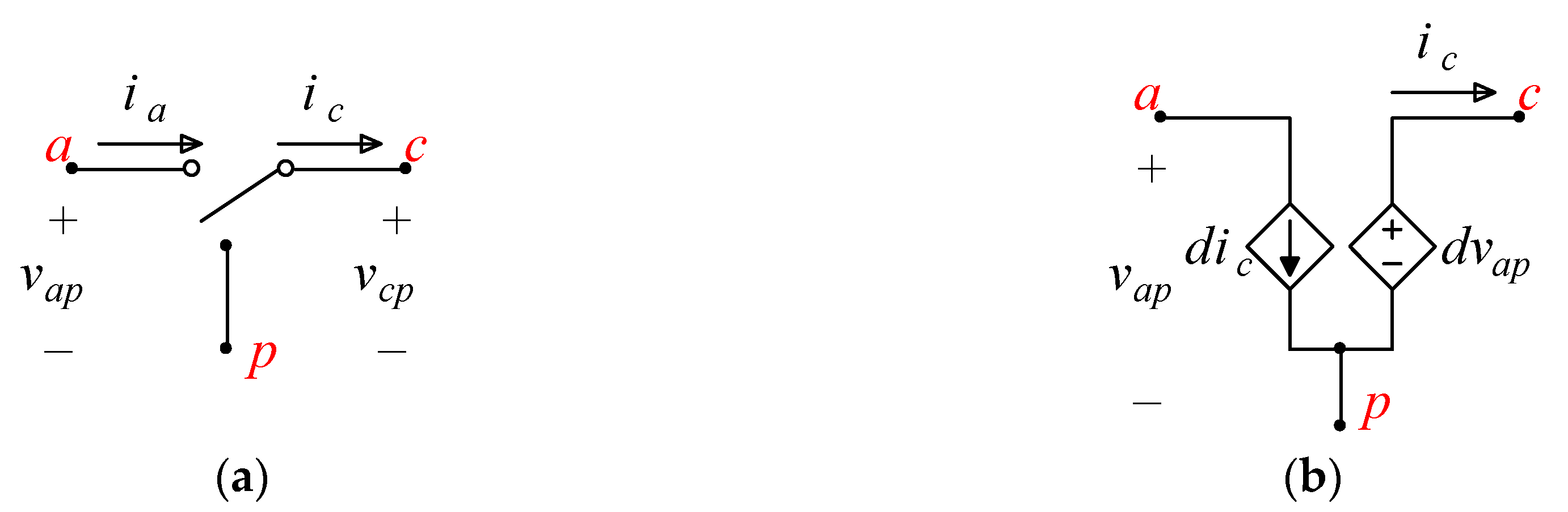
12] establishes an equivalent circuit model for a DC/DC converter by treating the basic switching units of the converter—power-switching transistors and diodes—as a three-terminal switching network and by averaging the voltages and currents at the terminals. A three-terminal switch can be represented by a single-pole double-throw switch, as shown in
Figure 1a (a-p and c-p are defined as voltage and current ports, respectively), which can be treated as a two-port network.
In the continuous conduction mode (CCM), the average terminal current and the average port voltage within a switching cycle
T are
ia =
dic and
vcp =
dvap, respectively, where
d represents the duty cycle. Thus, the large-signal circuit-averaged model of a three-terminal PWM switch is composed of two controlled sources, as shown in
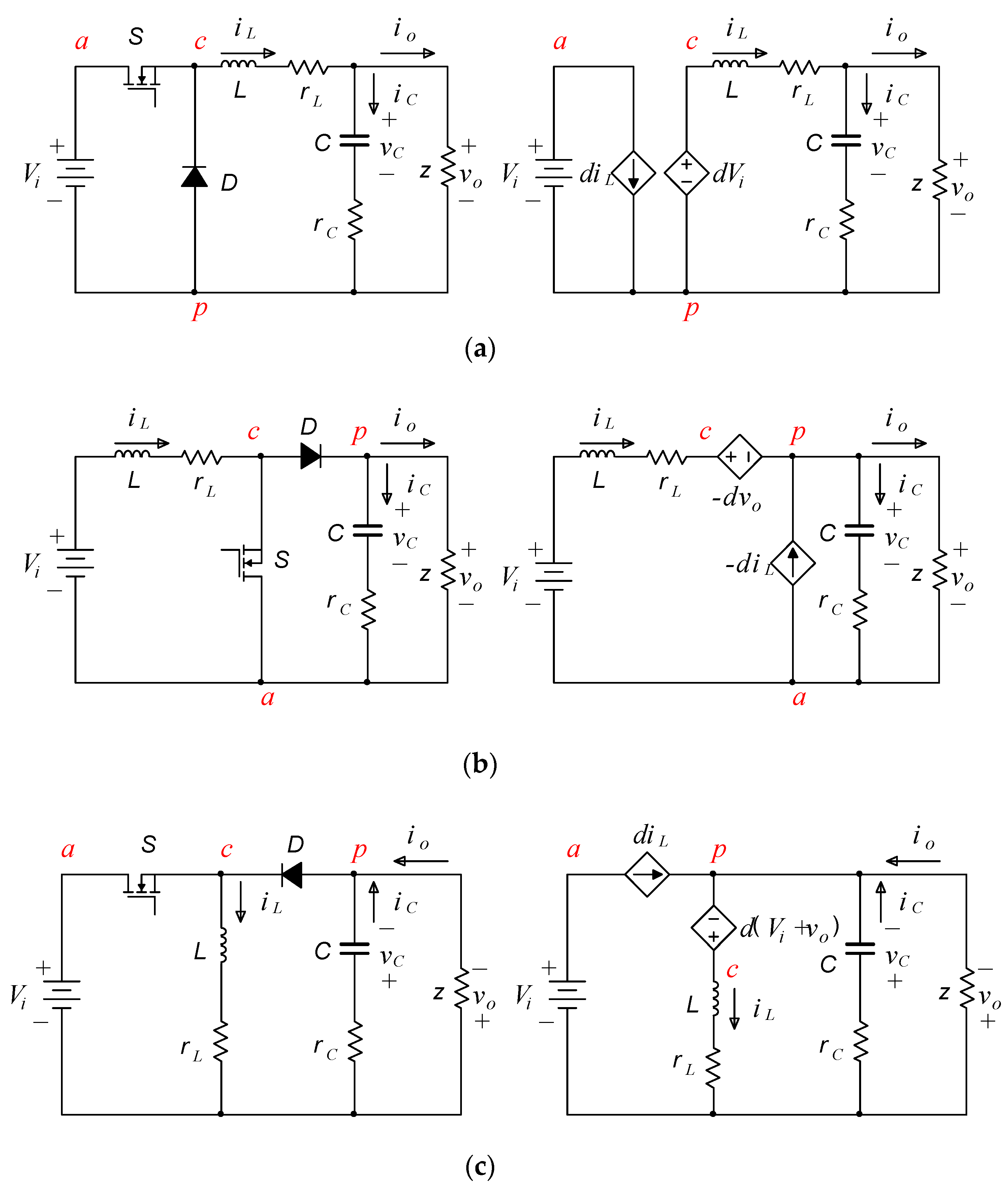
Figure 1b. The large-signal averaged models of a buck converter, a boost converter, and a buck–boost converter are established using this method, as shown in
Figure 2.
The equations for the main circuit of the above converters are listed in
Table 1. Here,
Vi represents the input DC voltage;
vo represents the output voltage;
iL represents the inductive current;
iC represents the capacitive current;
io represents the output current;
Z represents the load impedance, for a resistive load,
Z(
s) =
R; and
rL and
rC represent the equivalent series resistance (ESR) of the inductor and capacitor, respectively. The voltage and current variables in the above equations are average values. Note that the load impedance
Z does not appear in the equations; thus, these models are applicable to any load type, including nonlinear load. Based on
Table 1, block diagrams of the large-signal averaged models of the three converters can be produced, as shown within the black dotted boxes (excluding the transfer function of the PWM modulator, 1/
VM) in
Figure 3.
3. Feedback Linearization Based on the Inverse System Method
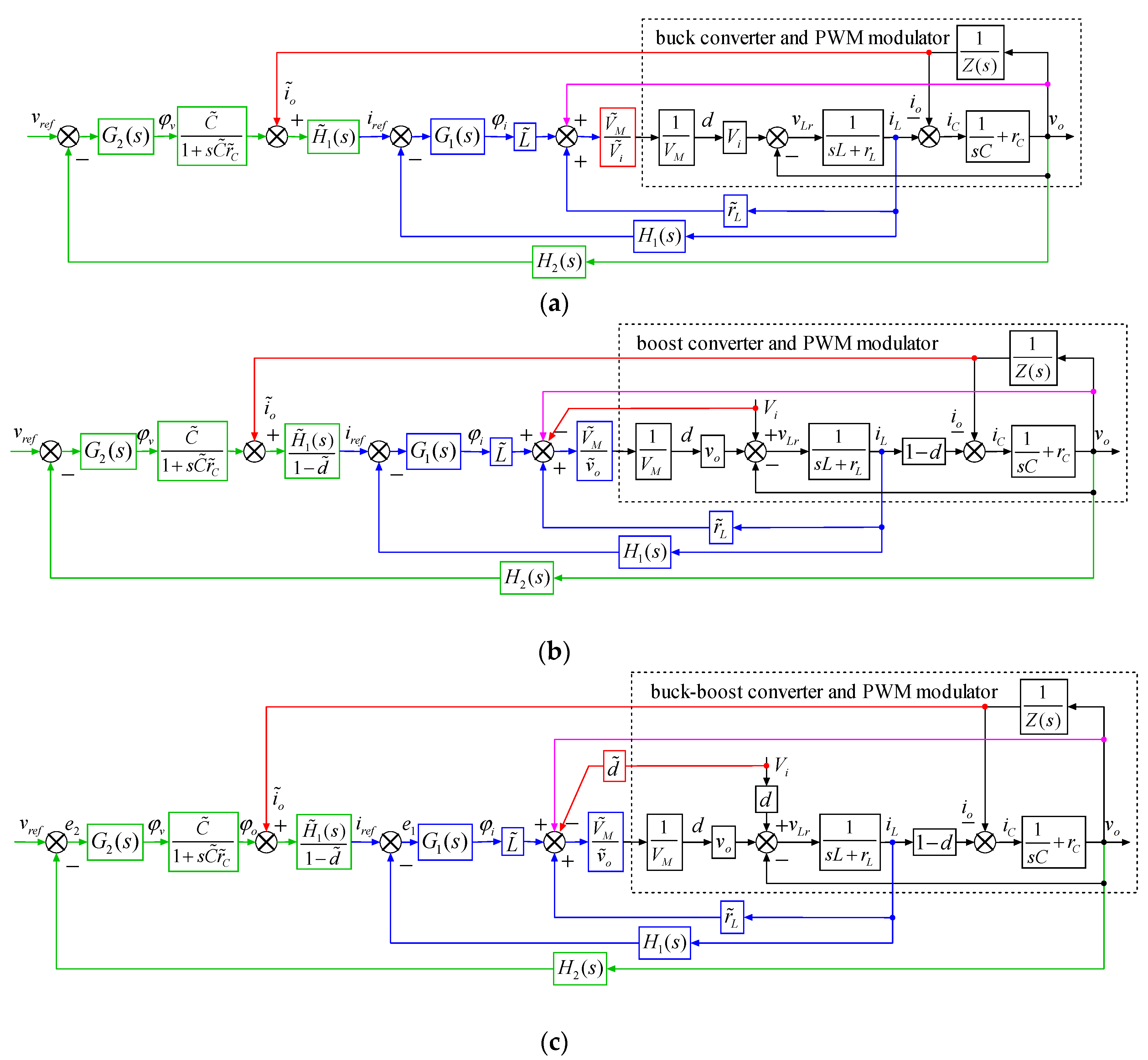
A voltage and current double closed-loop control system is selected for each of three types of converter (buck, boost, and buck–boost).
Figure 3a–c show the block diagrams of the control systems. Within the black dotted box in each of
Figure 3a–c is the controlled objects, including the main circuit of the converter and a PWM modulator.
G1(
s) and
G2(
s) are the current-loop and voltage-loop linear feedback controllers, respectively.
H1(
s) and
H2(
s) are the current-loop and voltage-loop feedback elements, respectively. The feedback current and voltage are directly proportional to the current and voltage in the designed path, therefore,
H1(
s) =
h1,
H2(
s) =
h2, where
h1 and
h2 are constant. Variables marked with “~” are estimation or measure variables. Each control system is decomposed into four sub-modules, namely, a disturbance input decoupling sub-module (red), a decoupling state feedback sub-module (purple), a current-loop sub-module (blue) and a voltage-loop sub-module (green). Disturbance input decoupling is achieved to offset the impact of the disturbances of power supply and load. Decoupling state feedback is employed to eliminate cross-coupling of the controlled loops and independently control these loops. An inverse-system decoupler and a linear feedback controller are designed for the voltage-loop and current-loop controlled objects, respectively, with the aim to compensate these two objects to two pseudo-linear systems. The following section focuses on finding a solution for the inverse-system decoupler.
3.1. Definition of an α-Order Integral Inverse System
“Inverse” is a concept of universal significance. The relationship between a dynamic system and its inverse system can be viewed as a relationship between mapping and inverse mapping. A system that can form an identity mapping relationship with the original system is referred to as the unit inverse system of the original system. However, generally, this structure includes a pure differentiation element. It is an unphysical structure that cannot be implemented in engineering practice. Therefore, there is a need to introduce a control structure that can be implemented, i.e., an
α-order integral inverse system, which is defined as follows [
31]:
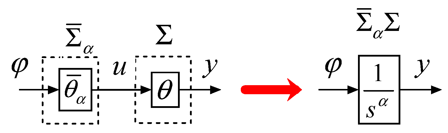
For a given system, Σ, its input vector, output vector, and state variable are denoted by u(t) Rr, y(t) Rm and x(t) Rn, respectively, and the initial condition is set as x(t0) = x0. The mapping relationship of Σ is described with an operator, θ, as y = θu. If an r-dimensional input m-dimensional output system with a mapping relationship of
(ϕ is the α-order derivative of y, i.e., ϕ (t) = y(α)(t)), , exists, when the initial state of is the same as that of Σ, if operator meets the following condition: , then is referred to as the α-order integral inverse system of Σ.
System
expressed with composition operator
is equivalent to an
α-order integrator series system, as shown in
Figure 4. It is a pseudo-linear system, thus various linear control theories can be employed to complete the design of the closed-loop control system.
3.2. Inverse System of the Current-Loop Controlled Object
The current-loop controlled object model is written in the form of a state-space equation:
where
iL represents the state variable. With
vLr as the control variable and
y =
iL as the output variable, based on the inverse-system solution method, the derivative of the output equation is continuously sought until
y(α) explicitly contains
vLr:
The relative-order of the system is
α = 1. Therefore, the system is first-order reversible. Let
ϕi =
y(1) be the new input. The first-order integral inverse system of Equation (1) is, thus, obtained as follows:
Thus, this inverse-system decoupler and the original system form a pseudo-linear system. Take
Figure 3c as an example, whose output is as follows:
If the measure quantities agree closely with the true values, the open-loop transfer function of the current loop is
The decoupled current-loop controlled object is equivalent to a first-order integral linear system,
y =
s−1ϕi. If a current-loop controller is designed to allow
iL to be satisfactorily capable of tracking the changes in
iref, then
IL(
s)/
Iref(
s) ≈ 1/
H1(
s).
3.3. Inverse System of the Voltage-Loop Controlled Object
The voltage-loop controlled object model is:
where
iC represents the state variable. With
iC as the control variable and
vo as the output variable, the transfer function corresponding to Equation (6) obtained by Laplace transformation is
Let
(
s) =
sVo(
s) and
IC(
s) be the new input and output variables, respectively. The first-order integral inverse-system transfer function of Equation (7) is thus obtained:
This inverse-system decoupler is connected to the original system in series to form a pseudo-linear system. For example, the expression of the
Vo(
s) of
Figure 3c is
The open-loop transfer function of the voltage loop is obtained:
Therefore, the control problem is converted to a problem of controlling a pseudo-linear system that has a standard form.
4. Controller Design
After decoupling, the open-loop transfer functions of the current and voltage loops are both 1/
s. While multiple theories and methods exist for linear system control, the controlled objects involved here are a type of simple, standard special system—a first-order pure integral system. Therefore, the design of proportional–integral–derivative (PID) controllers for first-order pure integral systems based on the optimal control theory [
34] is discussed here with a view to obtain simpler and more direct results.
Each of the decoupled current-loop and voltage-loop controlled objects represented by Equations (5) and (10), respectively, is equivalent to a first-order integral linear system, whose state-space and output equations are
where
x,
φ and
y represent the state, input and output variables, respectively. Manifestly, this system is completely controllable and observable, and an approximate optimal control for this system exists. It is assumed that the desired system output is
r. A deviation of
e(
t) =
r −
y(
t) is introduced to convert the output regulator problem to an equivalent state regulator problem. The state-space equation in Equations (11) is then transformed to
The optimization objective is to find a function
φ*(
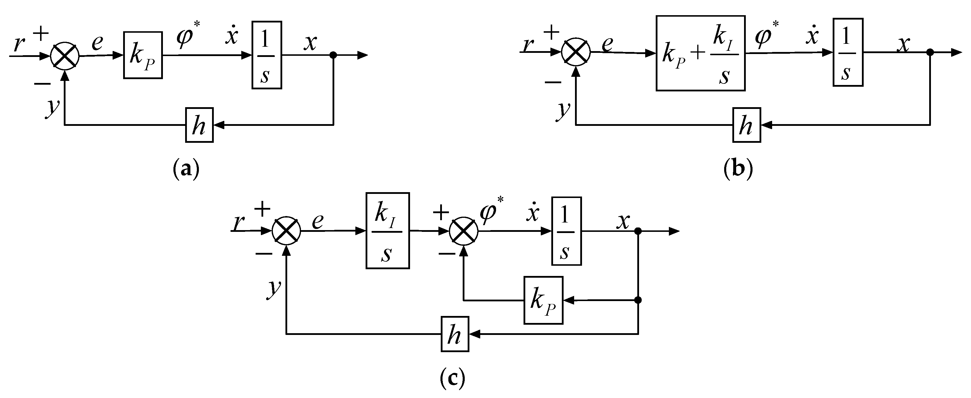
t) that minimizes the performance index under the constraint of the system equation. The linear quadratic regulator (LQR) and the integrated time absolute error (ITAE) optimization method can be used to design controllers. Three types of optimal controllers, P, PI, and I-P regulator are discussed here. If a P regulator is selected as the controller, then the closed-loop system is a first-order inertial system. If a PI regulator is selected as the controller, then the closed-loop system is a second-order system with a zero. When an I-P regulator is selected as the controller, the closed-loop system is a second-order system with no zero.
Figure 5 shows the structural diagrams of the optimal control systems, in which
ϕ* is the optimal control.
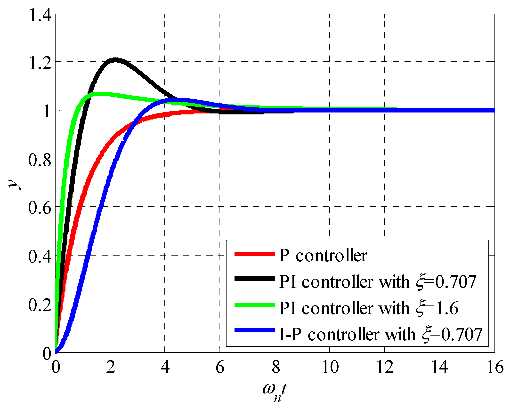
Table 2 shows the steady-state and dynamic performance indices of the aforementioned optimal control system. The natural frequency
ωn characterizes the transient response speed of the system. Of the frequency domain indices, the corresponding parameter is the bandwidth frequency,
ωb. After determining the
ωn or
ωb of the closed-loop system based on the settling time
ts requirements, the suitable controller coefficients,
kP and
kI can be determined to minimize the LQR or ITAE index of the system. Thereby ensuring that the system is optimal under the functional meaning of the performance indices and that the step response of the closed-loop system is in the desired form.
Figure 6 shows the unit step response curve of the closed-loop system.
5. Validation through Simulation and Experimentation
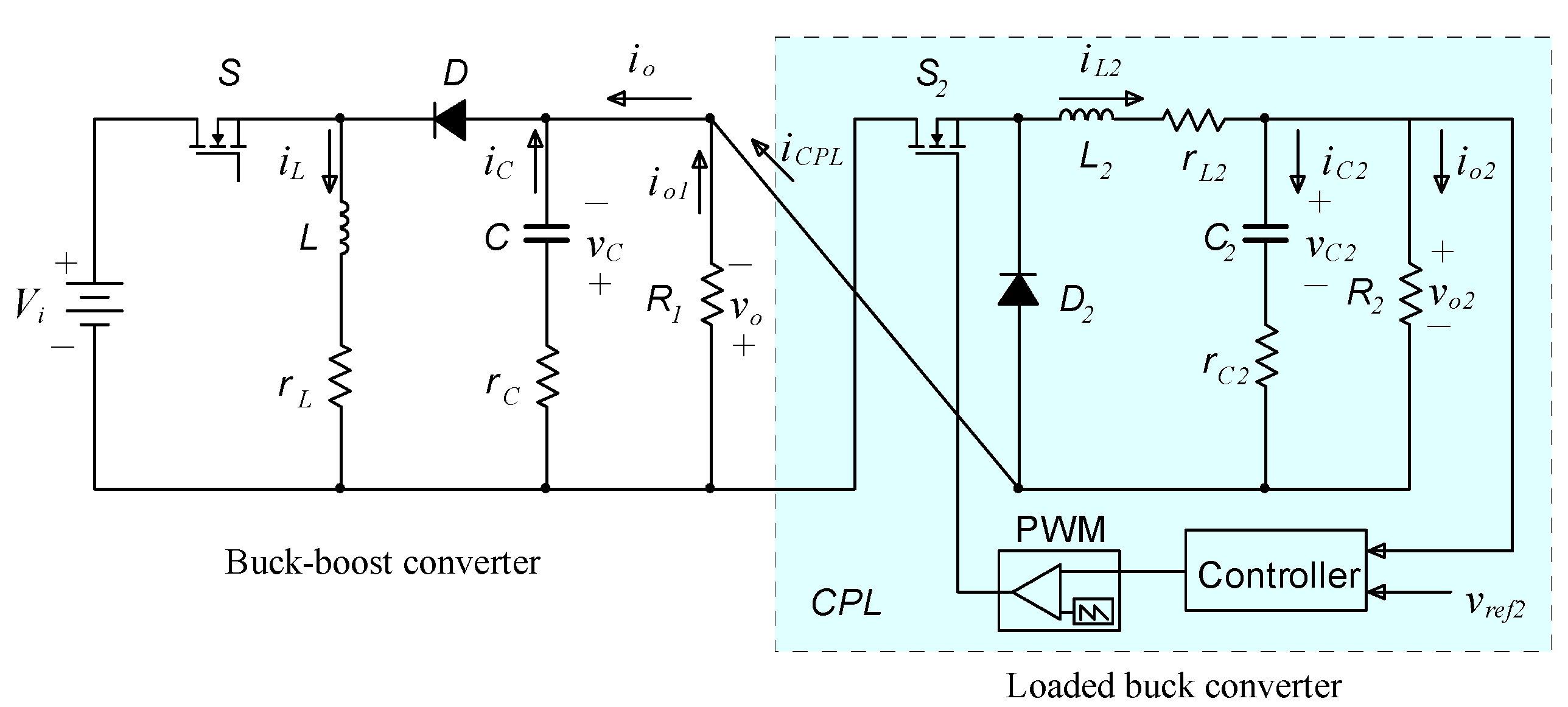
The proposed inverse-system decoupling control method was validated through simulation and experimentation based on buck–boost converters under resistive and CPL conditions.
The main circuit parameters of the designed buck–boost converter are as follows:
Vi: 20 V;
vo: 30 V; inductance,
L: 1 mH;
rL: 0.005 Ω; capacitance,
C: 470 μF;
rC: 0.005 Ω; and rated load resistance,
R1: 30 Ω. A closed-loop buck converter control system was connected to (and behind) the aforementioned buck–boost converter in cascades as a CPL, as shown in
Figure 7. The buck converter had a rated
Vi2 of 30 V, a rated
vo2 of 15 V, and a load resistance
R2 = 9 Ω.
For a buck–boost converter with a pure resistive load and a CPL connected in parallel, if the effects of
rL and
rC are not considered, then the control-to-output transfer function of its voltage loop is:
where
D′ = 1 −
D, 1/
REQ = 1/
R1 − 1/
RCPL,
RCPL =
Vo2/
P,
P =
Vo22/
R2. This is a NMP system. When
R2 > 7.5 Ω,
REQ > 0,
Gvc(
s) has a zero in the right half of the complex plane. When
R2 < 7.5 Ω,
REQ < 0,
Gvc(
s) has a pole in the right half of the complex plane, the system becomes an unstable NMP system. Therefore, a minute disturbance in the load can cause major changes in system properties.
When a PI controller
G2(s) =
kP +
kI/s is used, the characteristic equation of the closed-loop system is
where
a2 =
REQC −
h2DLkP/
D′,
a1 = 1
+ D +
h2D′
REQkP −
h2DLkI/
D′, and
a0 =
h2D′
REQkI. According to the Routh–Hurwitz stability criterion, the necessary and sufficient condition for stability of a second-order system is
a0 > 0,
a1 > 0, and
a2 > 0. Therefore,
a0 > 0 is necessary for system stability. To satisfy this condition, when
REQ > 0,
kI should satisfy
kI > 0; when
REQ < 0,
kI should satisfy
kI < 0. Obviously, these two conditions are contradictory. When the load on the system is subjected to a large disturbance, the original stable system may become unstable if a conventional linear controller is used.
For the inverse-system decoupling control system, a P controller was used in the outer voltage loop, and a PI controller was used in the inner current loop. The unit step response speed of the first- and second-order system is in direct proportion to ωb. In a double closed-loop system, the value of ωb of the inner loop should be far higher than that of the outer loop. Generally, ωb for the inner current loop is set to at least 5 to 10 times that of the outer voltage loop. The value of ωb of the inner current loop is constrained by and required to be far lower than the switching frequency. It is generally lower than 1/5–1/10 of the switching frequency. Here, the switching frequency of the converter is set to 50 kHz; the parameters of the PI controller for the inner current loop are set as follows: kP1 = 20,000 and kI1 = 20,000,000; the feedback factor (h1) of the inner current loop is set to 0.1; the parameters of the P controller for the outer voltage loop are set as follows: kP2 = 2000; and the feedback factor (h2) of the outer voltage loop is set to 0.1.
Simulations and experiments were performed under input voltage disturbance and load disturbance conditions. The results were compared with those of a conventional double closed-loop controller. For the conventional double closed-loop system, a PI controller was selected for the outer voltage loop,
G2(
s) =
kP2 +
kI2/s, where
kP2 = 1,
kI2 = 400, and
h2 = 0.1. The system phase margin was 55.3°, and the gain margin was 94 dB. A P controller was selected for the inner current loop,
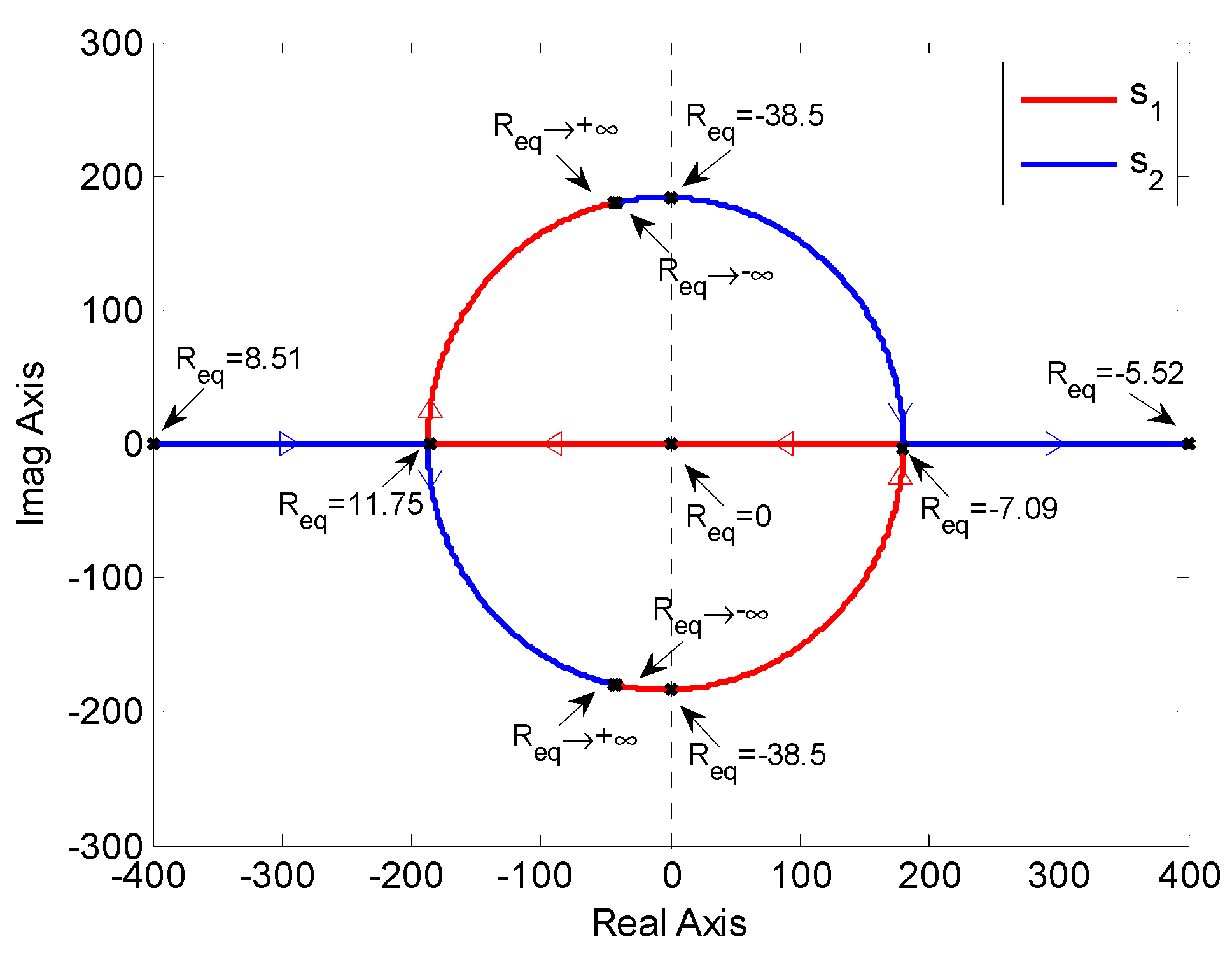
kP1 = 1. The root loci of Equation (14) are shown in
Figure 8, where
D = 0.6, and
REQ changes from -∞ to +∞. The roots are given by
When
REQ ≥ 0.32 Ω, both roots are on the left half plane and the system is stable. When
REQ < 0, a pair of complex conjugate roots cross the imaginary axis to the right half plane as |
REQ| decreases. A Hopf bifurcation occurs at
REQ = −38.5 Ω (i.e.,
P = 53.4 W and
R2 = 4.2 Ω) and the system loses its stability.
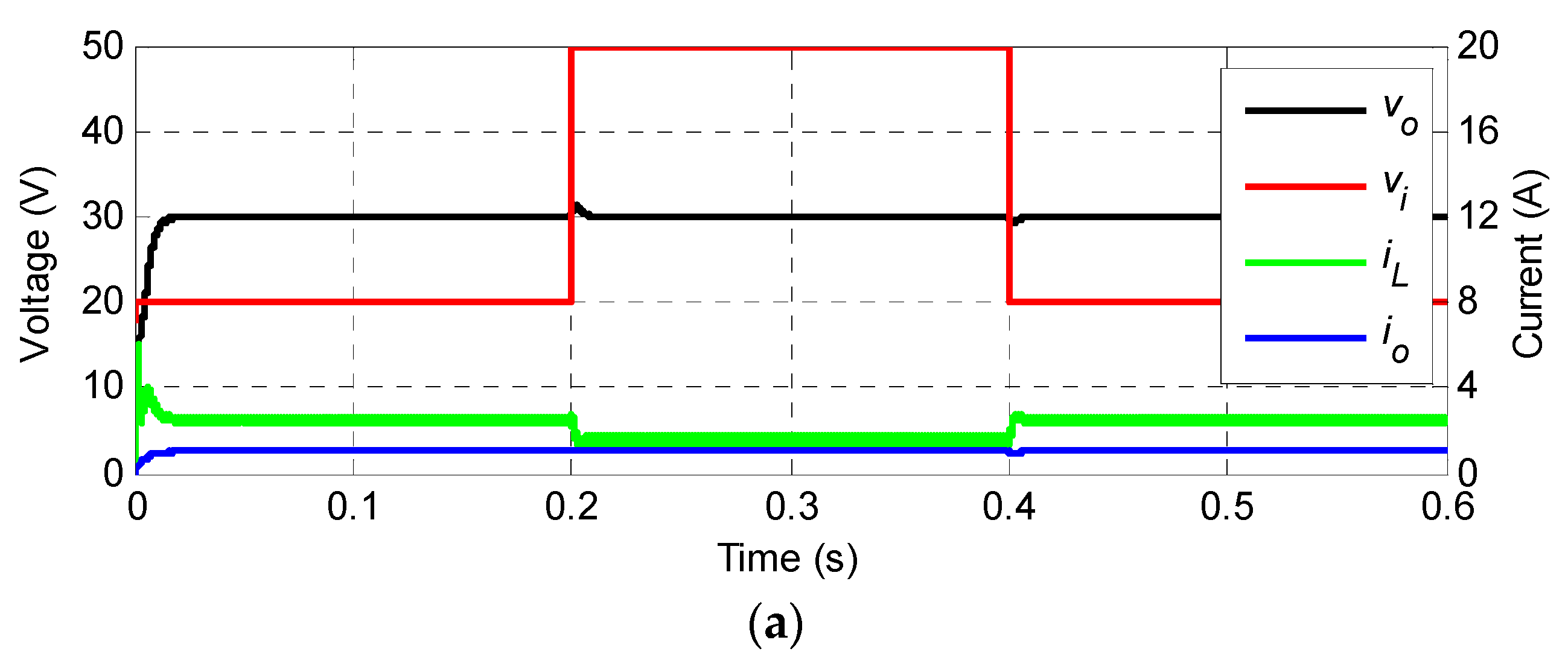
Figure 9 shows the simulated waveforms when the inverse-system decoupling control system and the conventional double closed-loop control system were used, respectively, under the rated operating conditions upon sudden changes in
Vi. The specific disturbance process is as follows:
Vi jumped from 20 to 50 V at 0.2 s and recovered to 20 V at 0.4 s. During the starting process, the inverse-system decoupling control system had a
vo overshoot, σ(
vo) of 0, and
ts = ca. 15 ms. In comparison, the conventional double closed-loop control system had a σ(
vo) of approximately 46%, and a longer
ts = ca. 26 ms. In addition, it had a significant
vo undershoot, and
vo reached the target value after multiple oscillations. During a sudden increase (sudden decrease) in the input voltage, the maximum increase (decrease) in conventional controlled output voltage was 15 V, and the output voltage essentially returned to the reference value after 23 ms. In contrast, the inverse-system decoupling controlled output voltage was virtually immune to input voltage disturbances.
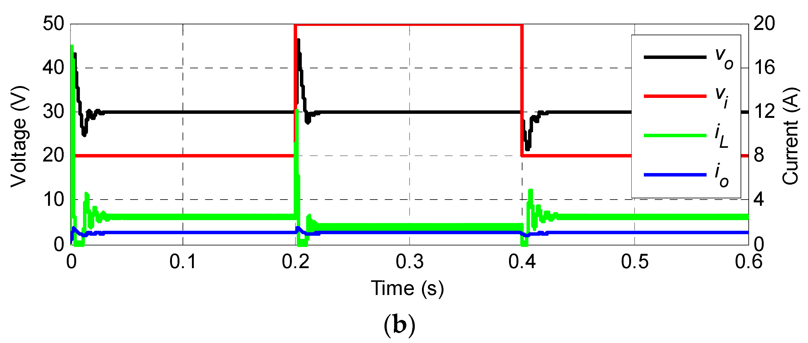
Figure 10 shows the simulated waveforms under the rated operating conditions upon sudden changes in
R2. When
R2 suddenly decreased (jumping from 9 Ω to 3 Ω, i.e., CPL power jumping from 25 W to 75 W) at 0.2 s, the maximum decrease in
vo resulting from the transition of the inverse-system decoupling control system was 4.36 V, and
vo rapidly recovered to the target value after 8 ms. In comparison,
vo sustained oscillation due to Hopf bifurcation and could not stabilize when the conventional double closed-loop control system was used. Therefore, the proposed controller performed significantly better than the conventional controller under input voltage and load disturbances. This is mainly reflected by small output voltage variations and shorter restoration times.
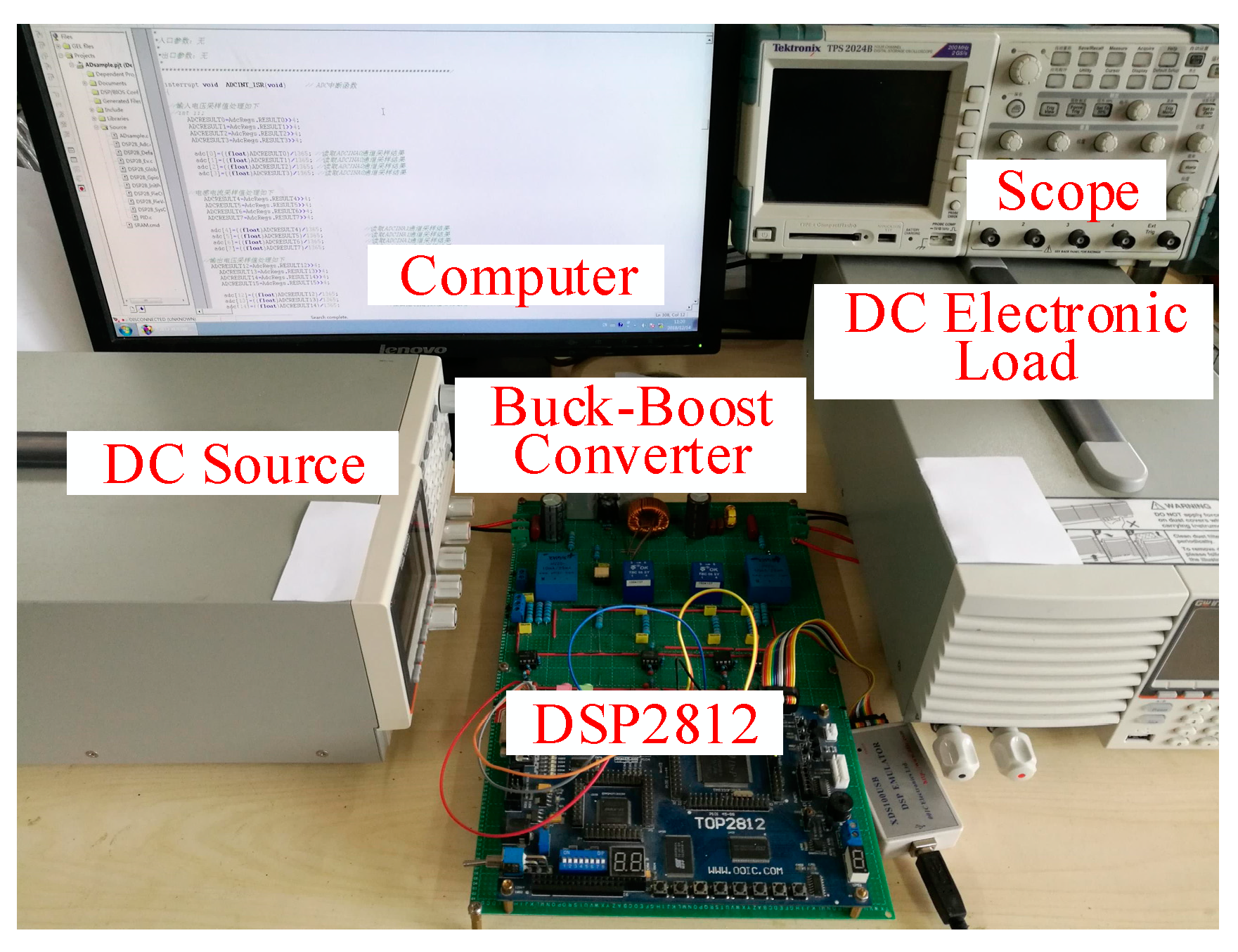
To further validate the control algorithm, a principle prototype of the buck–boost converter control system was fabricated in the laboratory. A GW Instek PEL-3031E programmable DC electronic load acted as the CPL.
Figure 11 shows the overall structure of the principle prototype. A TMS320F2812 digital signal processor chip was used as the controller. The large-signal inverse-system decoupling control algorithm was selected for the digital controller. The duty-cycle
d was evaluated as follows:
where
Tsam is the sampling period. The parameters of the main circuit and control system of the principle prototype were the same as those used in the simulations. The results were compared with those of a conventional double closed-loop controller.
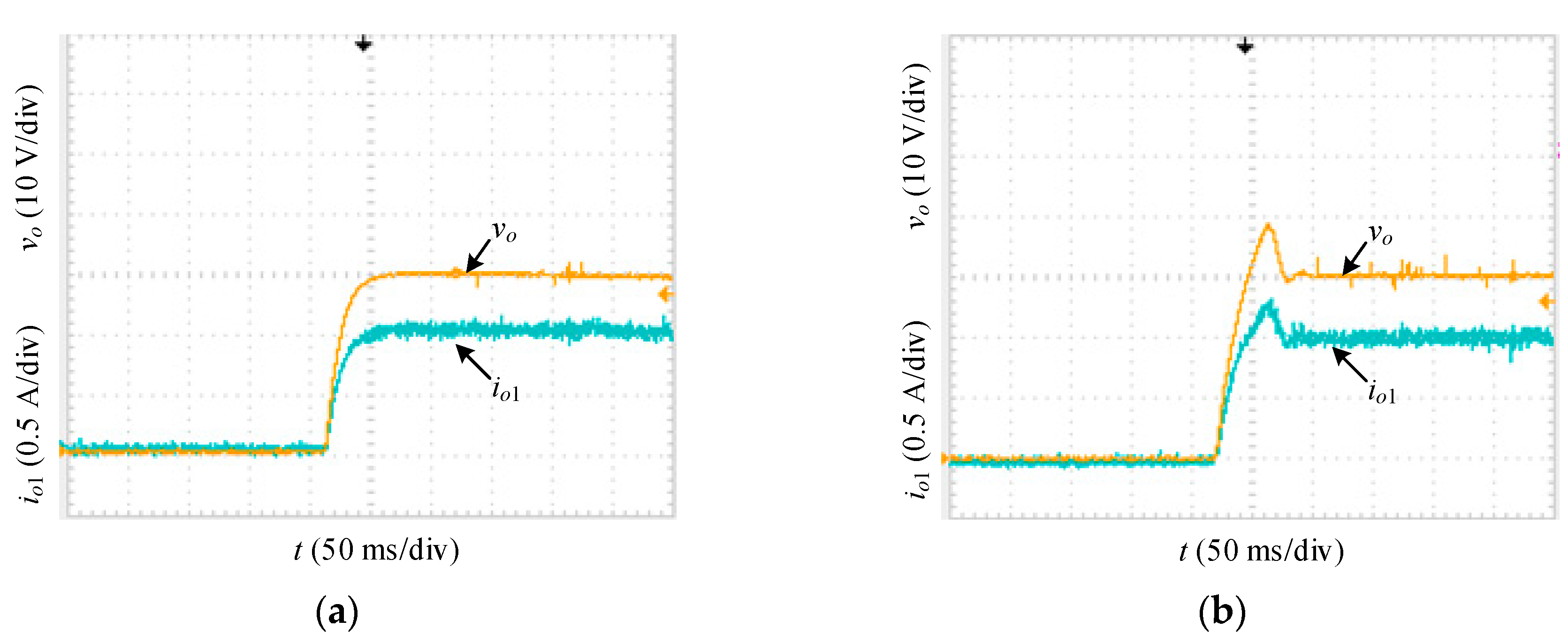
Figure 12 shows the step response waveform of the prototype system with a resistive load during the starting process. When a 20 V step signal was input, the
vo response curve of the inverse-system decoupling control system had no overshoot, In comparison, the conventional double closed-loop control system had a σ(
vo) of 33%. Experiments were conducted under jumping input voltage conditions.
Figure 13 shows the waveforms of
vo and
io when the input voltage
Vi jumped from 20 V to 50 V. The maximum increase in the inverse-system decoupling controlled output voltage
vo was 3 V, and
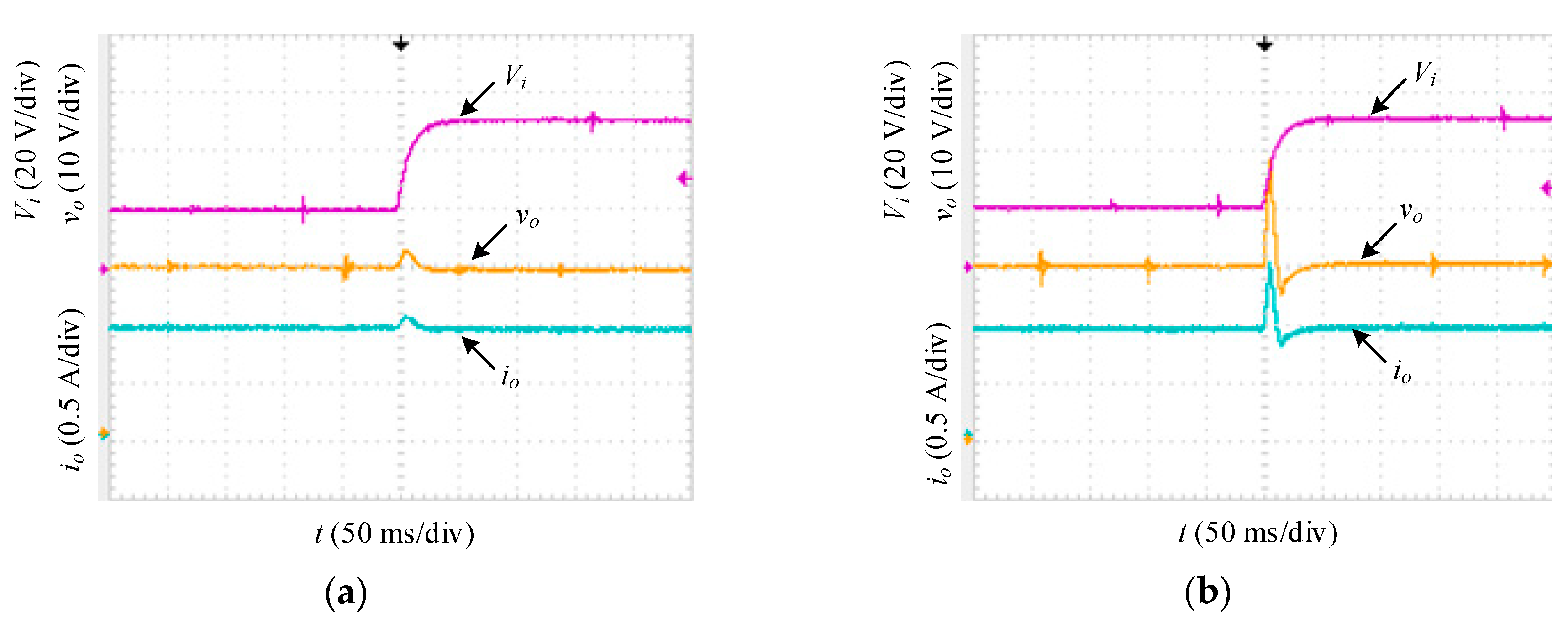
vo recovered to the target value after 12 ms. In contrast, the maximum increase in the conventional double closed-loop control system output voltage was 14 V, and the restoration time was 25 ms.
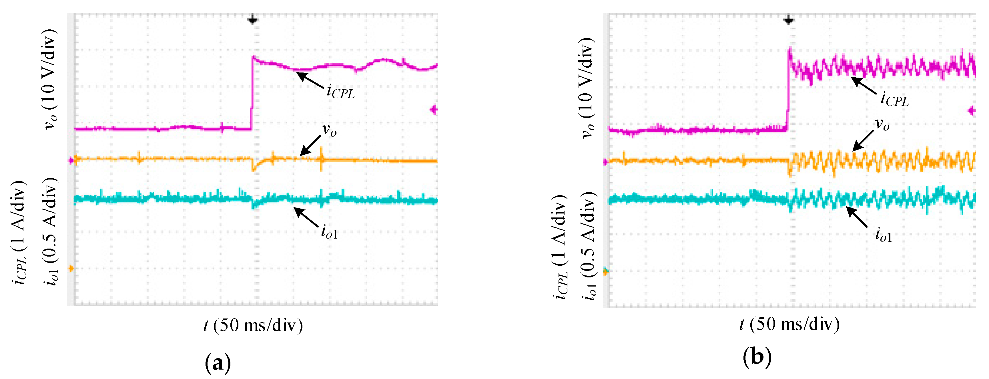
Figure 14 shows the step response waveforms of the prototype system with a pure resistive load and CPL connected in parallel. During startup, the CPL power was
P = 25 W, and the buck–boost converter equivalent impedance was
REQ = 180 Ω. The startup characteristics of the converter were similar to those of the system with a pure resistive load as shown in
Figure 12.
Figure 15 shows the waveforms of voltage and current when the CPL jumped from 25 W to 75 W with
REQ = −20 Ω. At the instant of the load jump, the inverse-system decoupling controller effectively controlled the converter, and
vo recovered to the target value within approximately 18 ms. In comparison, the conventional double closed-loop controller did not effectively control the converter. Under load disturbances,
vo underwent oscillations due to Hopf bifurcation. The experimental results match the root locus analysis and the simulation results. However, the Hopf bifurcation point is slightly different from that predicted by Equation (14). Because Equation (14) is deduced from a small signal model which ignore nonlinear terms and ESR of the converter.
Based on the experimental results, under the control of the inverse-system decoupling converter, the buck–boost converter exhibited excellent dynamic properties at the starting stage and excellent disturbance resistance. These observations were consistent with the simulation results and the theoretical analysis.


