
Metal–Organic Frameworks–Based Memristors: Materials, Devices, and Applications
Abstract
:1. Introduction
2. MOFs-Based Memristors
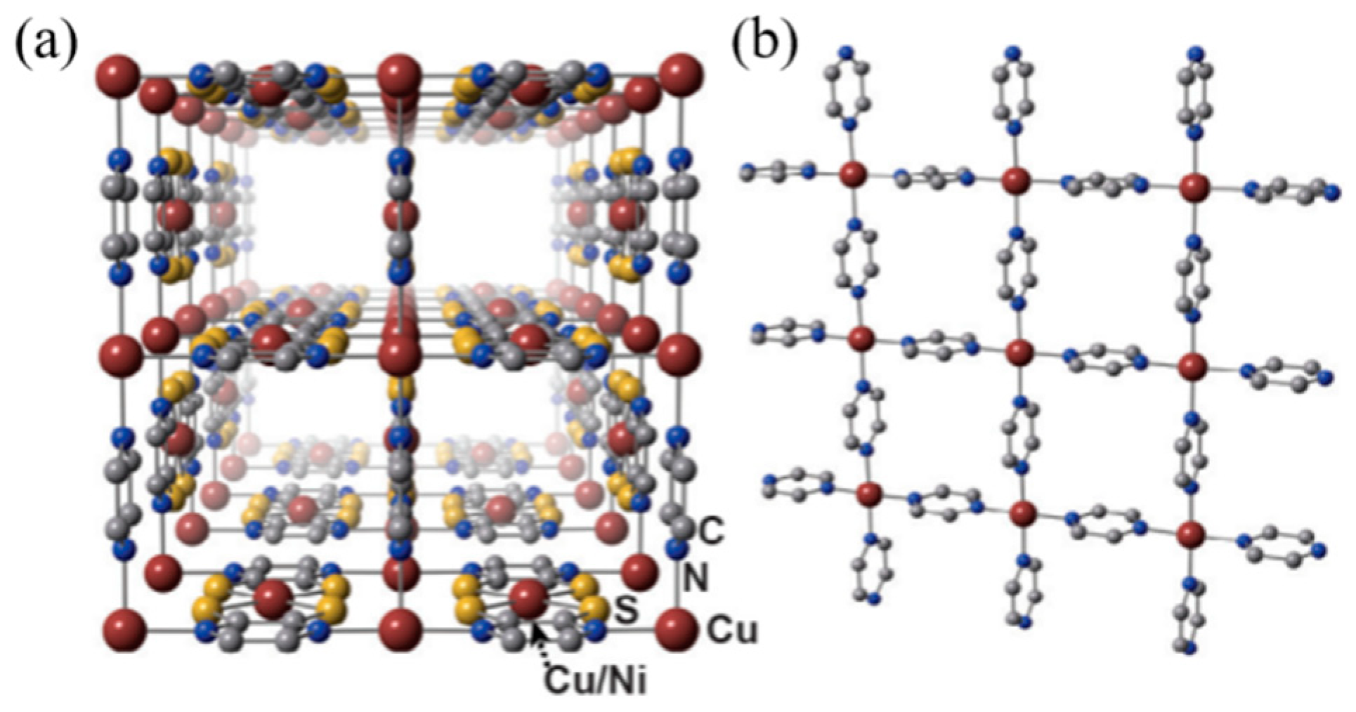
2.1. Materials Properties
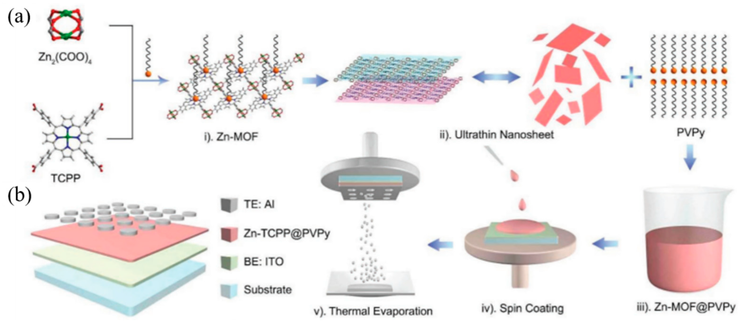
2.2. Synthesis of Functional MOFs
2.2.1. Solvothermal Reaction
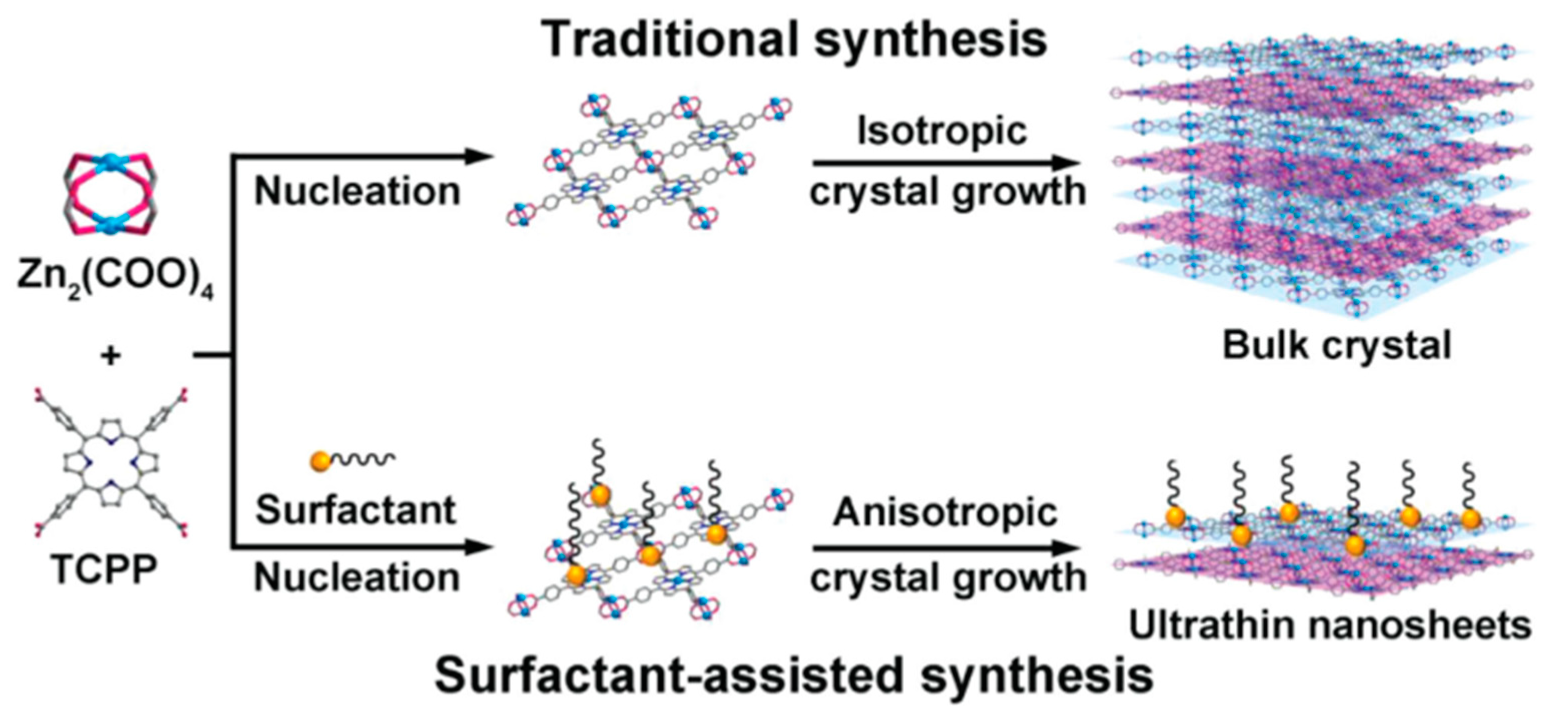
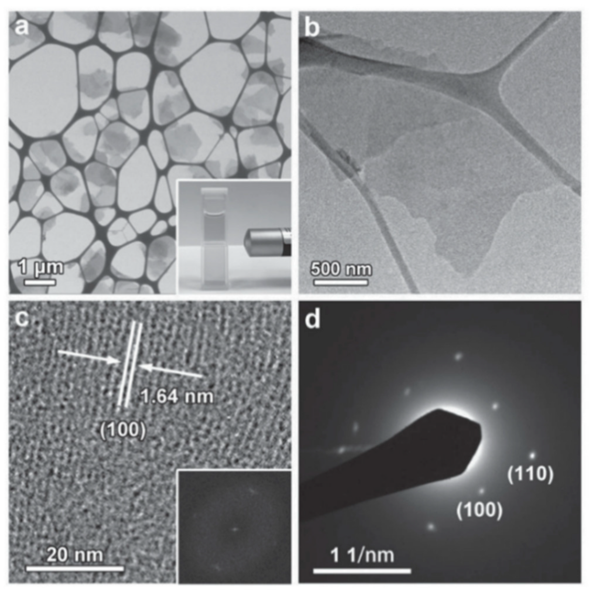
2.2.2. Surfactant-Assisted Method
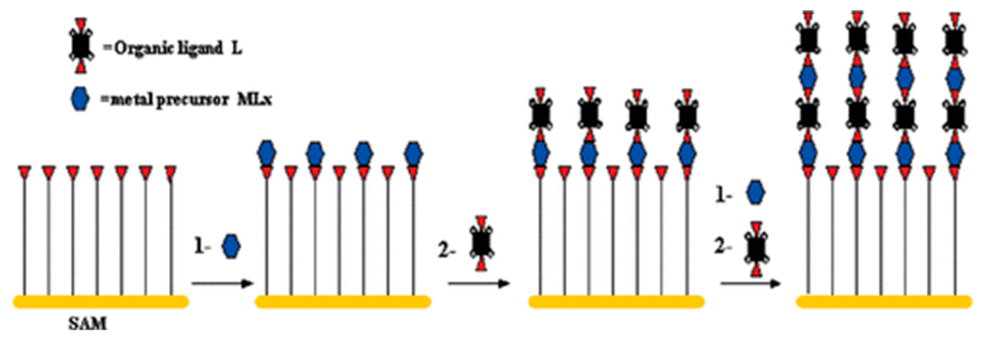
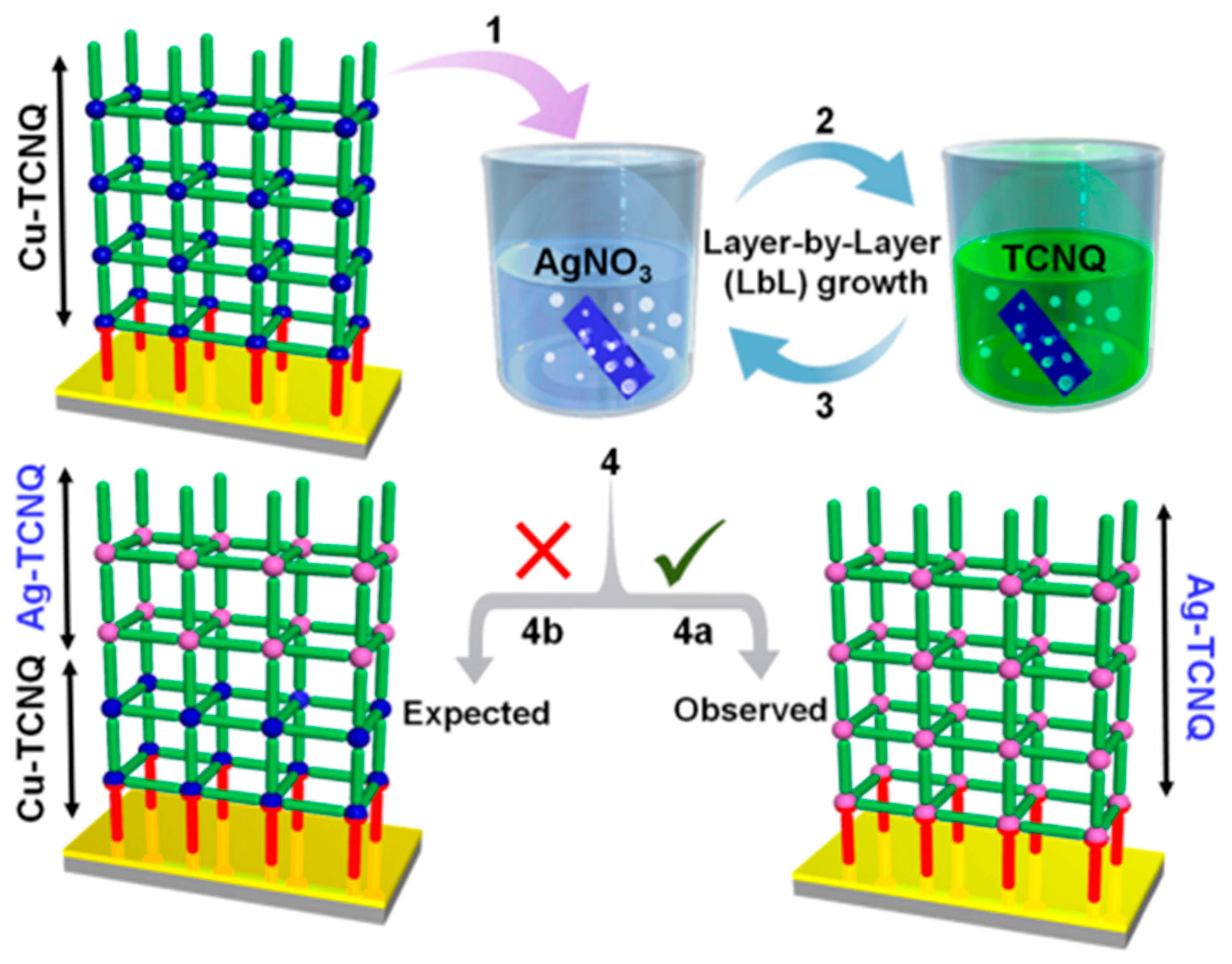
2.2.3. Liquid Phase Epitaxy Approach
2.2.4. Template Method
2.2.5. Microwave Heating
2.2.6. Interface Synthesis
2.2.7. Electrochemical Synthesis
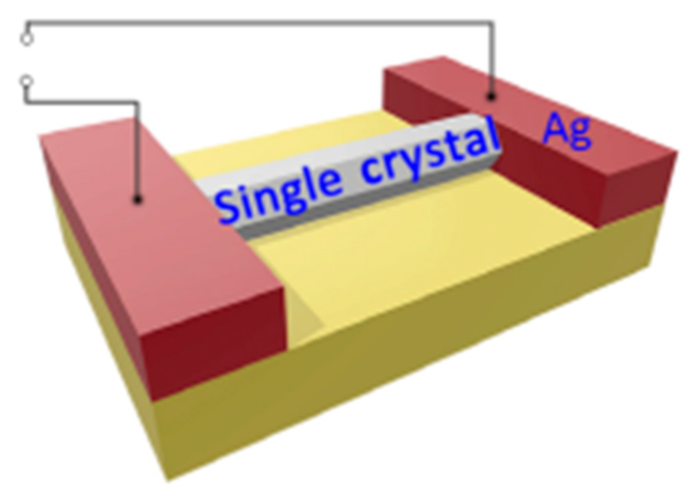
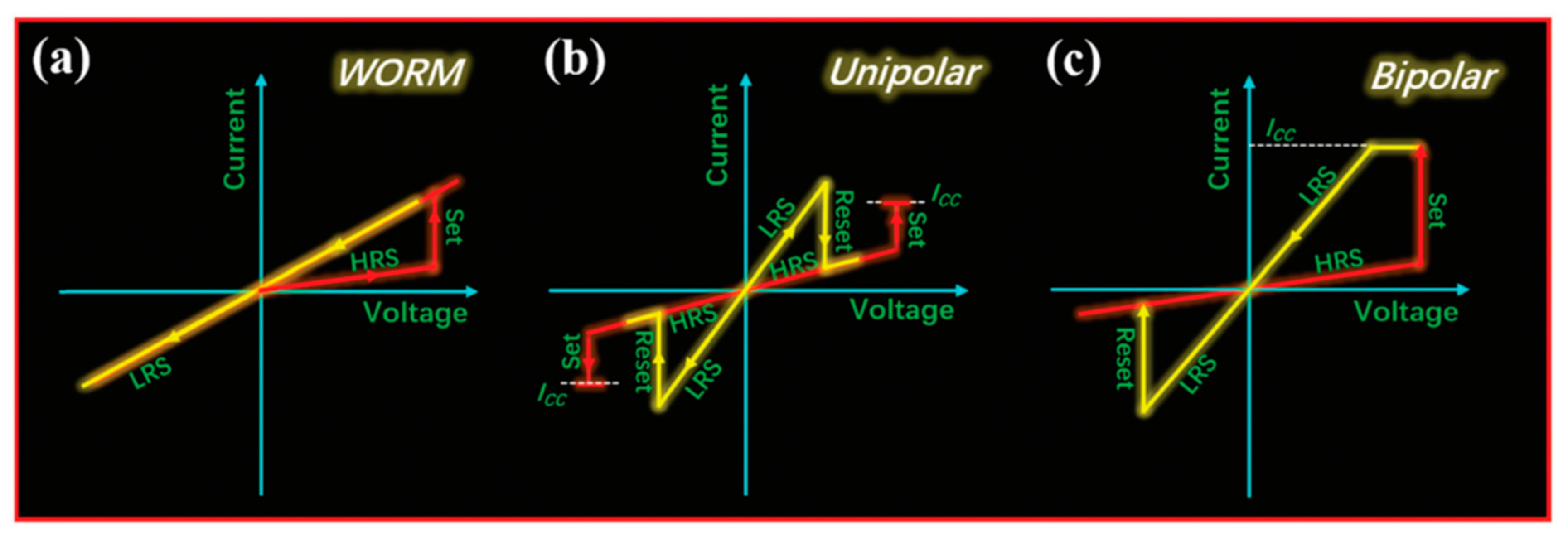
2.3. Device Structure and Electrical Parameters
3. Memristive Switching of Metal Organic Frameworks
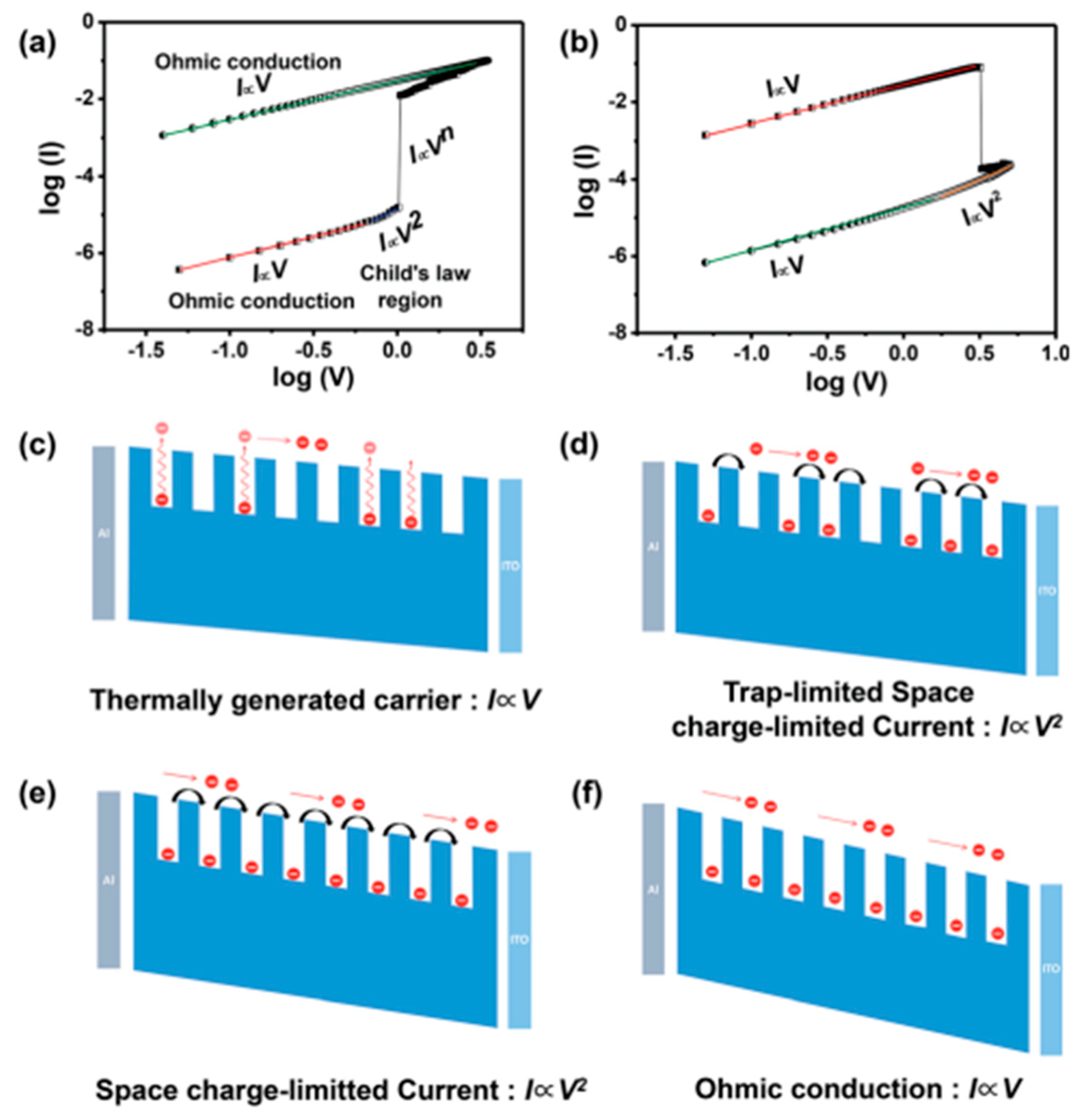
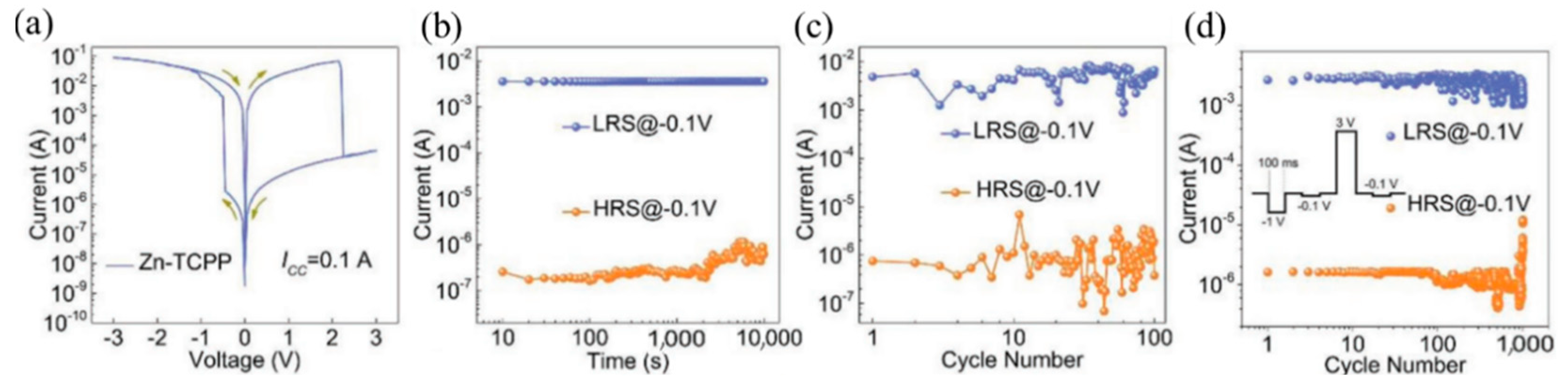
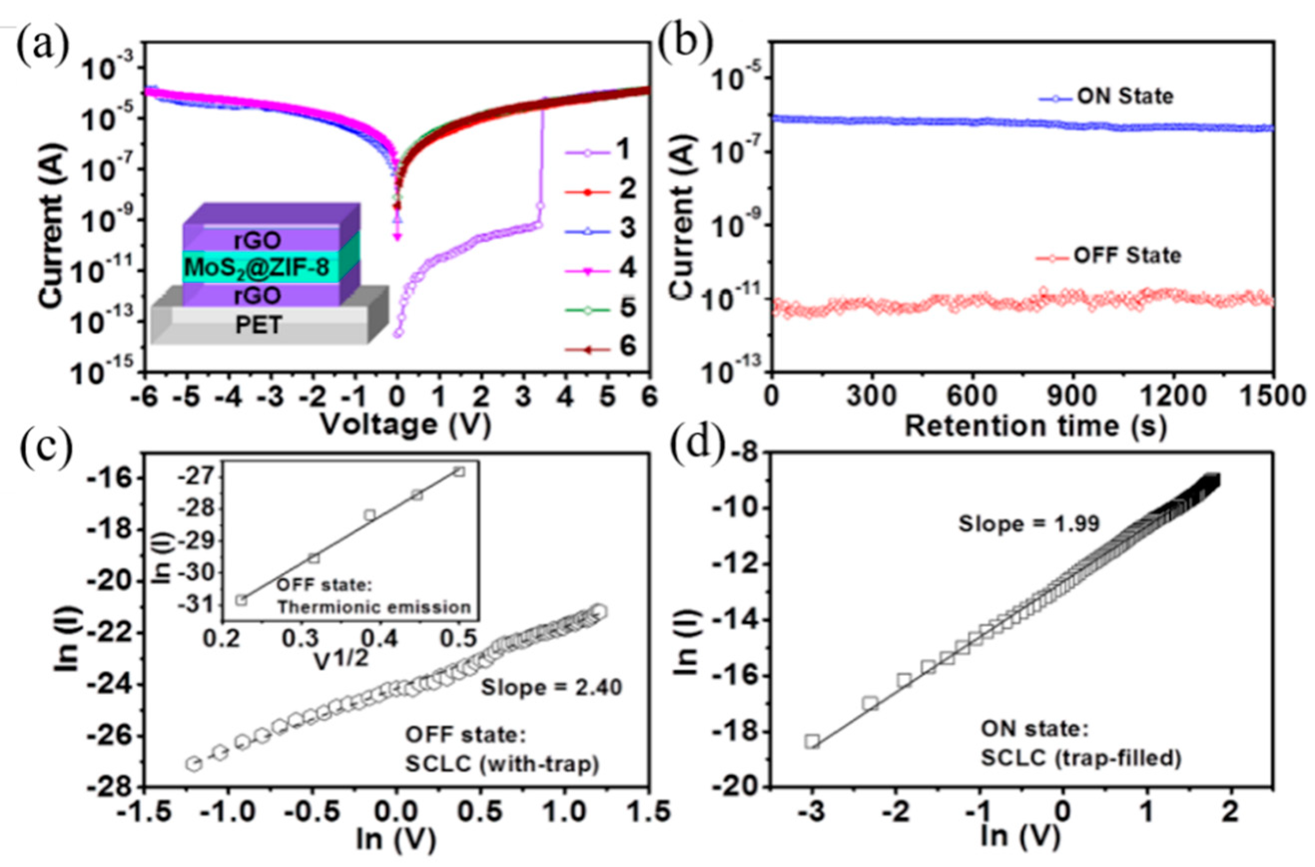
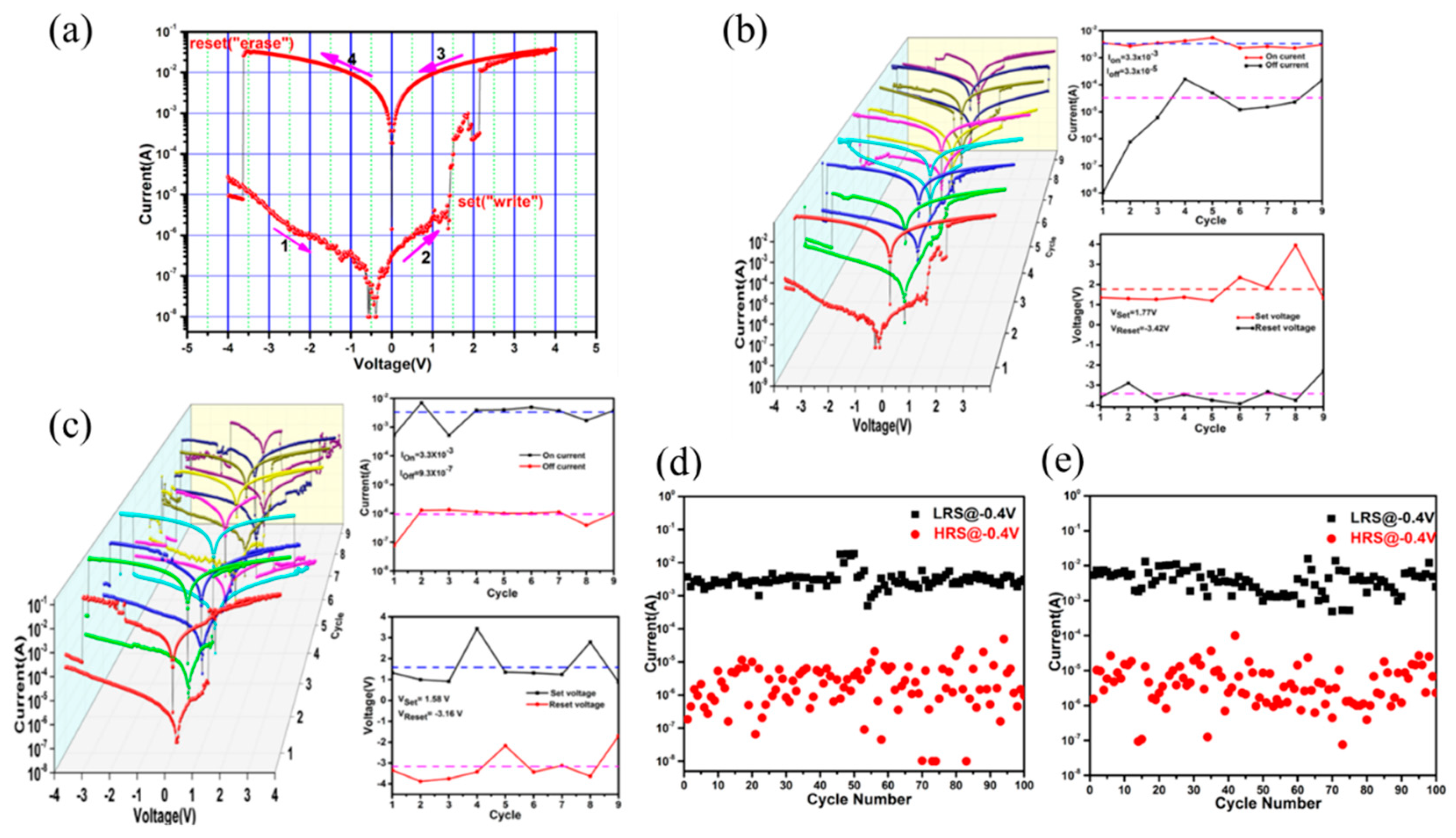
3.1. Charge Trapping
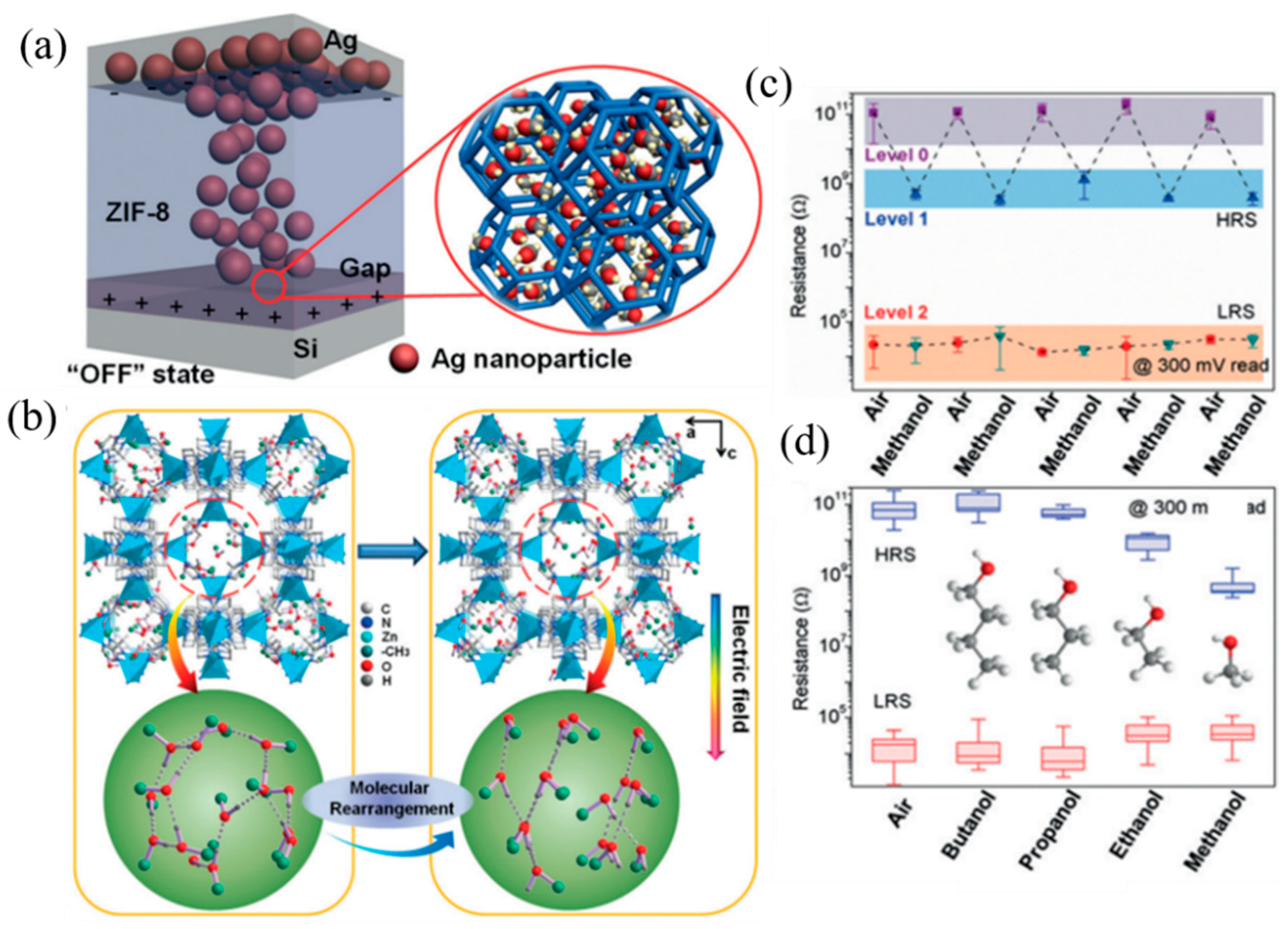
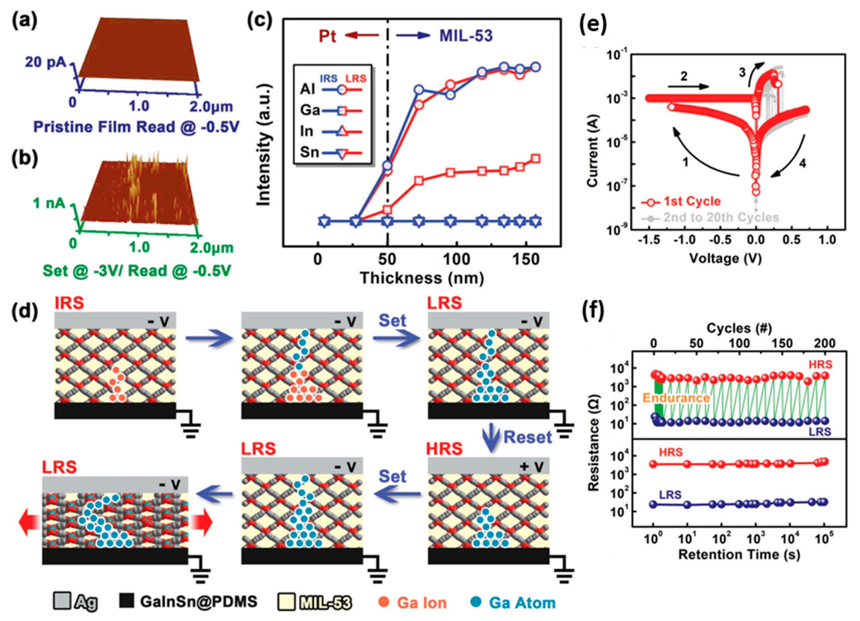
3.2. Ion Penetration
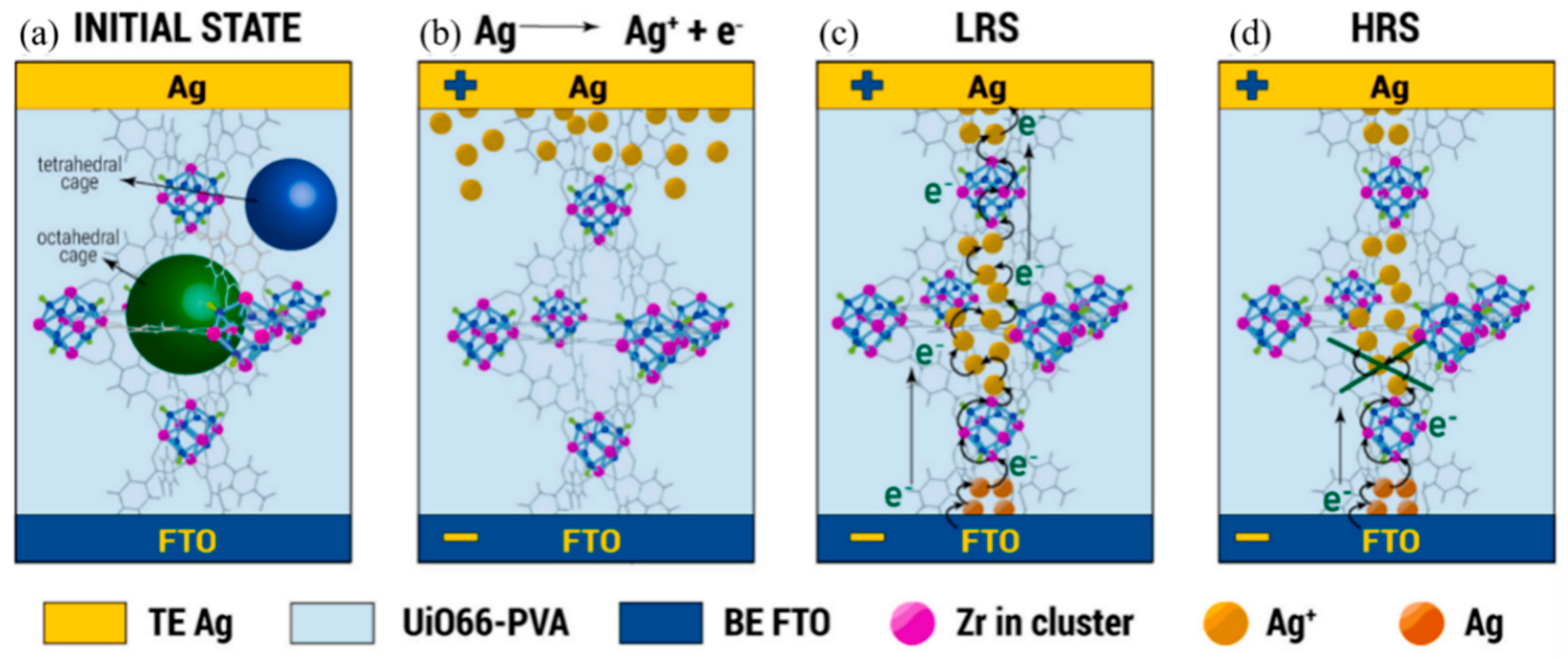
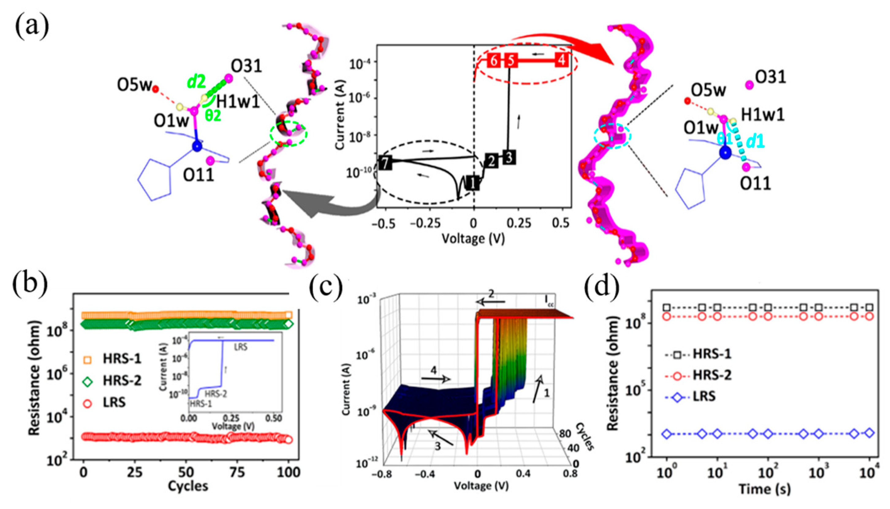
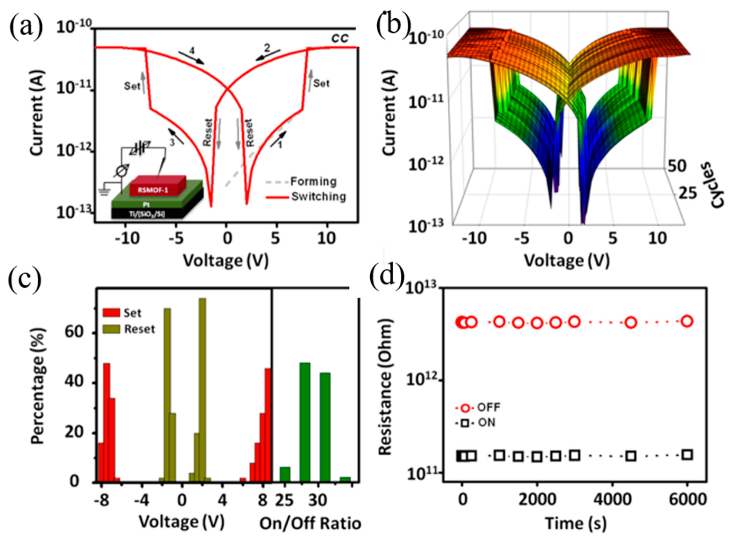
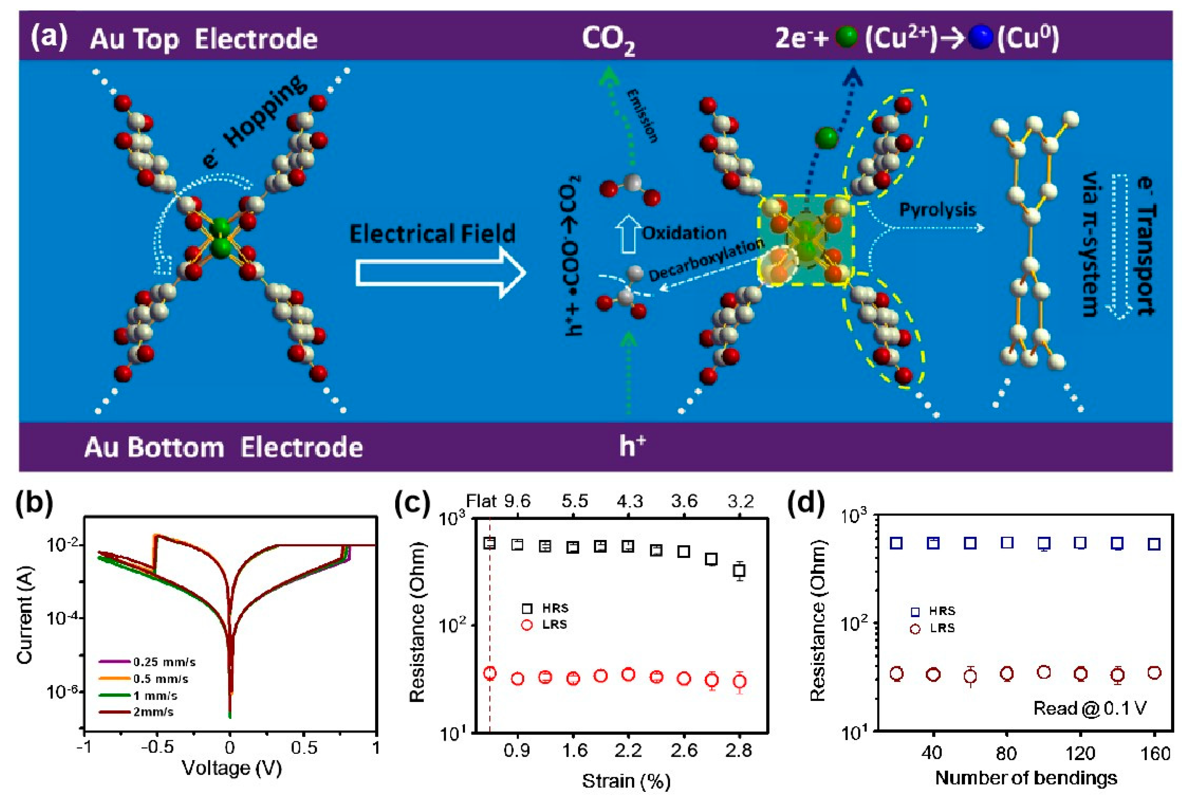
3.3. Skeleton Reorganization
3.4. Other Mechanisms
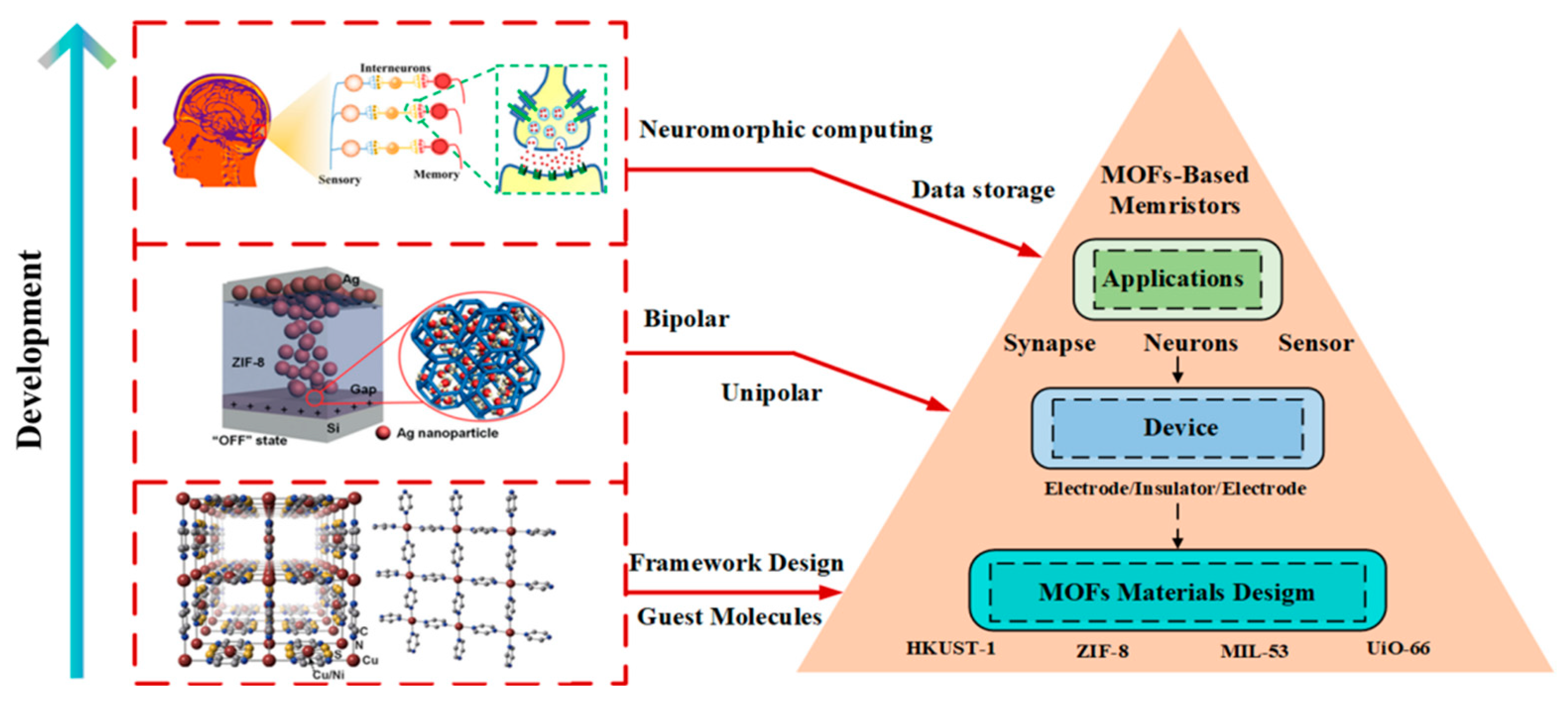
4. Application of MOFs-Based Memristor
4.1. Data Storages
4.2. Artificial Synaptics for Neuromorphic Computing
4.2.1. Electrical Artificial Synaptic
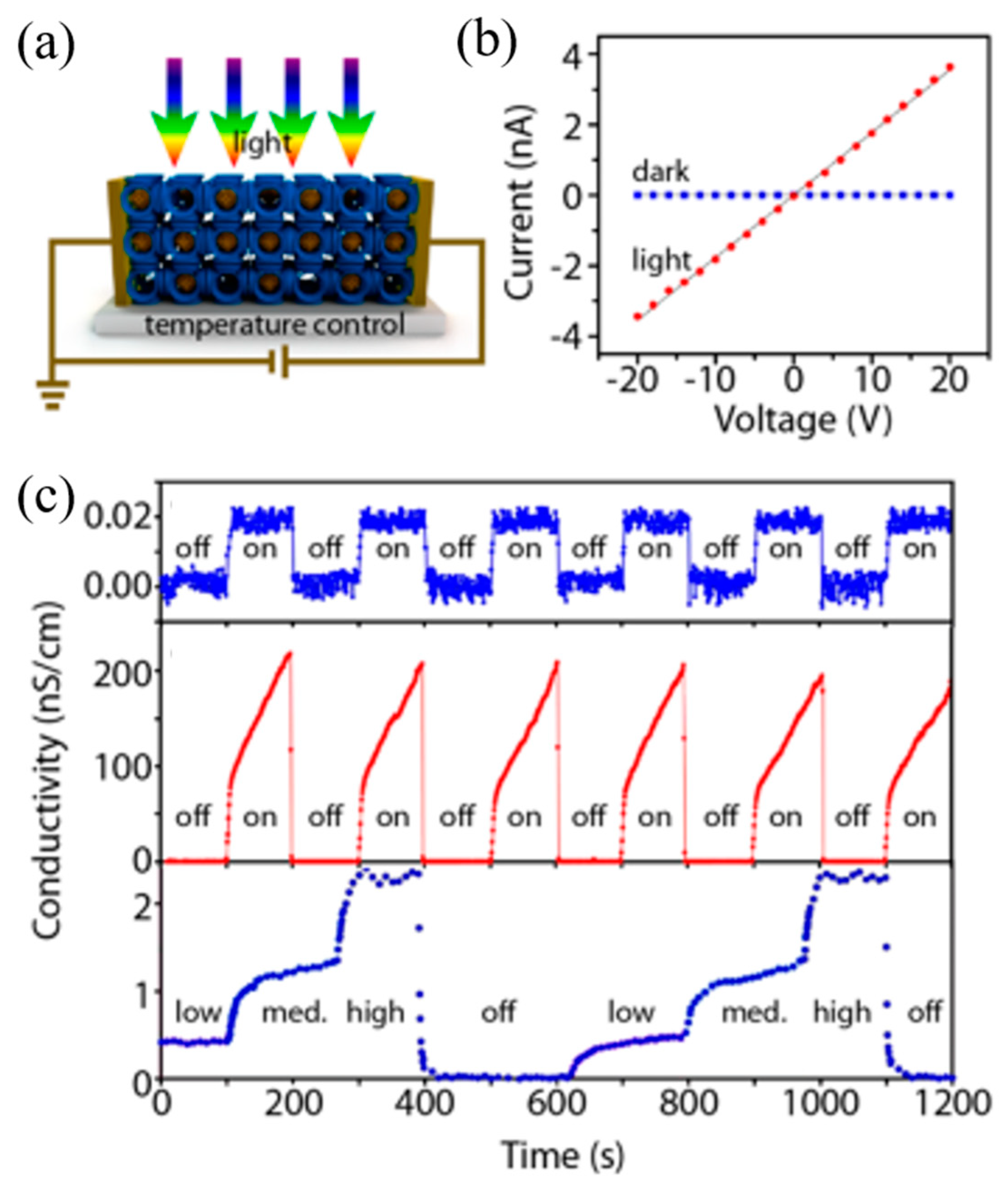
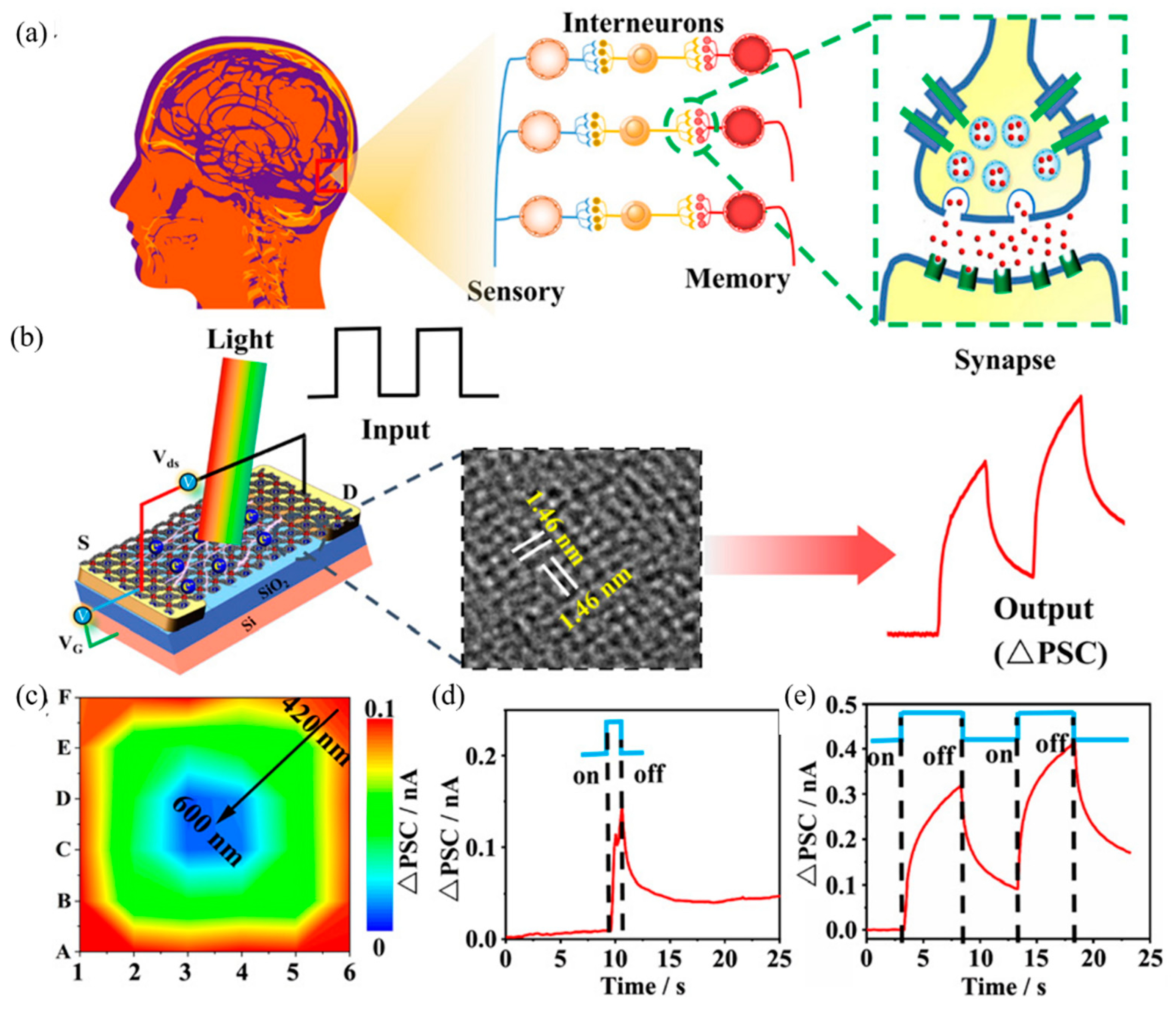
4.2.2. Optical Artificial Synaptic
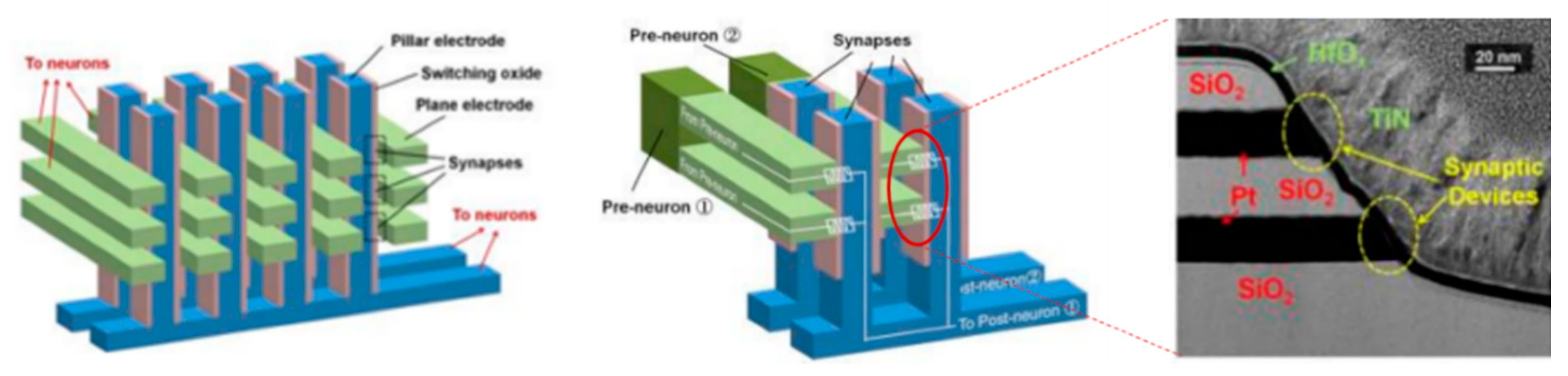
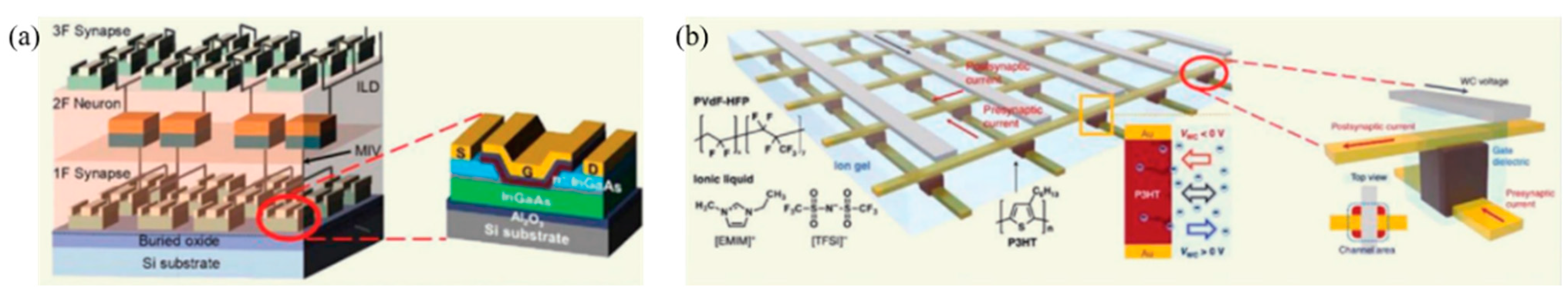
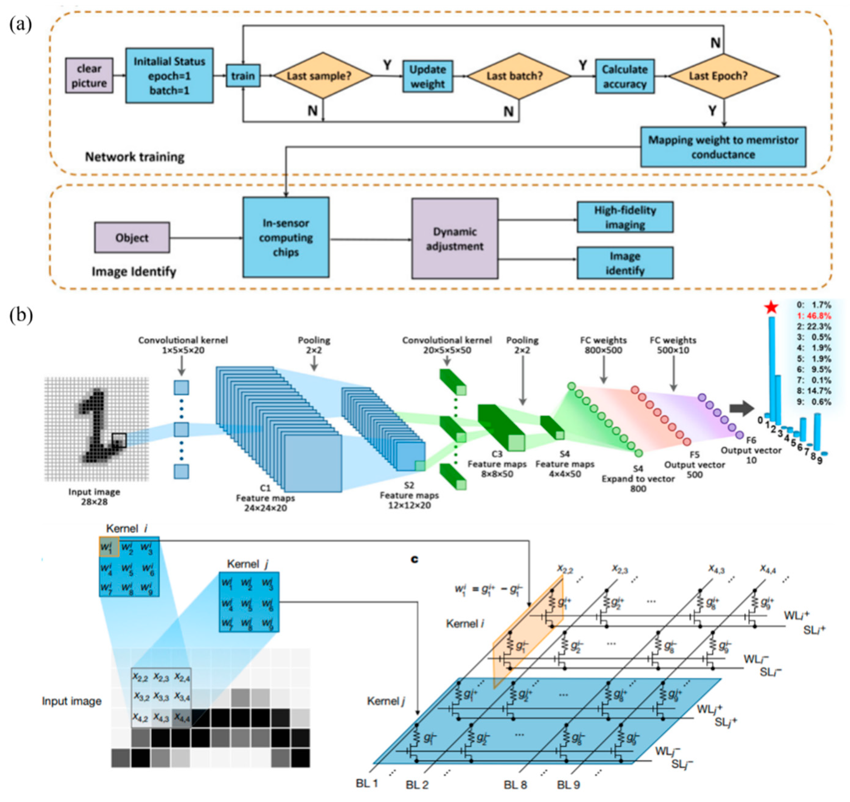
4.3. In-Memory Computing Chips
5. Conclusions and Outlook
Author Contributions
Funding
Institutional Review Board Statement
Informed Consent Statement
Data Availability Statement
Acknowledgments
Conflicts of Interest
Abbreviations
| IC | Integrated Circuits |
| CMOS | Complementary Metal Oxide Semiconductor |
| RRAM | Resistive Random Access Memory |
| HRS | High Resistance State |
| LRS | Low Resistance State |
| PCN | Pocket-Channel Framework |
| ZIF | Zeolitic Imidazolate Framework |
| BTC | Benzene-1mine-3-tricarboxylic acid |
| PET | Polyethylene Terephthalate |
| EGaIn | eutectic gallium-indium |
| GaInSn | Gallium-indium-tin |
| CP | Conductive Path |
| TE | Top Electrode |
| BE | Bottom Electrode |
| PVPy | Polyvinylpyrrolidone |
| PMMA | Poly-(methyl methacrylate) |
| PVA | Polyvinyl Alcohol |
| NAND | Not AND |
| NOR | Not OR |
| WORM | Write-Once-Read-Many |
| SCLC | Space Charge Limited Conduction |
| ECM | Electrochemical Metallization |
| CB | Conductive Bridge |
| I–V | Current Voltage Characteristic |
| STDP | Spike Timing Dependent Plasticity |
| SNN | Spiking Neural Network |
| MNIST | Mixed National Institute of Standards and Technology database |
| CNN | Convolutional Neural Networks |
References
- Chen, C.L.P.; Zhang, C.Y. Data-Inntensive Applications, Challenges, Techniques and Tehnologies: A Surgey on Big Data. Inf. Sci. 2014, 275, 314–347. [Google Scholar] [CrossRef]
- Zidan, M.A.; Strachan, J.P.; Lu, W.D. The Future of Electronics Based on Memristive Systems. Nat. Electron. 2018, 1, 22–29. [Google Scholar] [CrossRef]
- Reinsel, D.; Gantz, J.; Rydning, J. The Digitization of the World from Edge to Core; IDC White Paper; International Data Corporation (IDC): Needham, MA, USA, 2018. [Google Scholar]
- Theis, T.; Wong, H. The End of Moore’s Law: A New Beginning for Information Technology. Comput. Sci. Eng. 2017, 19, 41–50. [Google Scholar] [CrossRef]
- Track, E.; Forbes, N.; Strawn, G. The End of Moore’s Law. Comput. Sci. Eng. 2017, 19, 4–6. [Google Scholar] [CrossRef]
- Patterson, D.; Anderson, T.; Cardwell, N.; Fromm, R.; Keeton, K.; Kozyrakis, C.; Thomas, R.; Yelick, K. A Case for Intelligent RAM. IEEE Micro 1997, 17, 34–44. [Google Scholar] [CrossRef]
- Rogers, B.M.; Krishna, A.; Bell, G.B.; Jiang, X.W. Scaling the Bandwidth Wall: Challenges in and Avenues for CMP Scaling. In Proceedings of the 36th Annual International Symposium on Computer Architecture, Austin, TX, USA, 20–24 June 2009; Volume 37, pp. 371–382. [Google Scholar]
- Moore, S. Another Step toward the End of Moore’s Law. IEEE Spectr. 2019, 56, 9–10. [Google Scholar] [CrossRef]
- Strukov, D.B.; Snider, G.S.; Stewart, D.R.; Williams, R.S. The Missing Memristor Found. Nature 2008, 453, 80–83. [Google Scholar] [CrossRef]
- Chua, L. Memristor—The Missing Circuit Element. IEEE Trans. Circuit Theory 1971, 18, 507–519. [Google Scholar] [CrossRef]
- Chen, Q.L.; Zhang, Y.; Liu, S.Z.; Han, T.T.; Chen, X.H.; Xu, Y.Q.; Meng, Z.Q.; Zhang, G.L.; Zheng, X.J.; Zhao, J.J.; et al. Switchable Perovskite Photovoltaic Sensors for Bioinspired Adaptive Machine Vision. Adv. Intell. Syst. 2020, 2, 20001222. [Google Scholar] [CrossRef]
- Chen, Q.L.; Han, T.T.; Tang, M.H.; Zhang, Z.; Zheng, X.J.; Liu, G. Improving the Recognition Accuracy of Memristive Neural Networks via Homogenized Analog Type Conductance Quantization. Micromachines 2020, 11, 427. [Google Scholar] [CrossRef]
- Chen, Q.L.; Liu, G.; Xue, W.H.; Shang, J.; Gao, S.; Yi, X.; Lu, Y.; Chen, X.H.; Tang, M.H.; Zheng, X.J.; et al. Controlled Construction of Atomic Point Contact with 16 Quantized Conductance States in Oxide Resistive Switching Memory. ACS Appl. Electron. Mater. 2019, 1, 789–798. [Google Scholar] [CrossRef]
- Ali, K.A.; Rizk, M.; Baghdadi, A.; Diguet, J.P.; Jomaah, J. Crossbar Memory Architecture Performing Memristor Overwrite Logic. In Proceedings of the 2019 26th IEEE International Conference on Electronics, Circuits and Systems (ICECS), Genoa, Italy, 27–29 November 2019. [Google Scholar]
- Luo, L.; Dong, Z.K.; Duan, S.K.; Lai, C.S. Memristorbased Stateful Logic Gates for Multi-Functional Logic Circuit. IET Circuits Devices Syst. 2020, 14, 811–818. [Google Scholar] [CrossRef]
- Huo, Q.; Yang, Y.M.; Wang, Y.M.; Lei, D.Y.; Fu, X.Q.; Ren, Q.R.; Xu, X.X.; Luo, Q.; Xing, G.Z.; Chen, C.Y.; et al. Computing-in-Memory Macro Based on Three-Dimensional Resistive Random-Access Memory. Nat. Electron. 2022, 5, 469–477. [Google Scholar] [CrossRef]
- Wan, W.; Kubendran, R.; Schaefer, C.; Eryilmaz, S.B.; Zhang, W.Q.; Wu, D.; Deiss, S.; Raina, P.; Qian, H.; Gao, B.; et al. A Compute-in-Memory Chip Based on Resistive Random-Access Memory. Nature 2022, 608, 504–512. [Google Scholar] [CrossRef]
- Zhang, B.; Chen, W.L.; Zeng, J.M.; Fan, F.; Gu, J.W.; Chen, X.H.; Yan, L.; Xie, G.J.; Liu, S.Z.; Yan, Q.; et al. 90% Yield Production of Polymer Nanomemristor for In-Memory Computing. Nat. Commun. 2021, 12, 1984. [Google Scholar] [CrossRef]
- Kumar, P.; Zhu, K.; Gao, X.; Wang, S.D.; Lanza, M.; Thakur, C.S. Hybrid Architecture Based on Two-Dimensional Memristor Crossbar Array and CMOS Integrated Circuit for Edge Computing. NPJ 2D Mater. Appl. 2022, 6, 8. [Google Scholar] [CrossRef]
- Khan, M.; Kim, J.; Chougale, M.Y.; Furqan, C.M.; Saqib, Q.M.; Shaukat, R.A.; Kobayashi, N.P.; Mohammad, B.; Bae, J.; Kwok, H. Ionic Liquid Multistate Resistive Switching Characteristics in Two Terminal Soft and Flexible Discrete Channels for Neuromorphic Computing. Microsyst. Nanoeng. 2022, 8, 56. [Google Scholar] [CrossRef]
- Li, Y.; Zhang, Z.; Li, J.; Chen, X.D.; Kong, Y.; Wang, F.D.; Zhang, G.X.; Lu, T.B.; Zhang, J. Low-Voltage Ultrafast Nonvolatile Memory Via Direct Charge Injection Through a Threshold Resistive-Switching Layer. Nat. Commun. 2022, 13, 4591. [Google Scholar] [CrossRef]
- Stiff-Roberts, A.; Ge, W. Organic/Hybrid Thin Films Deposited by Matrix-Assisted Pulsed Laser Evaporation (Maple). Appl. Phys. Rev. 2017, 4, 041303. [Google Scholar] [CrossRef]
- Rullyani, C.; Ramesh, M.; Sung, C. Natural Polymers for Disposable Organic Thin Film Transistors. Org. Electron. 2018, 54, 154–160. [Google Scholar] [CrossRef]
- Kang, J.; Kim, T.; Hu, S.; Kim, J.; Kwak, J.Y.; Par, J.; Park, J.K.; Kim, I.; Lee, S.; Kim, S.; et al. Cluster-Type Analogue Memristor by Engineering Redox Dynamics for High-Performance Neuromorphic Computing. Nat. Commun. 2022, 13, 40. [Google Scholar] [CrossRef]
- Park, S.; Jeong, H.; Park, J.; Bae, J.; Choi, S. Experimental Demonstration of Highly Reliable Dynamic Memristor for Artificial Neuron and Neuromorphic Computing. Nat. Commun. 2022, 13, 28–88. [Google Scholar] [CrossRef]
- Sun, K.; Chen, J.; Yan, X. The Future of Memristors: Materials Engineering and Neural Networks. Adv. Funct. Mater. 2021, 31, 2006773. [Google Scholar] [CrossRef]
- Yuan, L.; Liu, S.Z.; Chen, W.L. Organic Memory and Memristors: From Mechanisms, Materials to Devices. Adv. Mater. 2021, 7, 2100432. [Google Scholar] [CrossRef]
- Lollar, C.; Qin, J.; Pang, J.; Yuan, S.; Becker, B.; Zhou, H. Interior Decoration of Stable Metal-Organic Frameworks. Langmuir 2018, 34, 13795–13807. [Google Scholar] [CrossRef]
- Allendorf, M.; Schwartzberg, A.; Stavila, V.; Talin, A.A. A Roadmap to Implementing Metal-Organic Frameworks in Electronic Devices: Challenges and Critical Directions. Eur. J. 2011, 17, 11372–11388. [Google Scholar] [CrossRef]
- Stassen, I.; Burtch, N.; Talin, A.; Falcaro, P.; Allendorf, M.; Ameloot, R. An Updated Roadmap for The Integration of Metal-Organic Frameworks with Electronic Devices and Chemical Sensors. Chem. Soc. Rev. 2017, 46, 3185–3241. [Google Scholar] [CrossRef]
- Batten, S.; Champness, N.; Chen, X. Terminology of Metal-Organic Frameworks and Coordination Polymers. Pure Appl. Chem. 2013, 85, 1715–1724. [Google Scholar] [CrossRef] [Green Version]
- Takaishi, S.; Hosoda, M.; Kajiwara, T.; Miyasaka, H.; Yamashita, M.; Nakanishi, Y.; Kitagawa, Y.; Yamaguchi, K.; Kobayashi, A.; Kitagawa, H. Electroconductive Porous Coordination Polymer Cu[Cu(pdt)2] Composed of Donor and Acceptor Building Units. Inorg. Chem. 2009, 48, 9048–9050. [Google Scholar] [CrossRef]
- Kobayashi, Y.; Jacobs, B.; Allendorf, M.; Long, J. Conductivity, Doping, and Redox Chemistry of a Microporous Dithiolene-Based Metal-Organic Framework. Chem. Mater. 2010, 22, 4120–4122. [Google Scholar] [CrossRef]
- Alessandro, D.; Kanga, J.; Caddy, J. Towards Conducting Metal-Organic Frameworks. Aust. J. Chem. 2011, 64, 718–722. [Google Scholar] [CrossRef]
- Yoon, S.; Warren, S.; Grzybowski, B. Storage of Electrical Information in Metal-Organic-Framework Memristors. Angew. Chem. Int. Ed. 2014, 53, 4437–4441. [Google Scholar] [CrossRef]
- Feldblyum, J.; McCreery, C.; Andrews, S.; Kurosawa, T. Few-Layer, Large-Area, 2D Covalent Organic Framework Semiconductor Thin Films. Chem. Commun. 2015, 51, 13894–13897. [Google Scholar] [CrossRef]
- Xie, L.; Skorupskii, G.; Dinca, M. Electrically Conductive Metal-Organic Frameworks. Chem. Rev. 2020, 120, 8536–8580. [Google Scholar] [CrossRef] [Green Version]
- Chen, A.; Haddad, S.; Wu, Y.C.; Fang, T.N.; Lan, Z.; Avanzino, S.; Pangrle, S.; Buynoski, M.; Rathor, M.; Cai, W.; et al. Non-volatile resistive switching for advanced memory applications. In Proceedings of the International Electron Devices Meeting 2005 (IEDM) Technical Digest, Washington, DC, USA, 2–5 December 2005. [Google Scholar]
- Onlaor, K.; Thiwawong, T.; Tunhoo, B. Electrical switching and conduction mechanisms of nonvolatile write-once-read-many-times memory devices with ZnO nanoparticles embedded in polyvinylpyrrolidone. Org. Electron. 2016, 31, 19. [Google Scholar] [CrossRef]
- Wang, Y.; Lv, Z.; Liao, Q.; Shan, H.; Chen, J.; Zhou, Y.; Zhou, L.; Chen, X.; Roy, V.A.L.; Wang, Z.; et al. Synergies of Electrochemical Metallization and Valance Change in All-Inorganic Perovskite Quantum Dots for Resistive Switching. Adv. Mater. 2018, 30, 1800327. [Google Scholar] [CrossRef]
- Rehman, M.M.; Siddiqui, G.U.; Gul, J.Z.; Kim, S.W.; Lim, J.H.; Choi, K.H. Resistive Switching in All-Printed, Flexible and Hybrid MoS2-PVA Nanocomposite based Memristive Device Fabricated by Reverse Offset. Sci. Rep. 2016, 6, 36195. [Google Scholar] [CrossRef]
- Qian, K.; Tay, R.Y.; Nguyen, V.C.; Wang, J.; Cai, G.; Chen, T.; Teo, E.H.T.; Lee, P.S. Hexagonal Boron Nitride Thin Film for Flexible Resistive Memory Applications. Adv. Funct. Mater. 2016, 26, 2176. [Google Scholar] [CrossRef]
- Hosseini, N.R.; Lee, J.S. Biocompatible and Flexible Chitosan-Based Resistive Switching Memory with Magnesium Electrodes. Adv. Funct. Mater. 2015, 25, 5586. [Google Scholar] [CrossRef]
- Huang, Y.R.; Lin, X.L.; Chen, B.; Zheng, H.D.; Chen, Z.R.; Li, H.H.; Zheng, S.T. Thermal-Responsive Polyoxometalate–Metalloviologen Hybrid: Reversible Intermolecular Three-Component Reaction and Temperature-Regulated Resistive Switching Behaviors. Angew. Chem. Int. Ed. 2021, 60, 16911–16916. [Google Scholar] [CrossRef]
- Gallegos, I.R.; Niño, J.Á.; Arriaga, D.H.; Reyes, M.R.; Sandoval, R.L. Flexible Rewritable Organic Memory Devices Using Nitrogen-Doped CNTs/PEDOT: PSS Composites. Org. Electron. 2017, 45, 159. [Google Scholar] [CrossRef]
- Cheng, X.F.; Shi, E.B.; Hou, X.; Shu, J.; He, J.H.; Li, H.; Xu, Q.F.; Li, N.J.; Chen, D.Y.; Lu, J.M. 1D π-d Conjugated Coordination Polymers for Multilevel Memory of Long-Term and High-Temperature Stability. Adv. Electron. Mater. 2017, 3, 1700107. [Google Scholar] [CrossRef]
- He, K.; Liu, Y.; Wang, M.; Chen, G.; Jiang, Y.; Yu, J.; Wan, C.; Qi, D.; Xiao, M.; Leow, W.R.; et al. An Artificial Somatic Reflex Arc. Adv. Mater. 2020, 32, 1905399. [Google Scholar] [CrossRef] [PubMed]
- Cavka, J.H.; Jakosen, S.; Olsbye, U.; Guillou, N.; Lamberti, C.; Bordiga, S.; Lillerud, K.P. A New Zirconium Inorganic Building Brick Forming Metal Organic Frameworks with Exceptional Stability. J. Am. Chem. Soc. 2008, 130, 13850–13851. [Google Scholar] [CrossRef] [PubMed]
- Liu, Y.; Wang, H.; Shi, W.X.; Zhang, W.N.; Yu, J.C.; Chandran, B.K.; Cui, C.L.; Zhu, B.; Liu, Z.Y.; Li, B.; et al. Alcohol-Mediated Resistance-Switching Behavior in Metal-Organic Framework-Based Electronic Devices. Angew. Chem. Int. Ed. 2016, 55, 8884–8888. [Google Scholar] [CrossRef]
- Yao, Z.Z.; Pan, L.; Liu, L.Z.; Zhang, J.D.; Lin, Q.J.; Ye, Y.X.; Zhang, Z.J.; Xiang, S.C.; Chen, B.L. Simultaneous Implementation of Resistive Switching and Rectifying Effects in A Metal-Organic Framework with Switched Hydrogen Bond Pathway. Sci. Adv. 2019, 5, 4515. [Google Scholar] [CrossRef] [Green Version]
- Pan, L.; Liu, G.; Li, H.; Meng, S.; Han, L.; Shang, J.; Chen, B.; Prats, A.E.P.; Lu, W.; Zou, X.D.; et al. A Resistance-Switchable and Ferroelectric Metal-Organic Framework. J. Am. Chem. Soc. 2014, 136, 17477–17483. [Google Scholar] [CrossRef]
- Chen, L.; Gong, Q.; Chen, Z. Preparation and Application of Ultra-Thin Two Dimensional MOF Nanomaterials. Prog. Chem. 2021, 33, 1280–1292. [Google Scholar]
- Ding, G.L.; Wang, Y.X.; Zhang, G.X.; Zhou, K.; Zeng, K.L.; Li, Z.X.; Zhou, Y.; Zhang, C.; Chen, X.L.; Han, S.T. 2D Metal-Organic Framework Nanosheets with Time-Dependent and Multilevel Memristive Switching. Adv. Funct. Mater. 2019, 29, 1806637. [Google Scholar] [CrossRef]
- Shekhah, O.; Wang, H.; Kowarik, S.; Schreiber, F.; Paulus, M.; Tolan, M.; Steremann, C.; Evers, F.; Zacher, D.; Fischer, R.A.; et al. Step-by-Step Route for the Synthesis of Metal-Organic Frameworks. J. Am. Chem. Soc. 2007, 129, 15118–15119. [Google Scholar] [CrossRef]
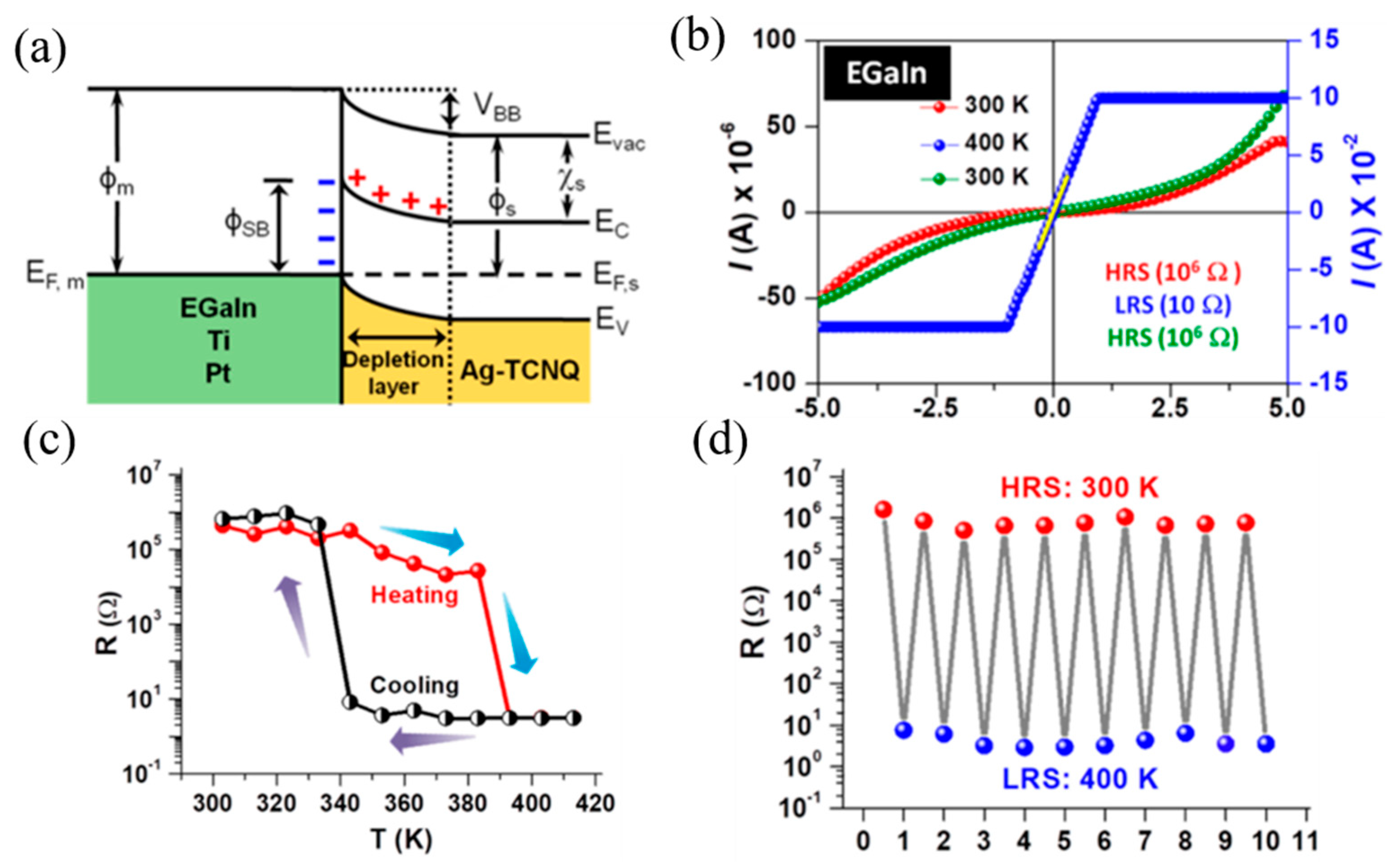
- Yi, X.H.; Yu, Z.; Niu, X.H.; Shang, J.; Mao, G.Y.; Yin, T.H.; Yang, H.L.; Xue, W.H.; Dhanapal, P.; Qu, S.X.; et al. Intrinsically Stretchable Resistive Switching Memory Enabled by Combining a Liquid Metal-Based Soft Electrode and a Metal-Organic Framework Insulator. Adv. Electron. Mater. 2019, 5, 1800655. [Google Scholar] [CrossRef]
- Albano, L.G.S.; Vello, T.P.; Camargo, D.H.S.D.; Silva, R.M.L.D.; Padilha, A.C.M.; Fazzio, A.; Bufon, C.C.B. Ambipolar Resistive Switching in an Ultrathin Surface-Supported Metal-Organic Framework Vertical Heterojunction. Nano Lett. 2020, 20, 1080–1088. [Google Scholar] [CrossRef] [PubMed]
- Wang, J.; Feng, Y.; Zhang, B. MOF-COF Hybrid Frameworks Materials. Prog. Chem. 2022, 34, 1308–1320. [Google Scholar]
- Talin, A.; Centrone, A.; Ford, A.C.; Foster, M.E.; Stavila, V.; Haney, P.; Kinney, R.A.; Szalai, V.; Gabaly, F.E.; Yoon, H.P.; et al. Tunable Electrical Conductivity in Metal-Organic Framework Thin-Film Devices. Science 2014, 343, 66–69. [Google Scholar] [CrossRef] [PubMed]
- Wang, Z.; Nminibapiel, D.; Shrestha, P.; Liu, J.; Guo, W.; Weidler, P.G.; Baumgart, H.; Wöll, C.; Redel, E. Resistive Switching Nanodevices Based on Metal-Organic Frameworks. ChemNanoMat 2016, 2, 67–73. [Google Scholar] [CrossRef]
- Tran, T.N.H.; Le, T.H.; Ta, H.K.T.; Dang, Y.T.; Nguyen, L.T.H.; Doan, T.H.L.; Fang, C.; Hwang, I.; Phan, T.B.; Pham, N.K. C-AFM Study on Multi-Resistive Switching Modes Observed in Metal-Organic Frameworks Thin Films. Org. Electron. 2021, 93, 106136. [Google Scholar] [CrossRef]
- Park, S.S.; Hontz, E.R.; Sun, L.; Hendon, C.H.; Walsh, A.; Voorhis, T.V.; Dincă, M. Cation-Dependent Intrinsic Electrical Conductivity in Isostructural Tetrathiafulvalene-Based Microporous Metal-Organic Frameworks. J. Am. Chem. Soc. 2015, 137, 1774–1777. [Google Scholar] [CrossRef] [Green Version]
- Chen, D.S.; Xing, H.Z.; Su, Z.M.; Wang, C.G. Electrical Conductivity and Electroluminescence of a New Anthracene-Based Metal-Organic Framework With P-Conjugated Zigzag Chains. Chem. Commun. 2016, 52, 2019–2022. [Google Scholar]
- Lin, K.; Adhikari, A.K.; Ku, C.N.; Chiang, C.L.; Kuo, H. Synthesis and Characterization of Porous HKUST-1 Metal Organic Frameworks for Hydrogen Storage. Int. J. Hydrogen Energy 2012, 37, 13865–13871. [Google Scholar] [CrossRef]
- Chui, S.S.Y.; Lo, S.M.F.; Charmant, J.P.H.; Orpen, A.G.; Williams, I.D. A Chemically Functionalizable Nanoporous Material [Cu3(TMA)2(H2O)3]n. Science 1999, 283, 1148–1150. [Google Scholar] [CrossRef]
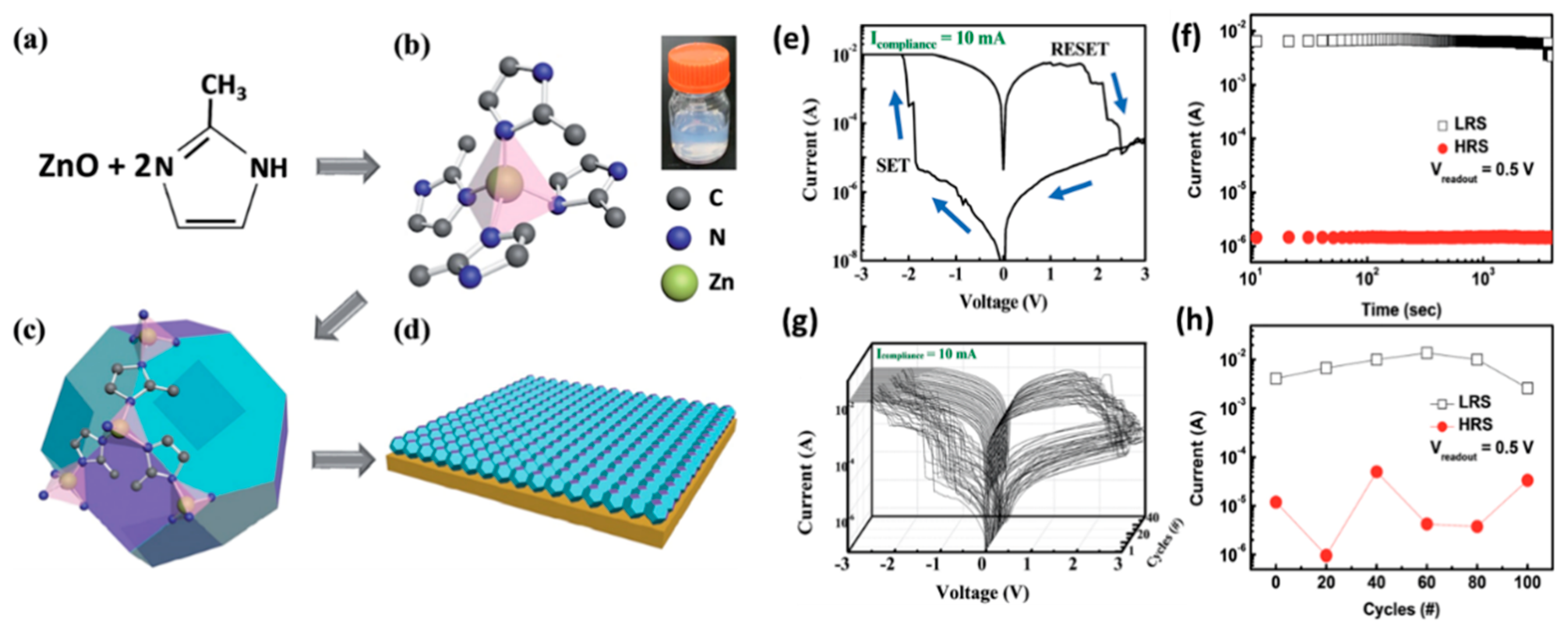
- Hayashi, H.; Côté, A.P.; Furukawa, H.; Keeffe, M.O.; Yaghi, O.M. Zeolite A Imidazolate Frameworks. Nat. Mater. 2007, 6, 501–506. [Google Scholar] [CrossRef] [PubMed]
- He, Y.; Huang, Y.R.; Li, H.H.; Chen, Z.R.; Jiang, R. Encapsulating Halometallates into 3-D Lanthanide-Viologen Frameworks: Controllable Emissions, Reversible Thermochromism, Photocurrent Responses, and Electrical Bistability Behaviors. Inorg. Chem. 2019, 58, 13862–13880. [Google Scholar] [CrossRef] [PubMed]
- Chen, B.; Huang, Y.; Song, K.; Lin, X.L.; Li, H.H.; Chen, Z.R. Molecular Nonvolatile Memory Based On [α-GeW12O49]4−/Metalloviologen Hybrids Can Work at High Temperature Monitored by Chromism. Chem. Mater. 2021, 33, 2178–2186. [Google Scholar] [CrossRef]
- Rana, S.; Prasoon, A.; Jha, P.K.; Prathamshetti, A.; Ballav, N. Thermally Driven Resistive Switching in Solution-Processable Thin Films of Coordination Polymers. J. Phys. Chem. Lett. 2017, 8, 5008–5014. [Google Scholar] [CrossRef] [PubMed]
- Zhao, M.T.; Wang, Y.X.; Ma, Q.L.; Huang, Y.; Zhang, X.; Ping, J.F.; Zhang, Z.C.; Lu, Q.P.; Yu, Y.F.; Xu, H.; et al. Ultrathin 2D Metal-Organic Framework Nanosheets. Adv. Mater. 2015, 27, 7372–7378. [Google Scholar] [CrossRef]
- Pan, L.; Ji, Z.; Yi, X.; Zhu, X.; Zhu, X.J.; Chen, X.X.; Shang, J.; Liu, G.; Li, R.W. Metal-Organic Framework Nanofilm for Mechanically Flexible Information Storage Applications. Adv. Funct. Mater. 2015, 25, 2677–2685. [Google Scholar] [CrossRef]
- Park, M.J.; Lee, J.S. Zeolitic-Imidazole Framework Thin Film-Based Flexible Resistive Switching Memory. RSC Adv. 2017, 7, 21045–21049. [Google Scholar] [CrossRef] [Green Version]
- Huang, X.; Zheng, B.; Liu, Z.; Tan, C.; Liu, J.Q.; Chen, B.; Li, H.; Chen, J.Z.; Zhang, X.; Fan, Z.X.; et al. Coating Two-Dimensional Nanomaterials with Metal-Organic Frameworks. ACS Nano 2014, 8, 8695–8701. [Google Scholar] [CrossRef]
- Zheng, N.; Masel, R.I. Rapid Production of Metal-Organic Frameworks Via Microwave-Assisted Solvothermal Synthesis. J. Am. Chem. Soc. 2006, 128, 12394–12395. [Google Scholar]
- Wang, S.Z.; McGuirk, M.; Andrea, A.; Mason, J.A.; Mirkin, C.A. Metal-Organic Framework Nanoparticles. Adv. Mater. 2018, 30, 1800202. [Google Scholar] [CrossRef]
- Zhang, Z.P.; Nie, Y.J.; Hua, W.W.; Xu, J.X.; Ban, C.Y.; Xiu, F.; Liu, J.Q. Interfacial Synthesis of a Large-Area Coordination Polymer Membrane for Rewritable Nonvolatile Memory Devices. RSC Adv. 2020, 10, 20900–20904. [Google Scholar] [CrossRef] [PubMed]
- Kutubi, H.A.; Gascon, J.; Sudhölter, E.J.R.; Rassaei, L. Electrosynthesis of Metal–Organic Frameworks: Challenges and Opportunities. ChemElectroChem 2015, 2, 462–474. [Google Scholar] [CrossRef]
- Li, W.J.; Lü, J.; Gao, S.Y.; Li, Q.H.; Cao, R. Electrochemical preparation of metal–organic framework films for fast detection of nitro explosives. J. Mater. Chem. A 2014, 2, 19473–19478. [Google Scholar] [CrossRef]
- Alizadeh, S.; Nematollahi, D. Convergent and Divergent Paired Electrodeposition of Metal-Organic Framework Thin Films. Sci. Rep. 2019, 9, 14325. [Google Scholar] [CrossRef]
- Liu, L.; Dong, J.; Liu, J.; Liang, Q.; Song, Y.R.; Li, W.H.; Lei, S.B.; Hu, W.P. High-quality Two-Dimensional Metal-Organic Framework Nanofilms for Nonvolatile Memristive Switching. Small Struct. 2021, 2, 2000077. [Google Scholar] [CrossRef]
- Sun, L.F.; Zhang, Y.S.; Han, G.; Hwang, G.; Jiang, J.B.; Joo, B.; Watanabe, K.; Taniguchi, T.; Kim, Y.M.; Yu, W.J.; et al. Self-Selective Van Der Waals Heterostructures for Large Scale Memory Array. Nat. Commun. 2019, 10, 3161. [Google Scholar] [CrossRef] [Green Version]
- Vu, Q.A.; Kim, H.; Nguyen, V.L.; Won, U.Y.; Adhikari, S.; Kim, K.; Lee, Y.H.; Yu, W.J. A High-On/Off-Ratio Floating-Gate Memristor Array on A Flexible Substrate Via CVD-Grown Large-Area 2D Layer Stacking. Adv. Mater. 2017, 29, 1703363. [Google Scholar] [CrossRef]
- Yu, Z.; Shang, J.; Niu, X.H.; Liu, Y.W.; Liu, G.; Dhanapal, P.; Zheng, Y.N.; Yang, H.L.; Wu, Y.Z.; Zhou, Y.L.; et al. A Composite Elastic Conductor with High Dynamic Stability Based on 3D-Calabash Bunch Conductive Network Structure for Wearable Devices. Adv. Electron. Mater. 2018, 4, 1800137. [Google Scholar] [CrossRef]
- Yu, Z.; Ying, W.B.; Pravarthanaac, D.; Li, Y.Y.; Mao, G.Y.; Liu, Y.W.; Hu, C.; Zhang, W.X.; He, P.X.; Zhong, Z.C.; et al. Stretchable tactile sensor with high sensitivity and dynamic stability based on vertically aligned urchin-shaped nanoparticles. Mater. Today Phys. 2020, 14, 100219. [Google Scholar] [CrossRef]
- Lee, B.H.; Dong, L.I.; Bae, H.; Seong, H.; Jeon, S.B.; Seol, M.L.; Han, J.W.; Meyyappan, M.; Im, S.G.; Choi, Y.K. Foldable and Disposable Memory on Paper. Sci. Rep. 2016, 6, 38389. [Google Scholar] [CrossRef] [Green Version]
- Kulachenkov, N.; Haar, Q.; Yankin, A.; Pierson, J.F.; Nominé, A.; Milichko, V.A. MOF-Based Sustainable Memory Devices. Adv. Funct. Mater. 2021, 32, 2107949. [Google Scholar] [CrossRef]
- Prezioso, M.; Merrikh-Bayat, F.; Hoskins, B.D.; Adam, G.C.; Likharev, K.K.; Stukov, D.B. Training and Operation of an Integrated Neuromorphic Network Based on Metal-Oxide Memristors. Nature 2015, 521, 61–64. [Google Scholar] [CrossRef] [PubMed] [Green Version]
- Li, Z.W.; Chen, P.Y.; Xu, H.; Yu, S.M. Design of Ternary Neural Nnetwork with 3-D Vertical RRAM Array. IEEE Trans. Electron. Devices 2017, 64, 2721. [Google Scholar] [CrossRef]
- Kim, B.; Li, H. Leveraging 3D Vertical RRAM to Developing Neuromorphic Architecture for Pattern Classification. In Proceedings of the 2020 IEEE Computer Society Annual Symposium on VLSI (ISVLSI), Limassol, Cyprus, 6–8 July 2020. [Google Scholar]
- Xiao, T.P.; Bennett, C.H.; Feinberg, B.; Agarwal, S.; Marinella, M.J. Analog Architectures for Neural Network Acceleration Based on Non-Volatile Memory. Appl. Phys. Rev. 2020, 7, 031301. [Google Scholar] [CrossRef]
- Wang, I.T.; Lin, Y.C.; Wang, Y.F.; Hsu, C.W.; Hou, T.H. 3D Synaptic Architecture with Ultralow Sub-10 fJ Energy Per Spike for Neuromorphic Computation. In Proceedings of the 2014 IEEE International Electron Devices Meeting, San Francisco, CA, USA, 15–17 December 2014. [Google Scholar]
- Gao, B.; Bi, Y.J.; Chen, H.Y.; Liu, R.; Huang, P.; Chen, B.; Liu, L.F.; Liu, X.Y.; Yu, S.M.; Wong, H.S.P.; et al. Ultra-Low-Energy Three-Dimensional Oxide-Based Electronic Synapses for Implementation of Robust High-Accuracy Neuromorphic Computation Systems. ACS Nano 2014, 8, 6998. [Google Scholar] [CrossRef]
- Li, H.T.; Li, K.S.; Lin, C.H.; Hsu, J.L.; Chiu, W.C.; Chen, M.C.; Wu, T.T.; Sohn, J.; Eryilmaz, S.B.; Shieh, J.M.; et al. Four-Layer 3D Vertical RRAM Integrated with FinFET as a Versatile Computing Unit for Brain-Inspired Cognitive Information Processing. In Proceedings of the 2016 IEEE Symposium on VLSI Technology, Honolulu, HI, USA, 14–16 June 2016. [Google Scholar]
- Lin, P.; Li, C.; Wang, Z.R.; Li, Y.N.; Jiang, H.; Song, W.H.; Rao, M.Y.; Zhuo, Y.; Upadhyay, N.K.; Barnell, M.; et al. Three-Dimensional Memristor Circuits as Complex Neural Networks. Nat. Electron. 2020, 3, 225. [Google Scholar] [CrossRef]
- Xie, P.S.; Huang, Y.L.; Wang, W.; Meng, Y.; Lai, Z.; Wang, F.; Yip, S.P.; Bu, X.; Wang, W.J.; Li, D.J.; et al. Ferroelectric P (VDF-Trfe) Wrapped Ingaas Nanowires for Ultralow-Power Artificial Synapses. Nano Energy 2022, 91, 106654. [Google Scholar] [CrossRef]
- Ni, Y.; Feng, J.L.; Liu, J.Q.; Yu, H.; Wei, H.H.; Du, Y.; Liu, L.; Sun, L.; Zhou, J.L.; Xu, W.T. An Artificial Nerve Capable of UV-Perception, NIR-Vis Switchable Plasticity Modulation, and Motion State Monitoring. Adv. Sci. 2022, 9, 2102036. [Google Scholar] [CrossRef]
- Kim, S.W.; Jeong, Y.J.; Bidenko, P.; Lim, H.R.; Jeon, Y.R.; Kim, H.; Lee, Y.J.; Geum, D.M.; Han, J.H.; Choi, C.; et al. 3D Stackable Synaptic Transistor for 3D Integrated Artificial Neural Networks. ACS Appl. Mater. Interfaces 2020, 12, 7372–7380. [Google Scholar] [CrossRef]
- Choi, Y.; Oh, S.; Qian, C.; Park, J.H.; Cho, J.H. Vertical Organic Synapse Expandable to 3D Crossbar Array. Nat. Commun. 2020, 11, 4595. [Google Scholar] [CrossRef]
- Lian, H.; Cheng, X.Z.; Hao, H.T.; Han, J.B.; Lau, M.T.; Li, Z.; Zhou, Z.; Dong, Q.C.; Wong, W.Y. Metal-Containing Organic Compounds for Memory and Data Storage Applications. Chem. Soc. Rev. 2022, 51, 1926–1982. [Google Scholar] [CrossRef] [PubMed]
- Wang, Y.; Yang, R.; Deng, Q.; Fan, C.; Zhang, S.; Yan, Y. Application of Bimetallic MOFs and Their Derivatives in Electrochemical Energy Storage. Prog. Chem. 2022, 34, 460–473. [Google Scholar]
- Xie, L.H.; Ling, Q.D.; Hou, X.Y.; Huang, W. An Effective Friedel-Crafts Postfunctionalization of Poly(N-vinylcarbazole) to Tune Carrier Transportation of Supramolecular Organic Semiconductors Based on π-Stacked Polymers for Nonvolatile Flash Memory Cell. J. Am. Chem. Soc. 2008, 130, 2120–2121. [Google Scholar] [CrossRef] [PubMed]
- Han, S.B.; Warren, S.C.; Yoon, S.M.; Malliakas, C.D.; Hou, X.L.; Wei, Y.H.; Kanatzidis, M.G.; Grzybowski, B.A. Tunneling Electrical Connection to the Interior of Metal-Organic Frameworks. J. Am. Chem. Soc. 2015, 137, 8169–8175. [Google Scholar] [CrossRef]
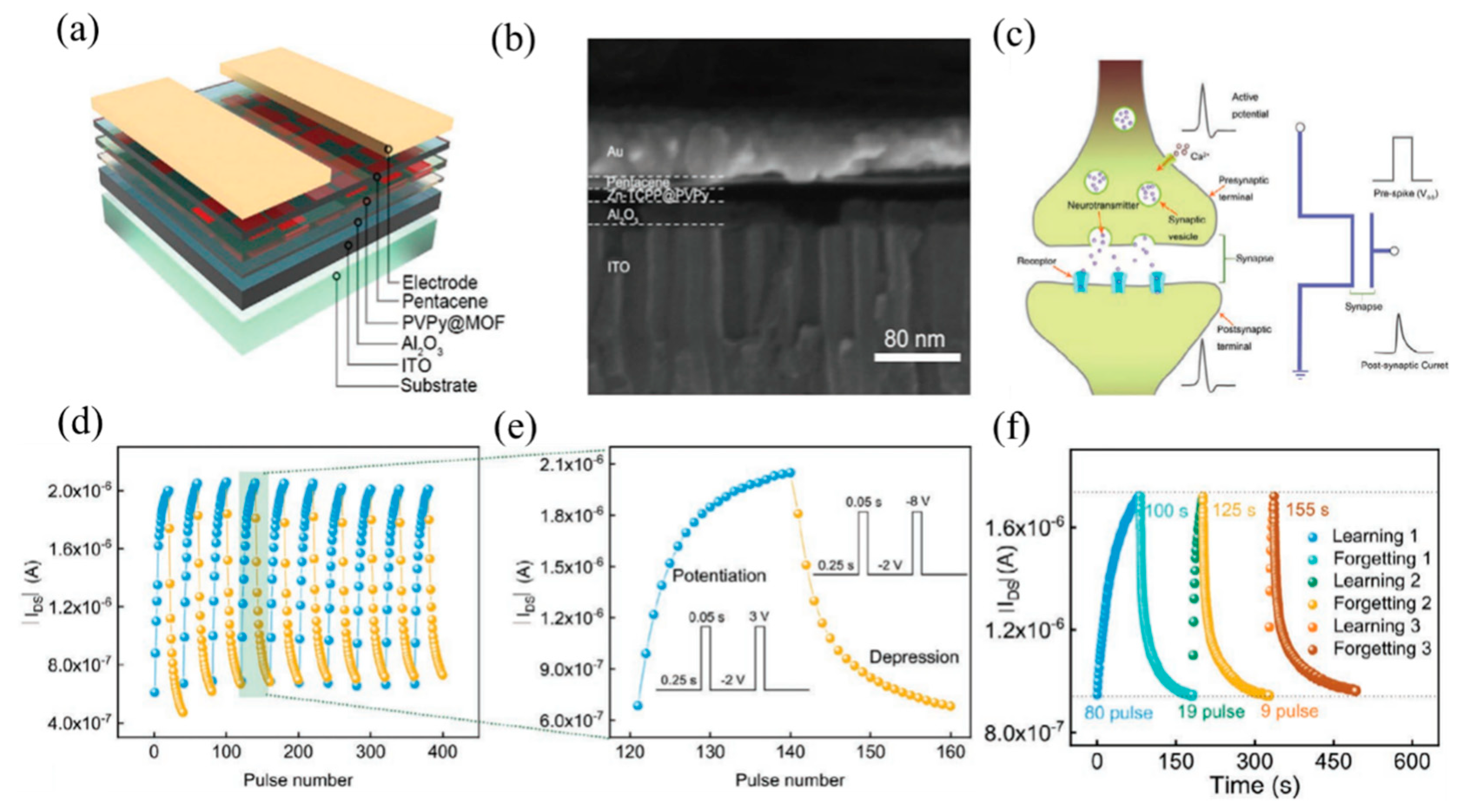
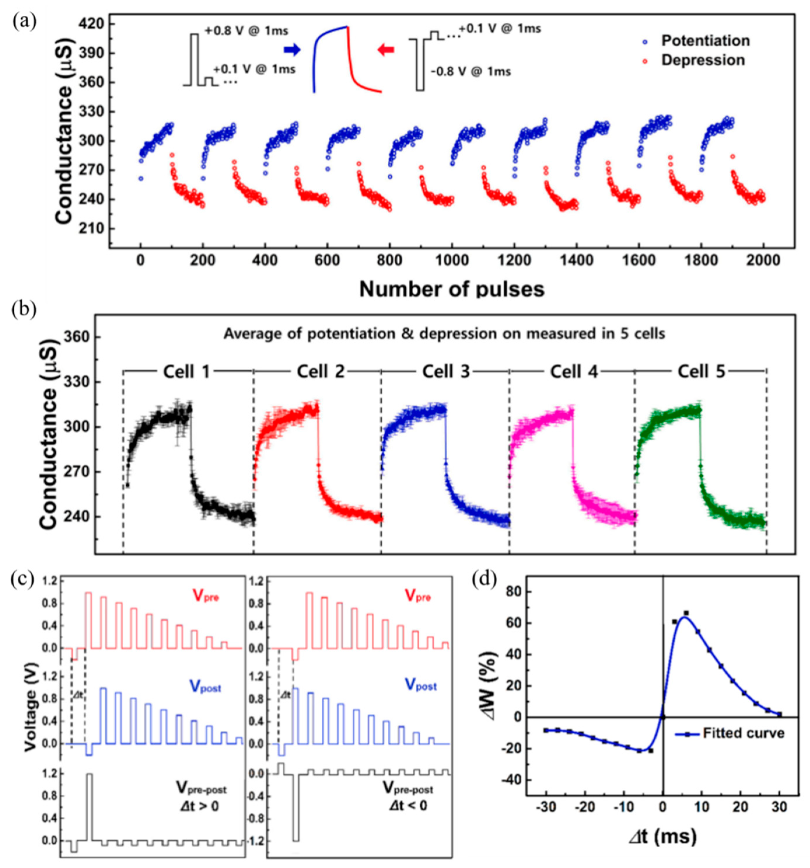
- Ding, G.L.; Yang, B.D.; Zhou, K.; Zhang, C.; Wang, Y.X.; Yang, J.Q.; Han, S.T.; Zhai, Y.B.; Roy, V.A.L.; Zhou, Y. Synaptic Plasticity and Filtering Emulated in Metal-Organic Frameworks Nanosheets Based Transistors. Adv. Electron. Mater. 2020, 6, 1900978. [Google Scholar] [CrossRef]
- Jeon, Y.J.; An, H.; Kim, Y.; Jeon, Y.P.; Kim, T.W. Highly Reliable Memristive Devices with Synaptic Behavior Via Facilitating Ion Transport of The Zeolitic Imidazolate Framework-8 Embedded into A Polyvinylpyrrolidone Polymer Matrix. Appl. Surf. Sci. 2021, 567, 150748. [Google Scholar] [CrossRef]
- Liu, Y.X.; Wei, Y.N.; Liu, M.H.; Bai, Y.C.; Liu, G.C.; Wang, X.Y.; Shang, S.C.; Gao, W.Q.; Du, C.S.; Chen, J.Y.; et al. Two-Dimensional Metal-Organic Framework Film for Realizing Optoelectronic Synaptic Plasticity. Angew. Chem. Int. Ed. 2021, 60, 17440–17445. [Google Scholar] [CrossRef]
- Liu, S.Z.; Chen, X.H.; Liu, G. Conjugated Polymers for Information Storage and Neuromorphic Computing. Polym. Int. 2020, 70, 374–403. [Google Scholar] [CrossRef]
- Chen, Q.L.; Han, T.T.; Zeng, J.M.; He, Z.L.; Liu, Y.L.; Sun, J.L.; Tang, M.H.; Zhang, Z.; Gao, P.Q.; Liu, G. Perovskite-Based Memristor with 50-Fold Switchable Photosensitivity for In-Sensor Computing Neural Network. Nanomaterials 2022, 12, 2217. [Google Scholar] [CrossRef]
- Li, C.; Belkin, D.; Li, Y.N.; Hu, M.; Ge, N.; Jiang, H.; Montgomery, E.; Lin, P.; Wang, Z.R.; Song, W.H.; et al. Efficient and Self-Adaptive In-Situ Learning in Multilayer Memristor Neural Networks. Nat. Commun. 2018, 9, 2385. [Google Scholar] [CrossRef] [Green Version]
- Souri, Z.; Ardakani, M.M.; Alizadeh, S.; Nematollahi, D. Template-free Electrodeposition of Sponge-like Porous Polymer Interwoven with the Bi-Metallic Metal-Organic Framework and Reduced Graphene Oxide and Application in Energy Storage Device. J. Energy Storage 2022, 55, 105381. [Google Scholar] [CrossRef]
- Rahimpoor, R.; Firoozichahak, A.; Nematollahi, D.; Alizadeh, S.; Alizadeh, P.M.; Langari, A.A.A. Bio-monitoring of Non-Metabolized BTEX Compounds in Urine by Dynamic Headspace-Needle Trap Device Packed with 3D Ni/Co-BTC Bimetallic Metal-Organic Framework as an Efficient Absorbent. Microchem. J. 2021, 166, 106229. [Google Scholar] [CrossRef]


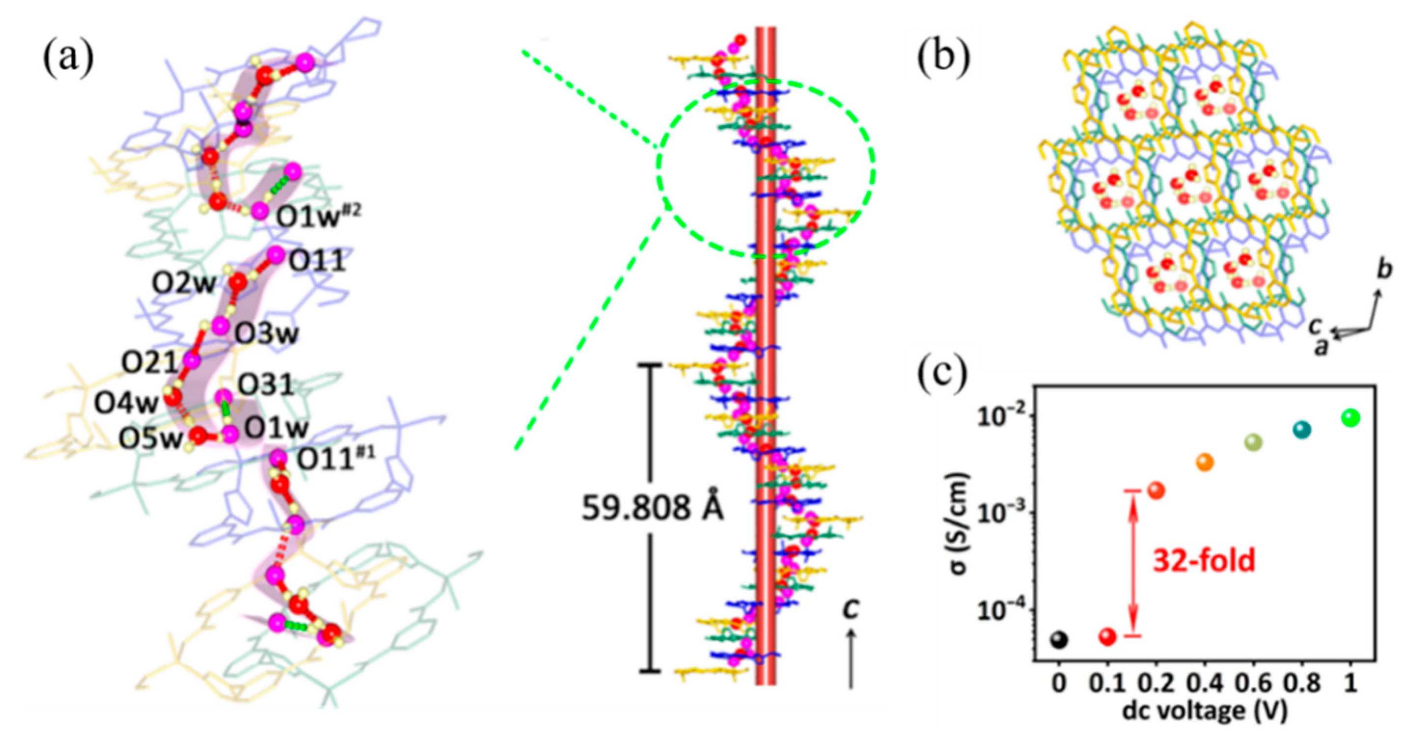
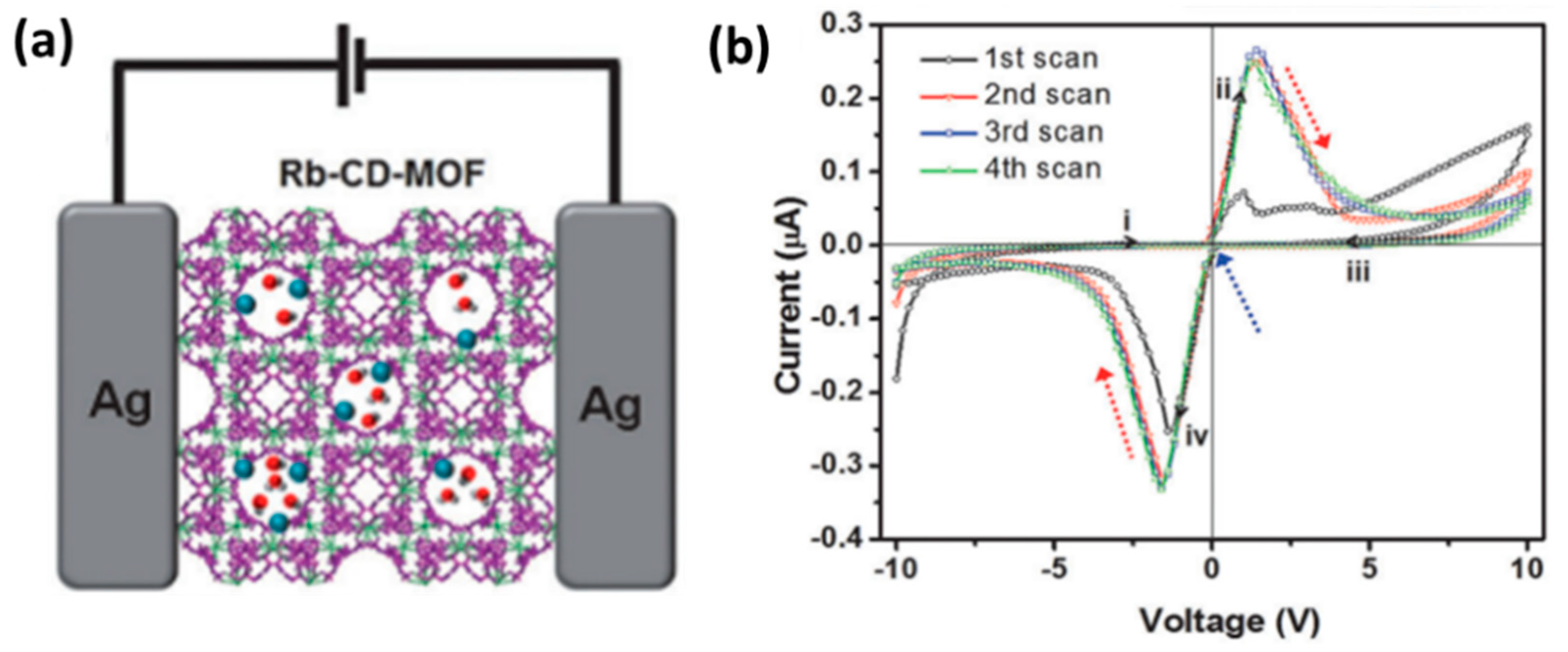
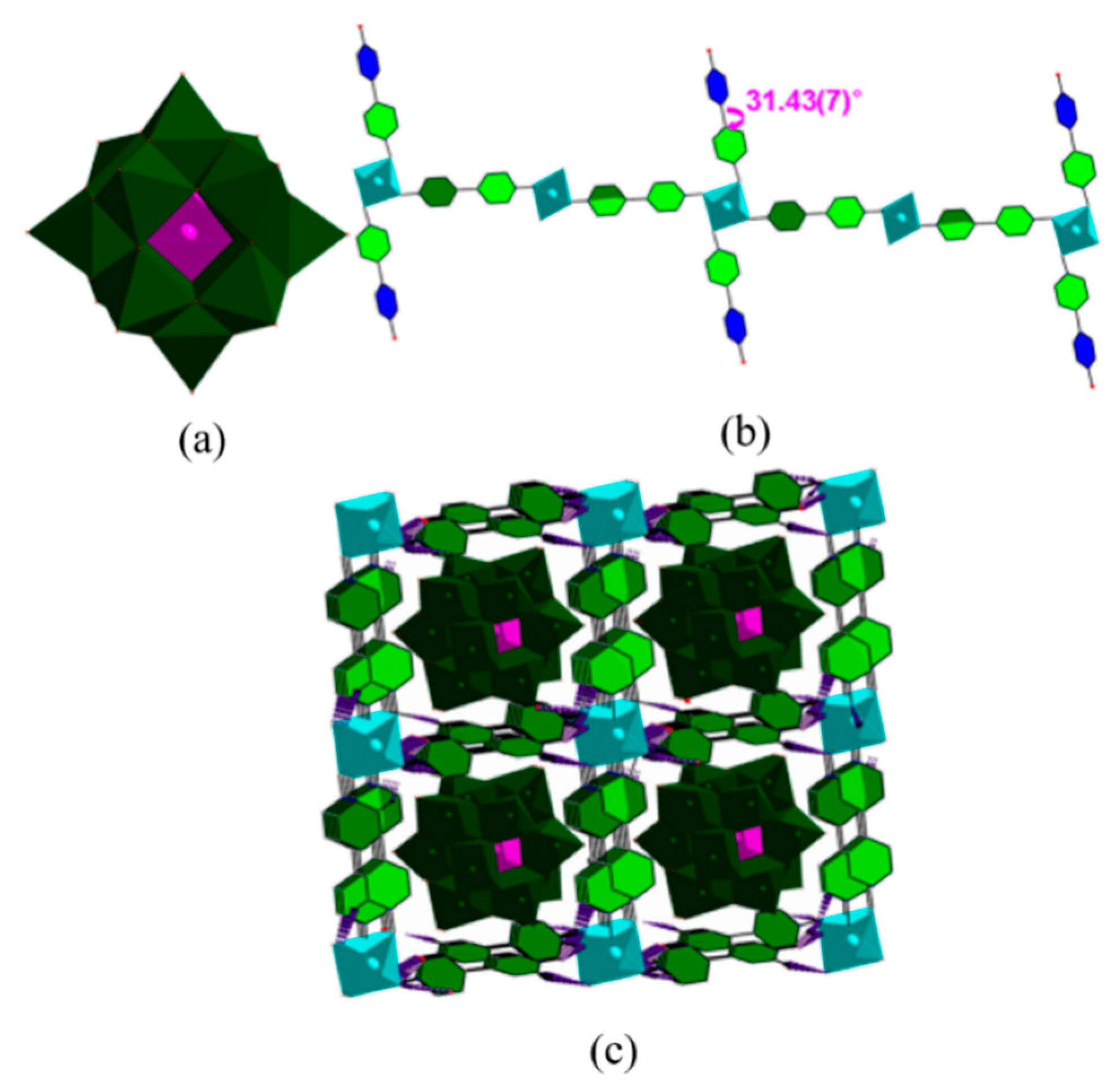
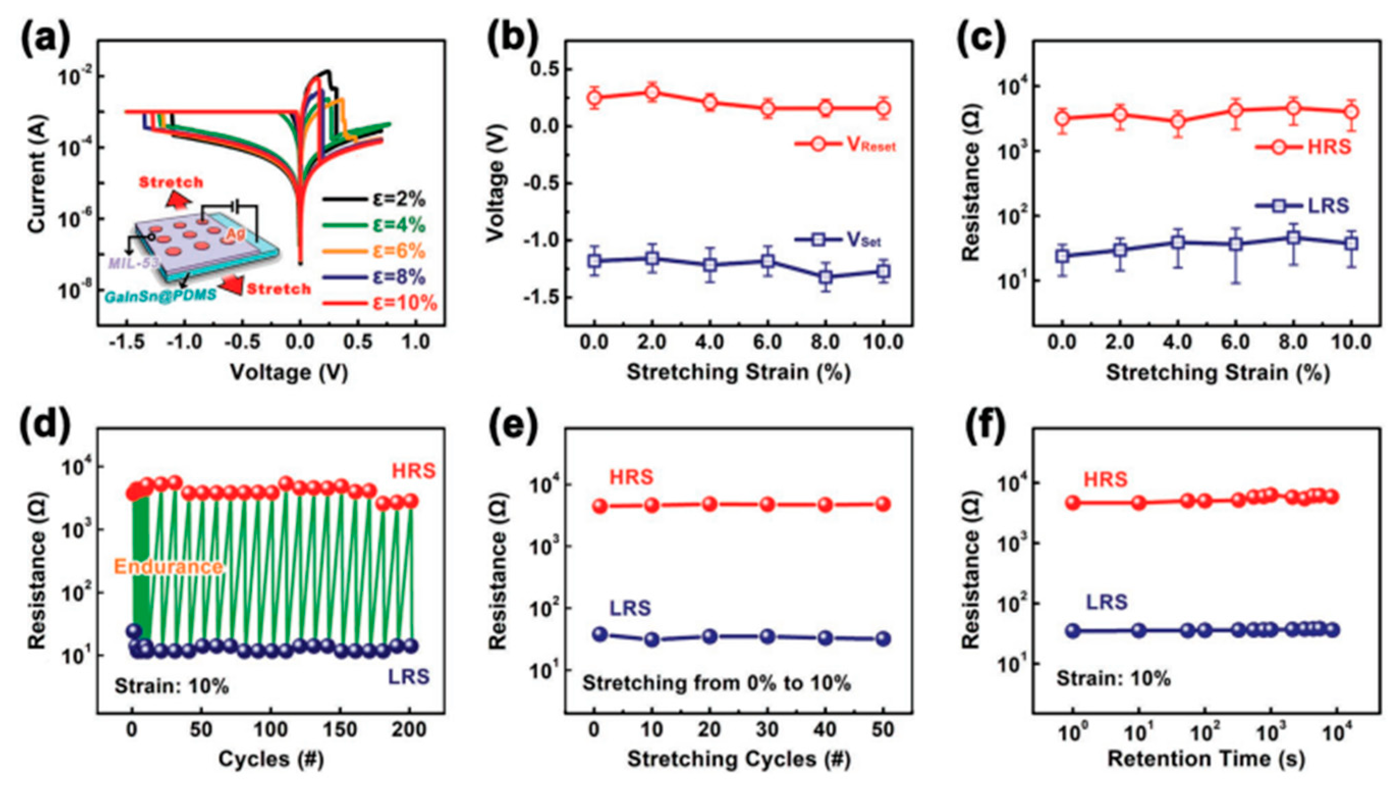
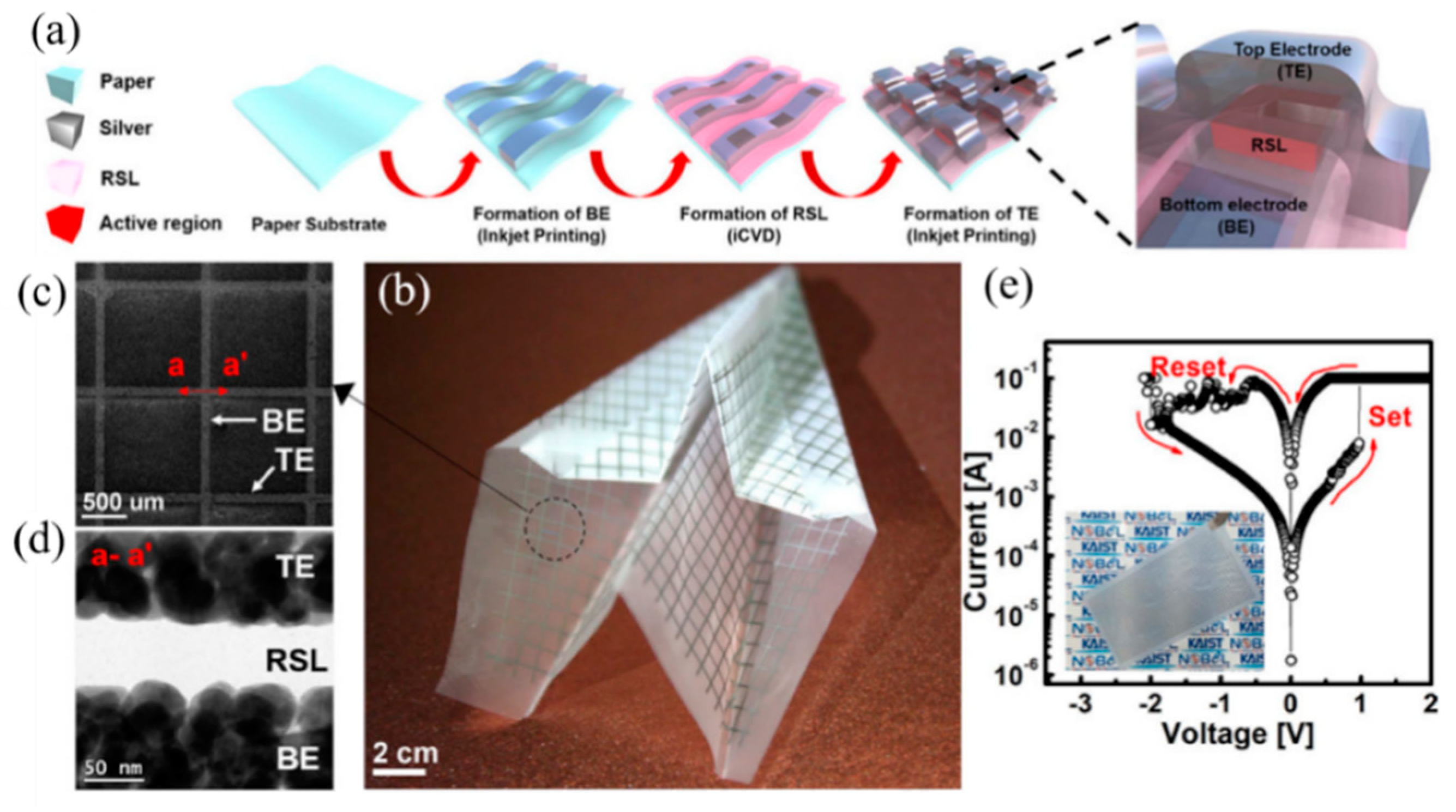
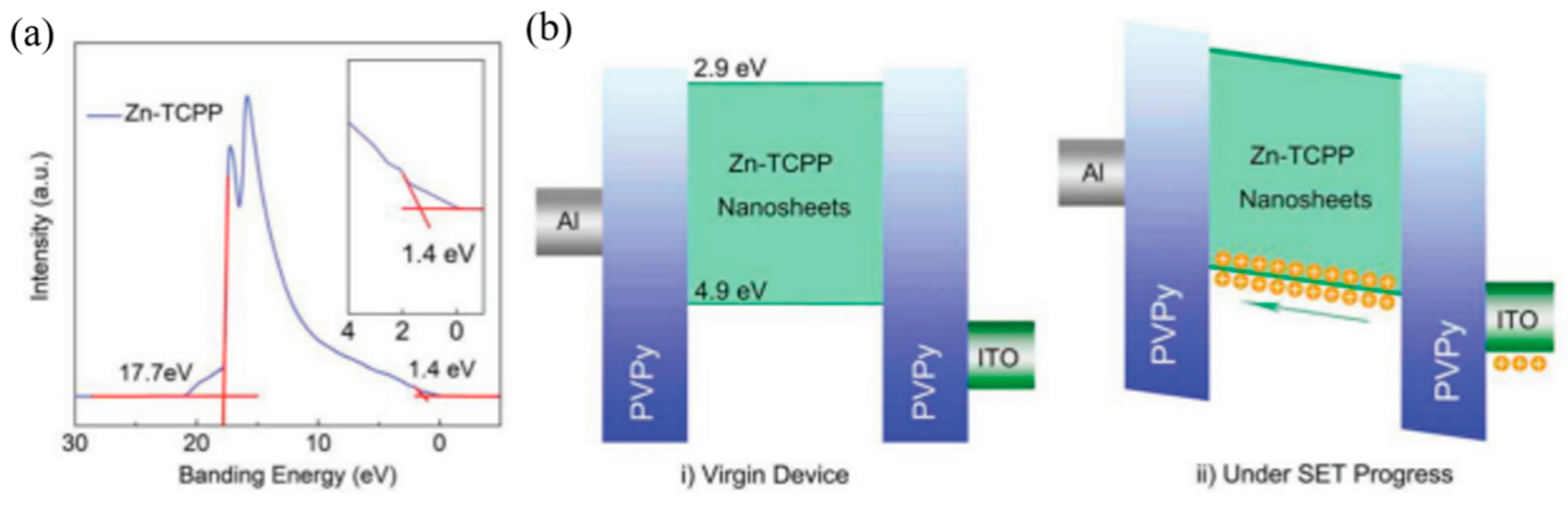
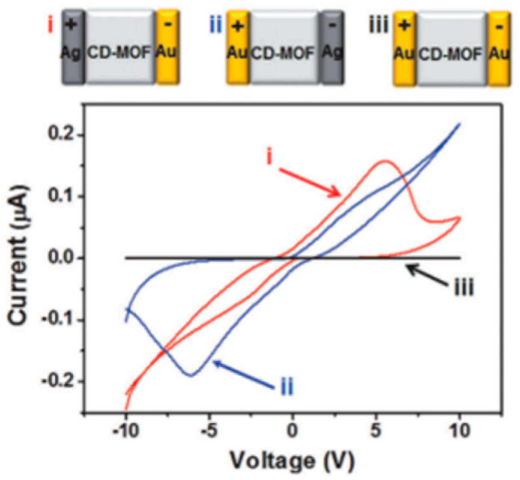
| Device Structure | Memory Effect | SET/RESET Voltage [V] | ON/OFF Ratio | Retention [s] | Endurance | Ref. |
|---|---|---|---|---|---|---|
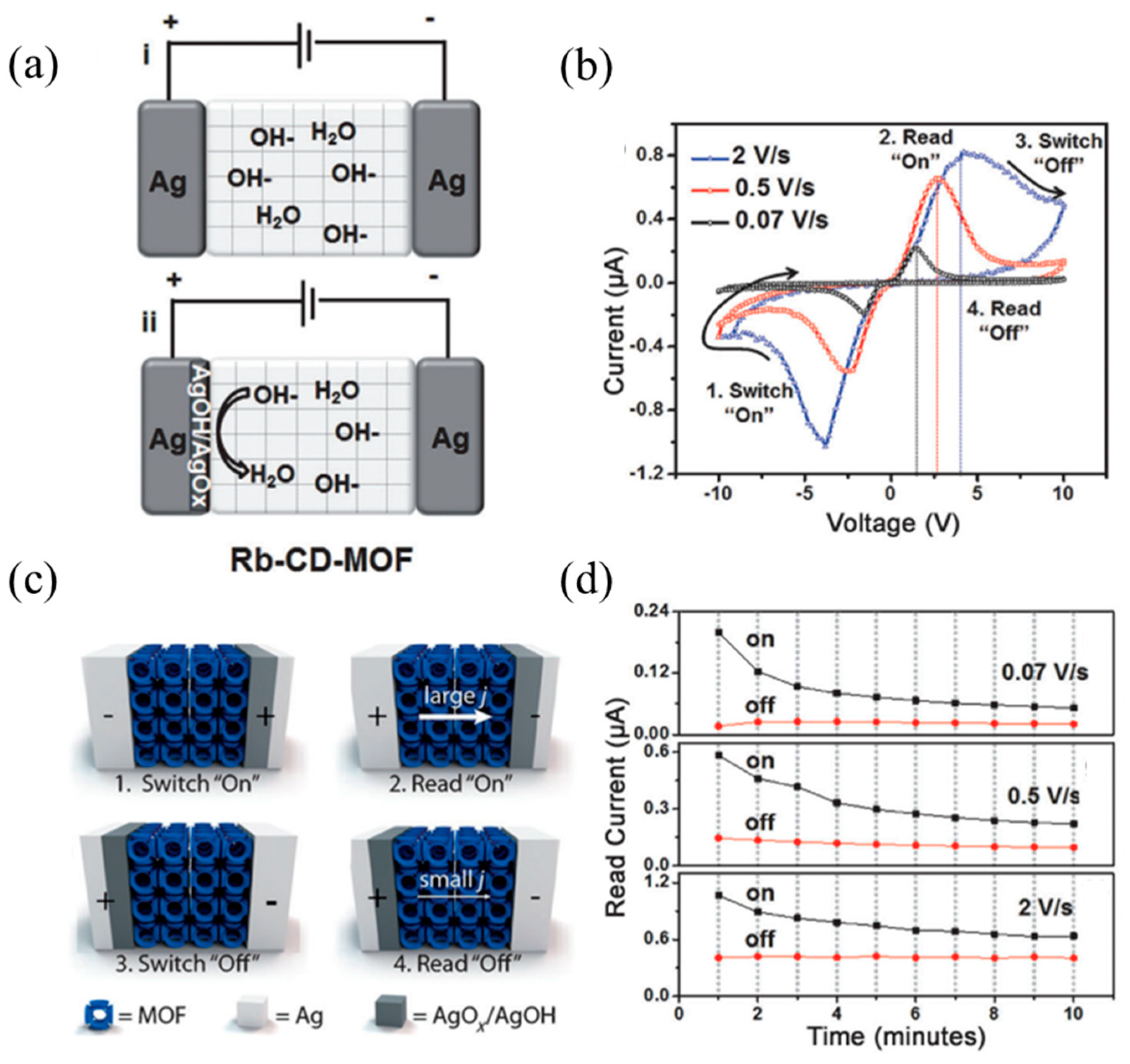
| Ag/Rb-CD-MOF/Ag | unipolar *** | ±2~4/±10 | 10 | >105 | ~20 | [35] |
| Ti/TiN/CuxO/Cu | bipolar | 2.8/1.1 | 103 | >105 | 6 × 10 | [38] |
| ITO/EVA:ZnO NPs/ITO | WORM | 4 | 103 | 4 × 10⁴ | - | [39] |
| ITO/PMMA/CsPbBr3/PMMA/Ag | bipolar | 2.6/−2.8 | 6×10⁵ | >104 | 5000 | [40] |
| Ag/h-BN/Cu foil | bipolar | 0.72/−0.37 | 1 × 10² | 3 × 10³ | 550 | [41] |
| Ag/MoS2@PVA/Ag | bipoalr | 3/−3 | 1.28 × 10² | 1 × 10⁵ | 1 × 10³ | [42] |
| Mg/Ag-doped chitosan/Mg | bipolar | 1.63/−0.82 | >102 | >104 | >60 | [43] |
| ITO/1 */Ag | bipolar | 0.52/−0.4 (270 °C) | 55.5 (270 °C) | - | - | [44] |
| Al/PEDOT: PSS-EB-NCNT/Al | bipolar | −2/3 | 103 | 1 × 10⁴ | 100 | [45] |
| ITO/Ni-BPTA/Al | unipolar | −1.65/−2.81 | 1:104:108 * | >104 | 104 | [46] |
| Ag/ZIF-8/Au/PDMS | bipolar | 3.5/−1.4 | - | 3000 | 10 | [47] |
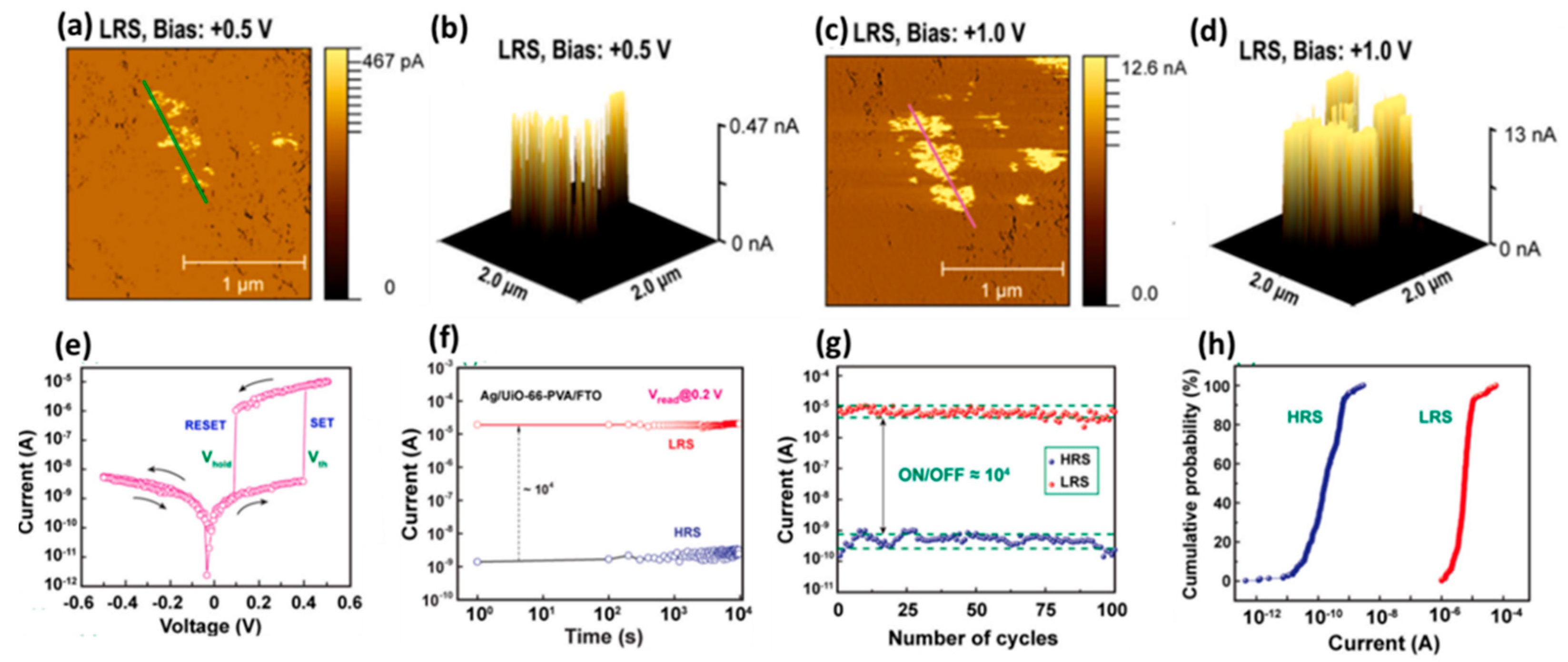
| Ag/UiO-66@PVA/FTO | unipolar | 0.37/0.07 | ~104 | 104 | 5 × 10² | [48] |
| Ag/FJU-23-H2O/Ag ** | bipolar | 0.2/−0.5 | 105 | 104 | 100 | [49] |
| Ti/(SiO2/Si)/Pt/RSMOF-1 | bipolar | ±7.5/∓1.5 | ∼30 | >6000 | 50 | [50] |
| ITO/POMOF/Ag | bipolar | 1.77/−3.42 | 102 | - | 100 | [51] |
| Al/Zn-TCPP nanosheets @PVPy/ITO | bipolar | −0.5/2.4 | 103 | 104 | 103 | [52] |
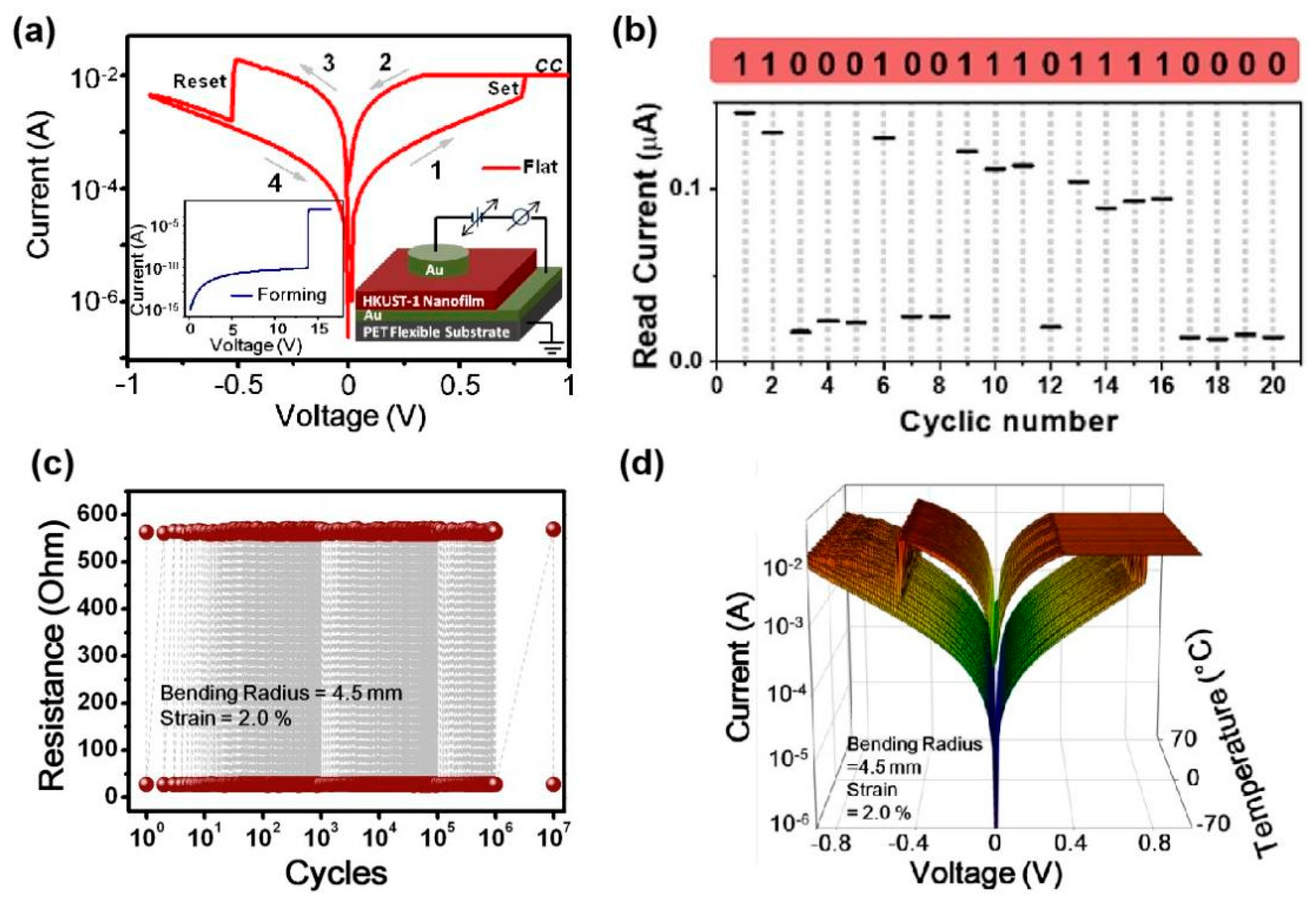
| Au/HKUST-1/Au/PET | bipolar | 0.76/−0.48 | 18.5 | 104 | 107 | [53] |
| Ag/MIL-53/GaInSn@PDMS | bipolar | −1.2/0.3 | 200 | >105 | 200 | [54] |
| (PET/Ti/)Au/ZIF-8/Al | bipolar | −1.9/~1.5 | ~104 | 4000 | - | [55] |
| (PET)/rGO/MoS2@ZIF-8/rGO | WORM | - | 7.0 × 10⁴ | 1500 | - | [56] |
Publisher’s Note: MDPI stays neutral with regard to jurisdictional claims in published maps and institutional affiliations. |
© 2022 by the authors. Licensee MDPI, Basel, Switzerland. This article is an open access article distributed under the terms and conditions of the Creative Commons Attribution (CC BY) license (https://creativecommons.org/licenses/by/4.0/).
Share and Cite
Shu, F.; Chen, X.; Yu, Z.; Gao, P.; Liu, G. Metal–Organic Frameworks–Based Memristors: Materials, Devices, and Applications. Molecules 2022, 27, 8888. https://doi.org/10.3390/molecules27248888
Shu F, Chen X, Yu Z, Gao P, Liu G. Metal–Organic Frameworks–Based Memristors: Materials, Devices, and Applications. Molecules. 2022; 27(24):8888. https://doi.org/10.3390/molecules27248888
Chicago/Turabian StyleShu, Fan, Xinhui Chen, Zhe Yu, Pingqi Gao, and Gang Liu. 2022. "Metal–Organic Frameworks–Based Memristors: Materials, Devices, and Applications" Molecules 27, no. 24: 8888. https://doi.org/10.3390/molecules27248888