
Multi-Physics Fields Simulations and Optimization of Solder Joints in Advanced Electronic Packaging


Abstract
:1. Introduction
2. Numerical Model
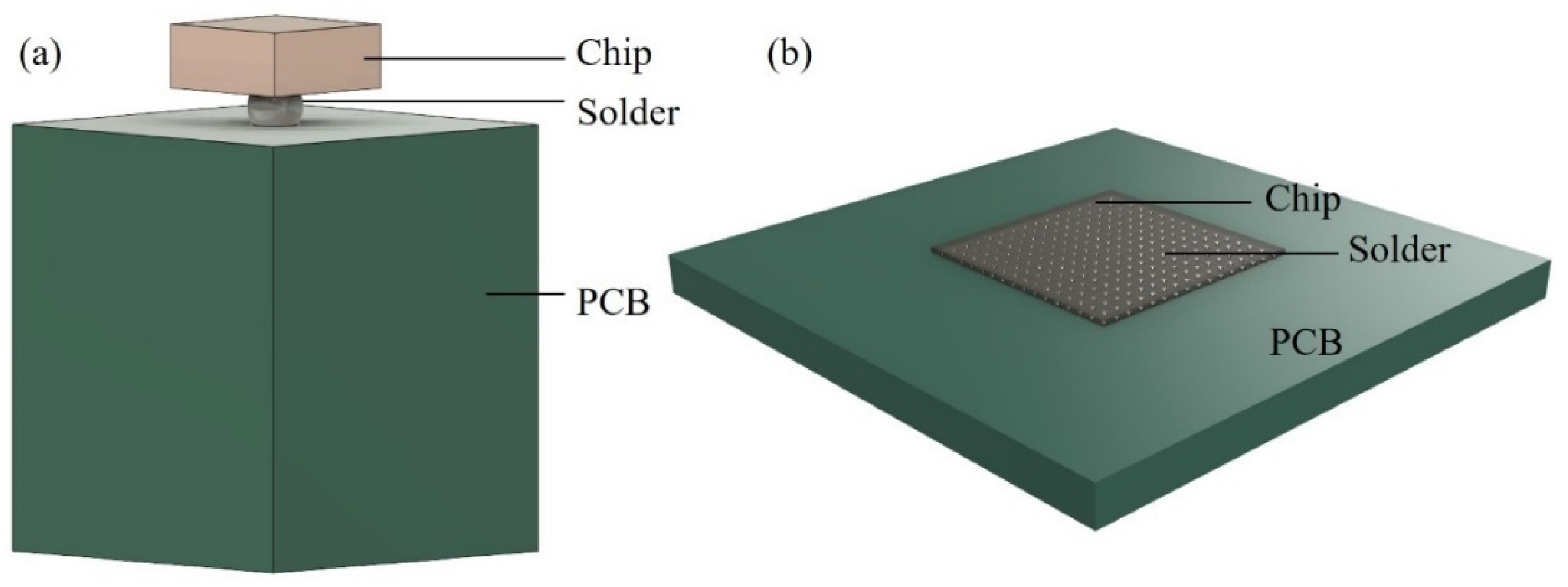
2.1. Physical Model
2.2. Governing Equation
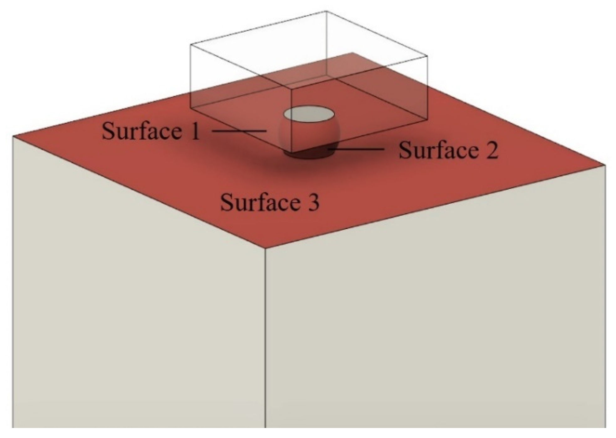
2.3. Boundary Condition
2.4. Coupling of CFD Modules and Structural Model
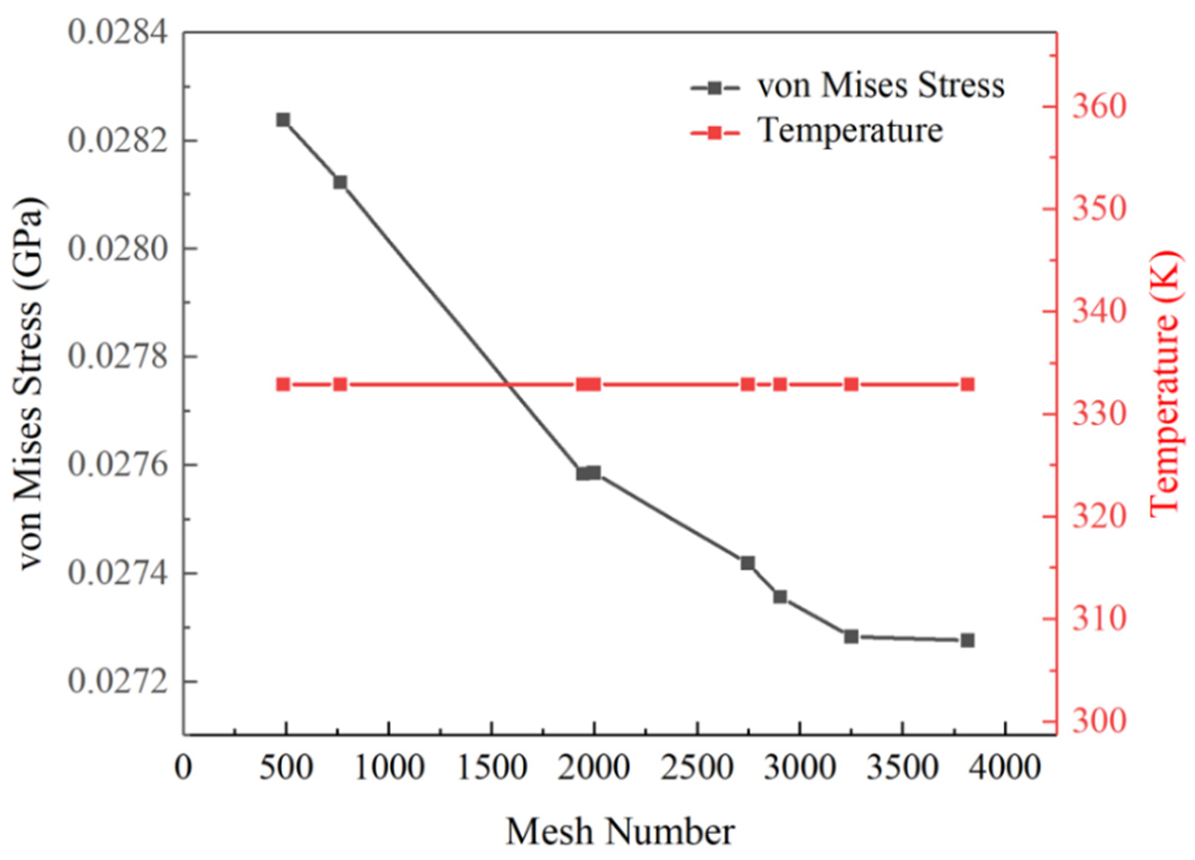
2.5. Model Validation
3. Results and Discussion
3.1. Ball-Grid Array
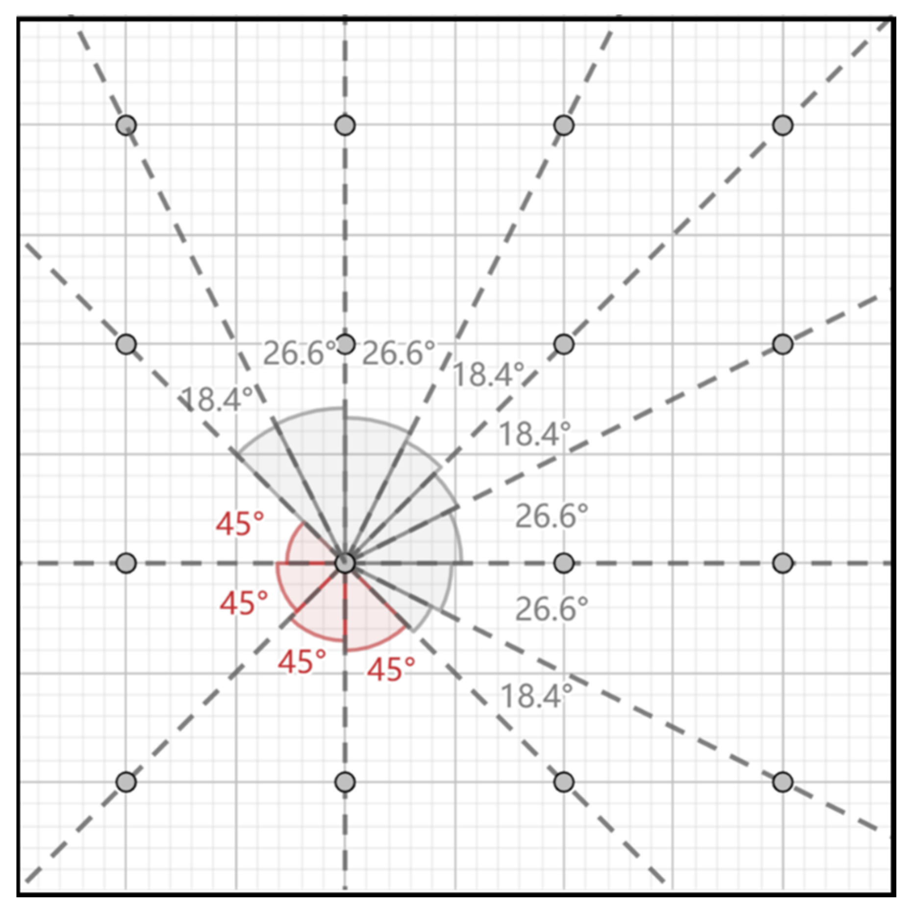
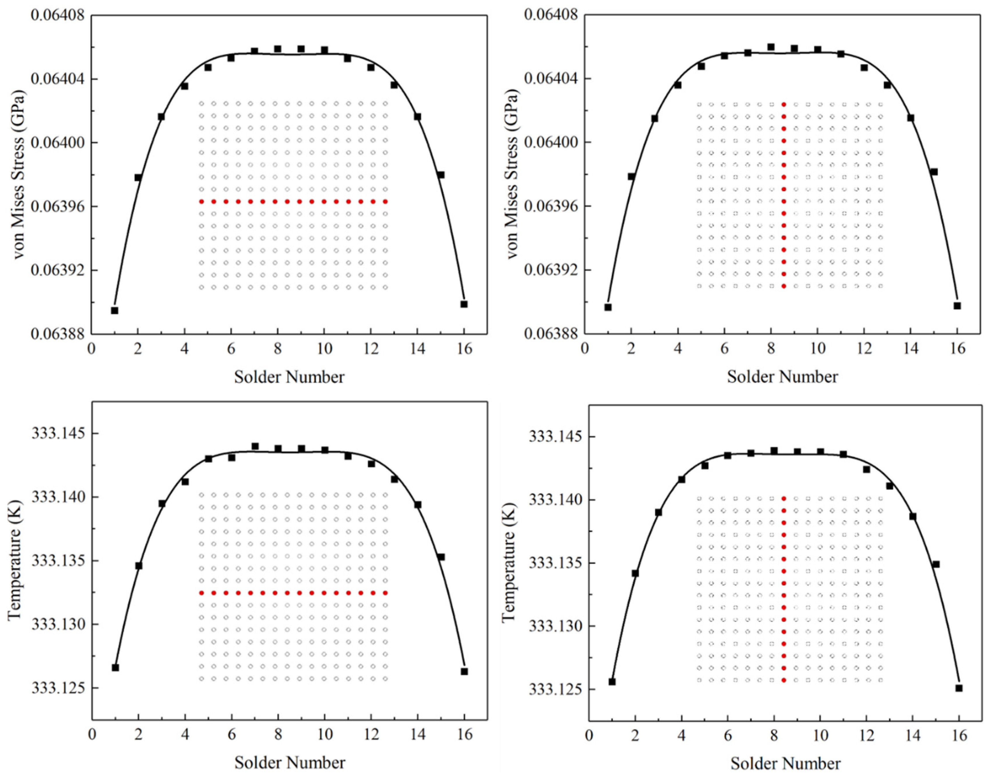
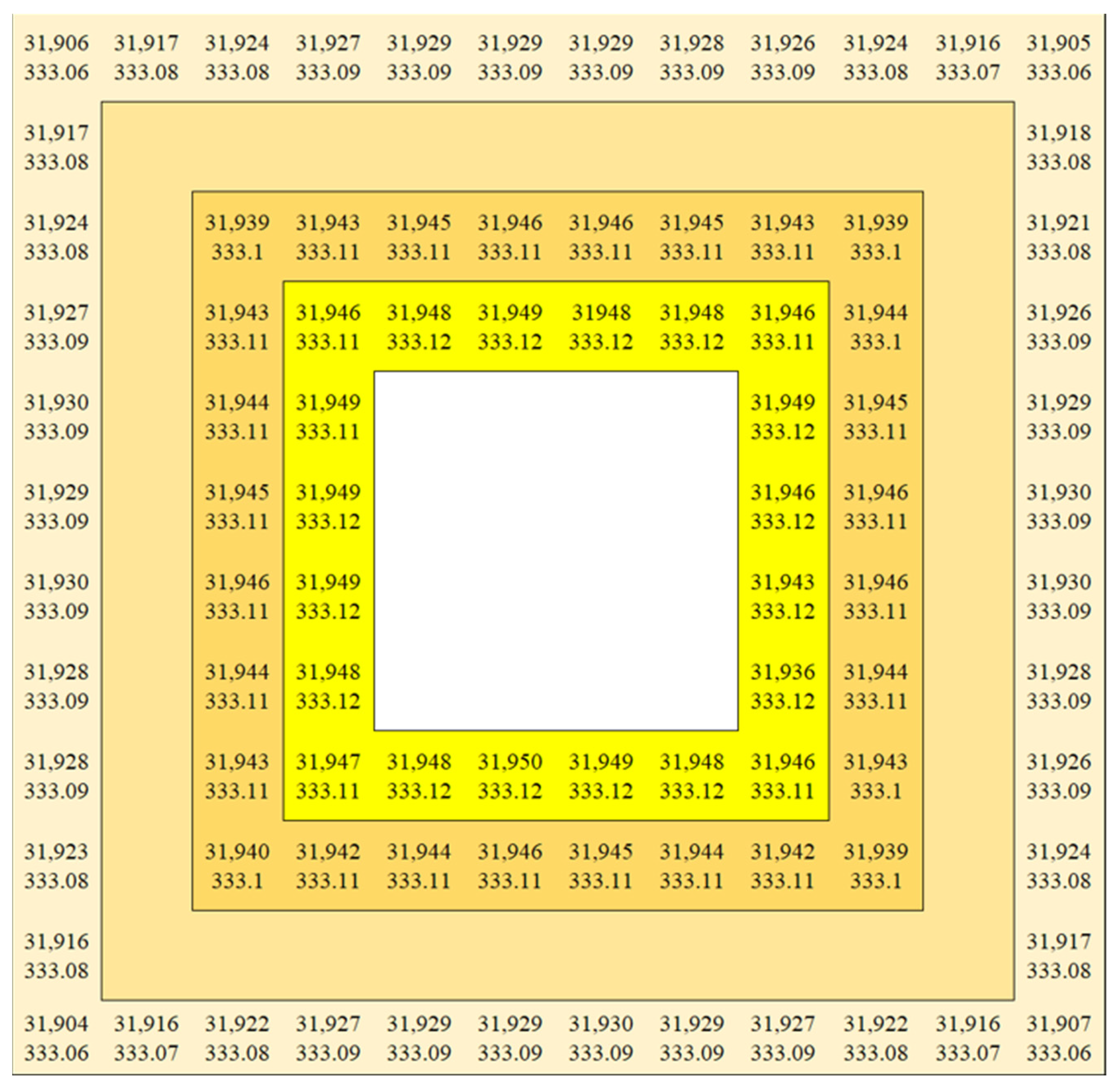
3.1.1. General Distribution Trend
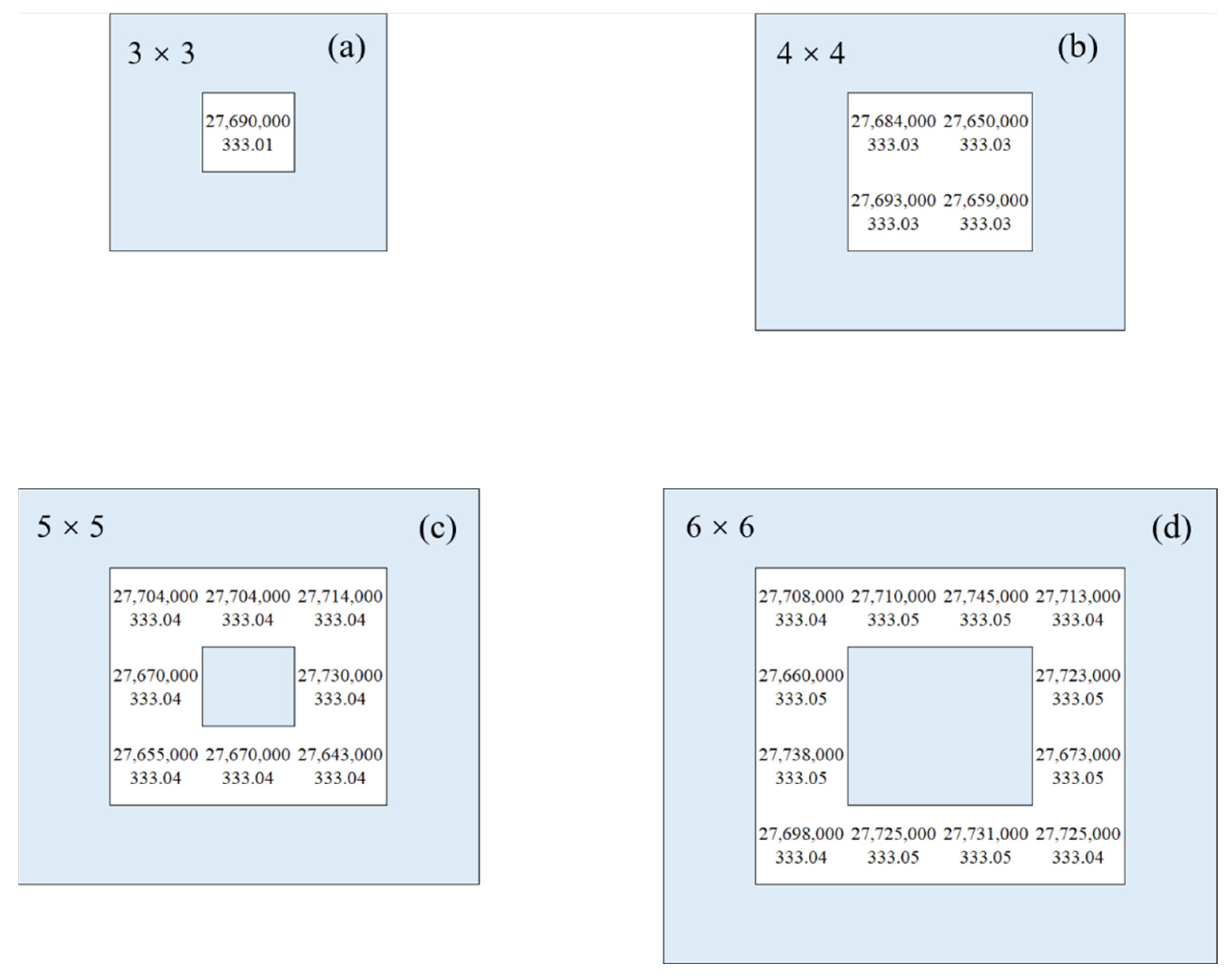
3.1.2. Open Angle Theory Validation
3.2. Single Solder Joint
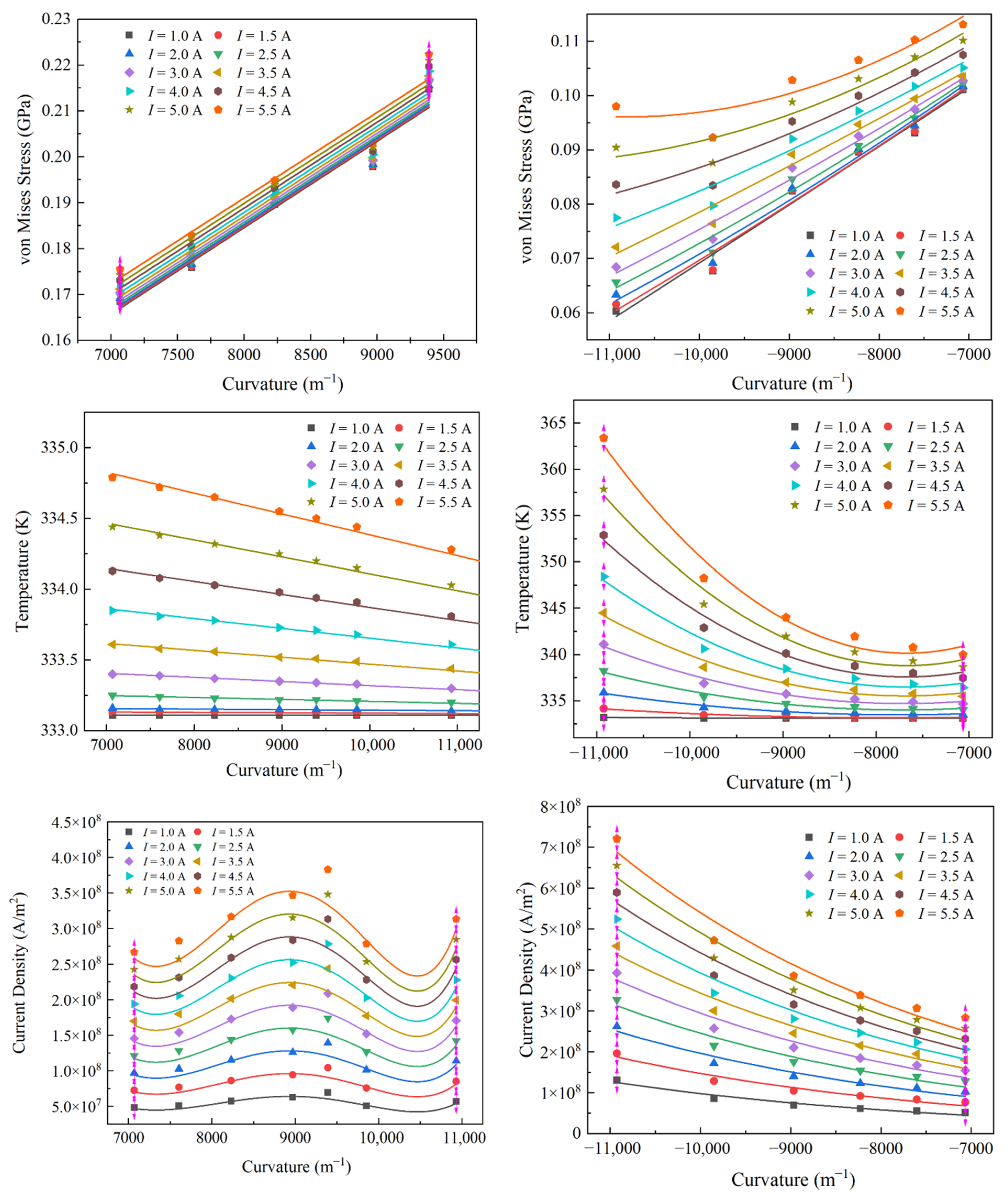
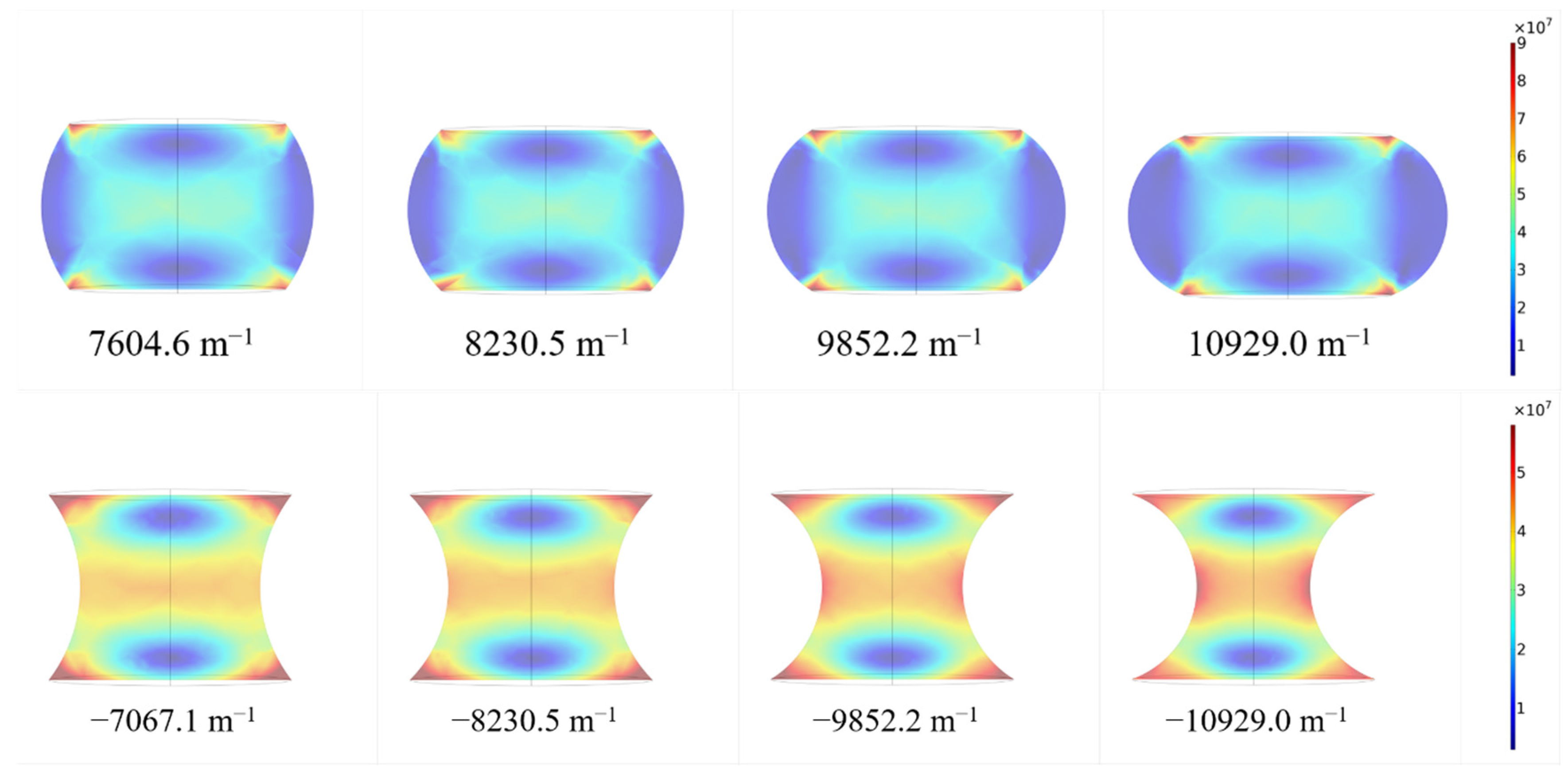
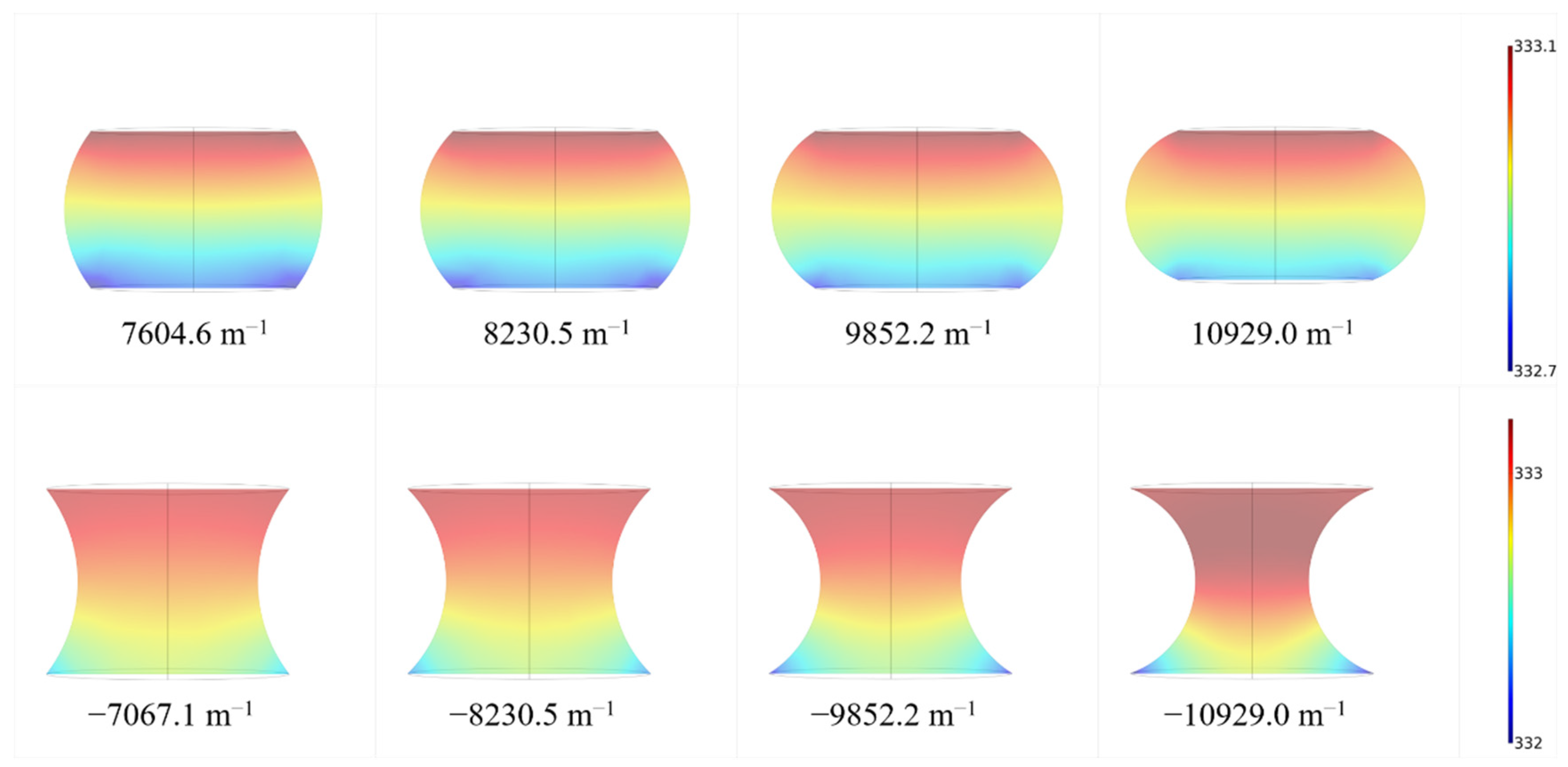
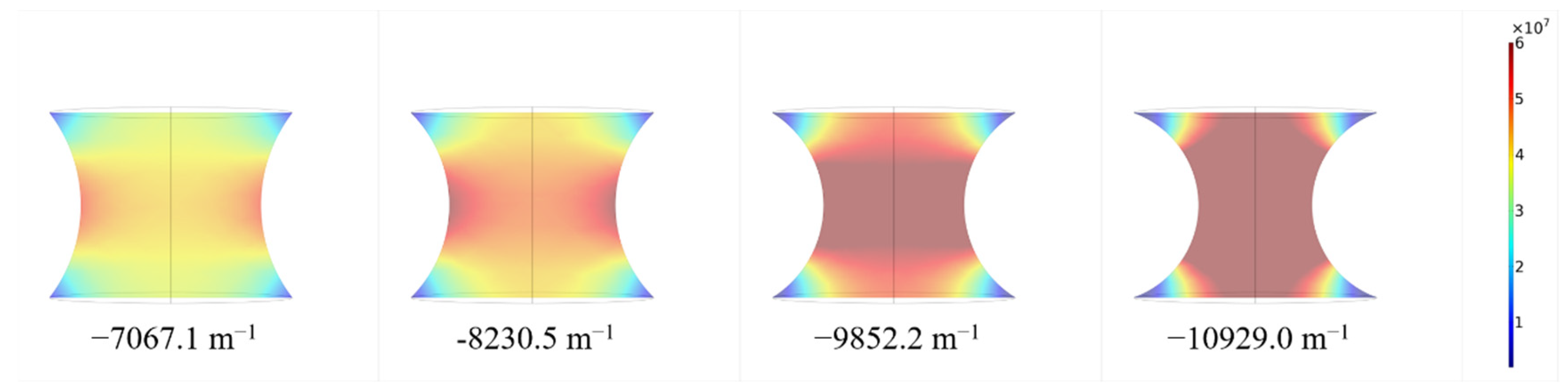
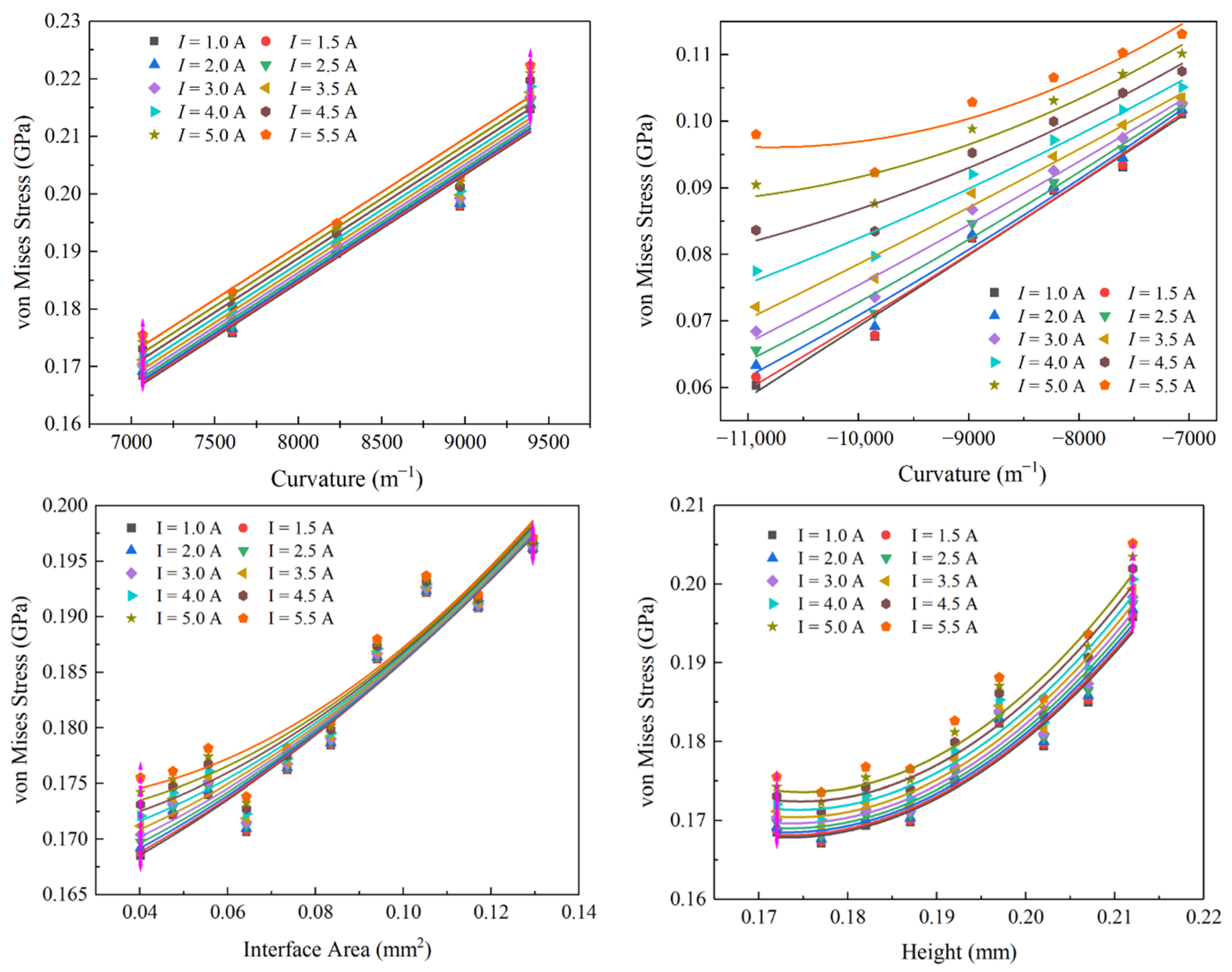
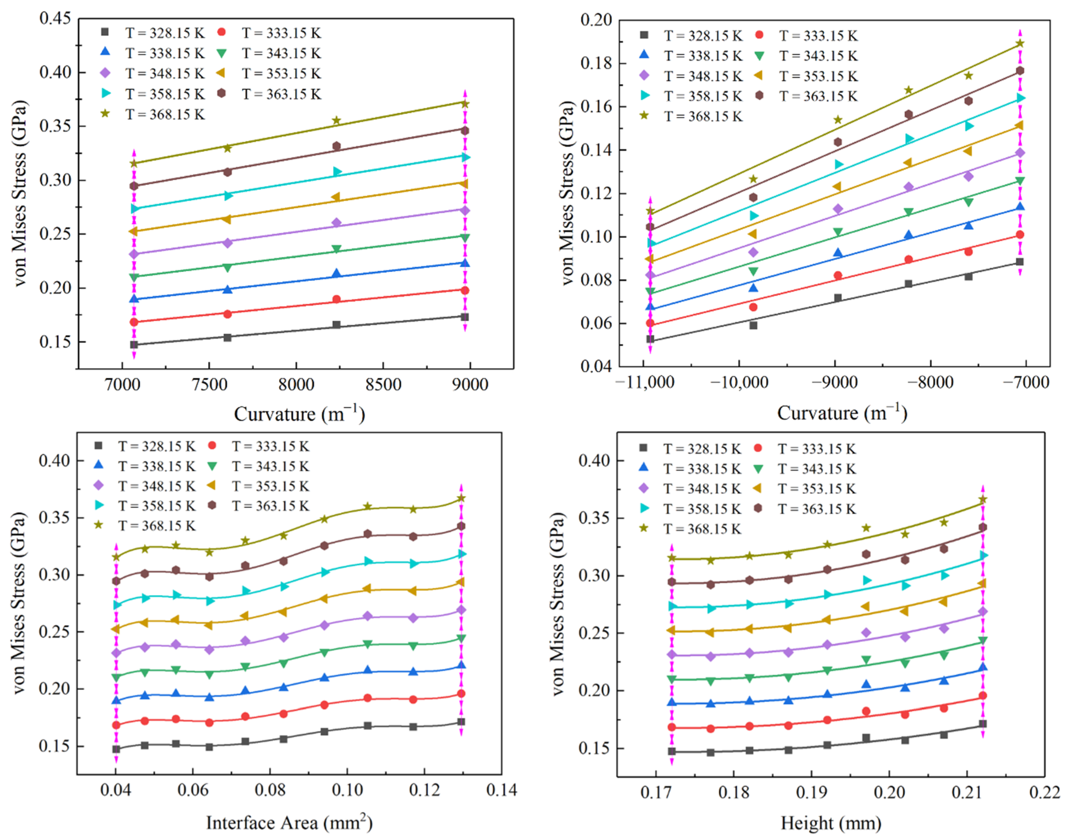
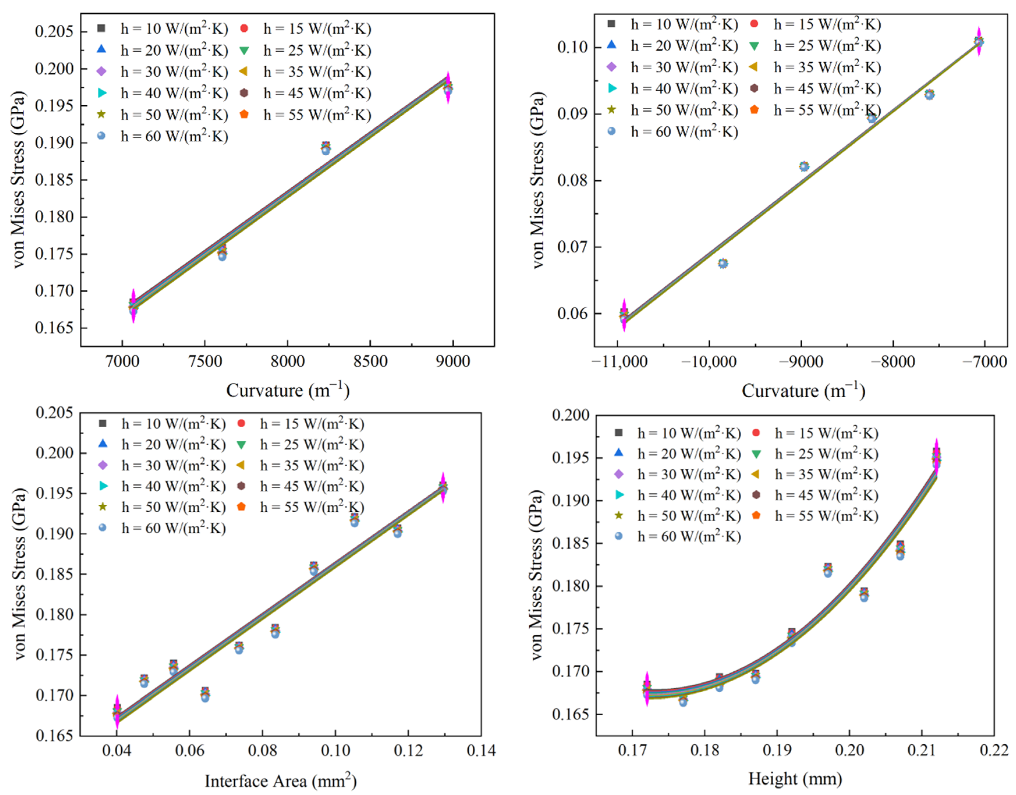
3.2.1. Geometric Shape—Curvature
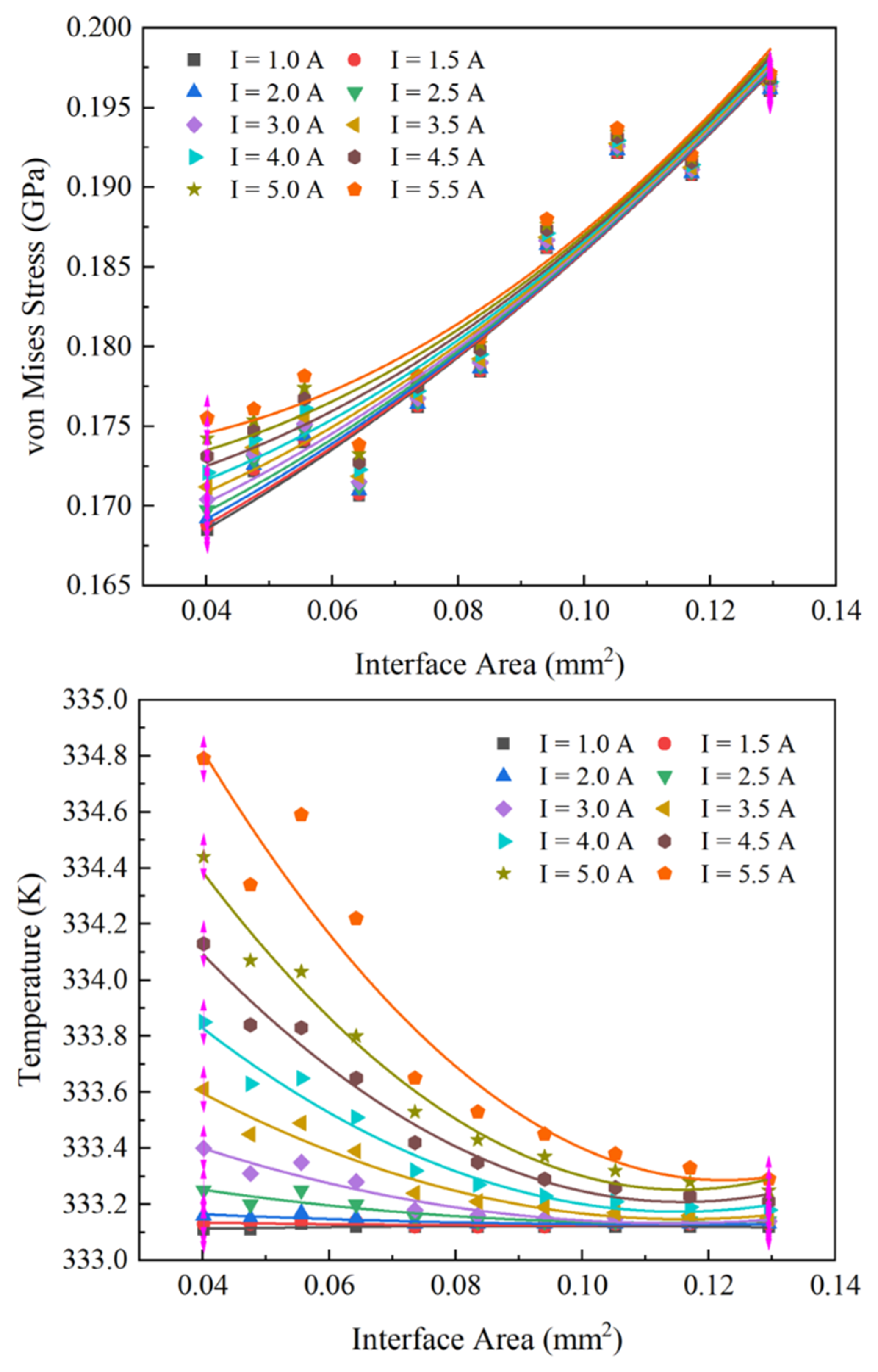
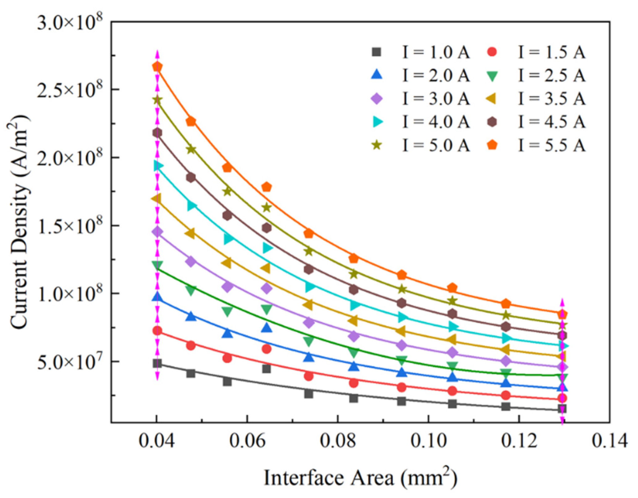
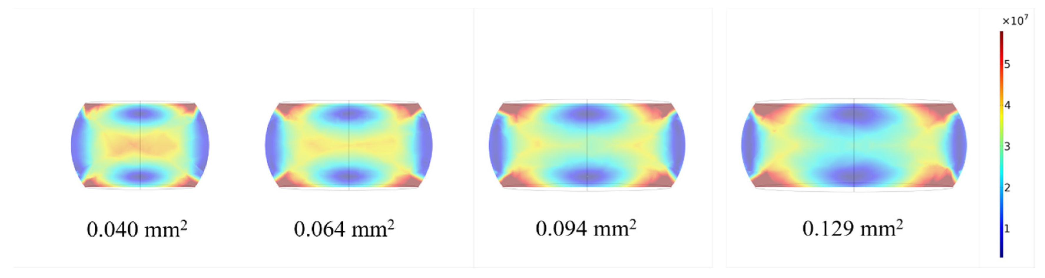
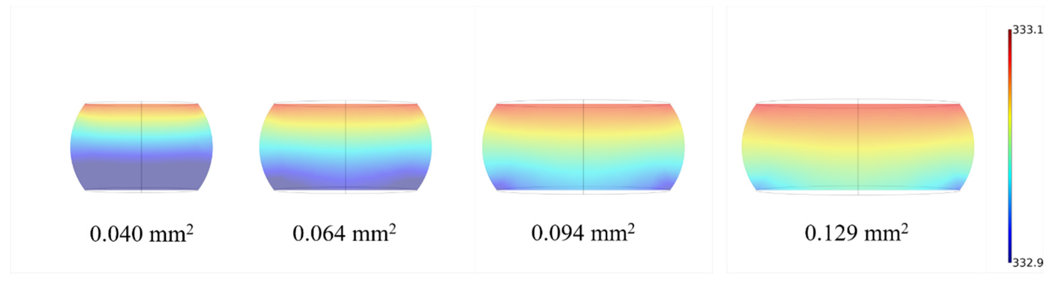
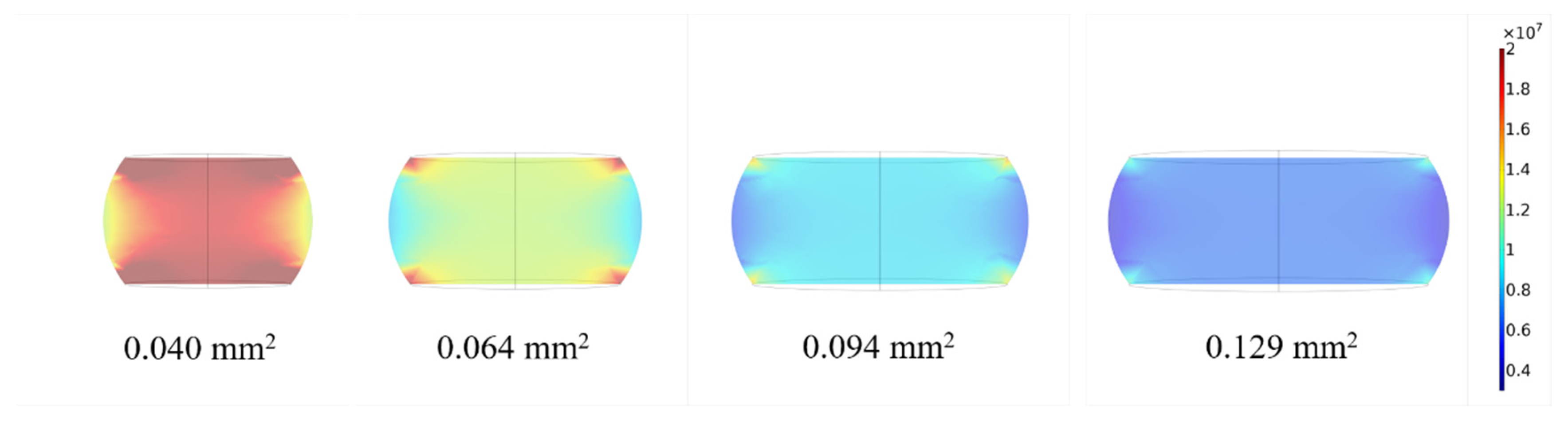
3.2.2. Geometric Shape—Interface Area
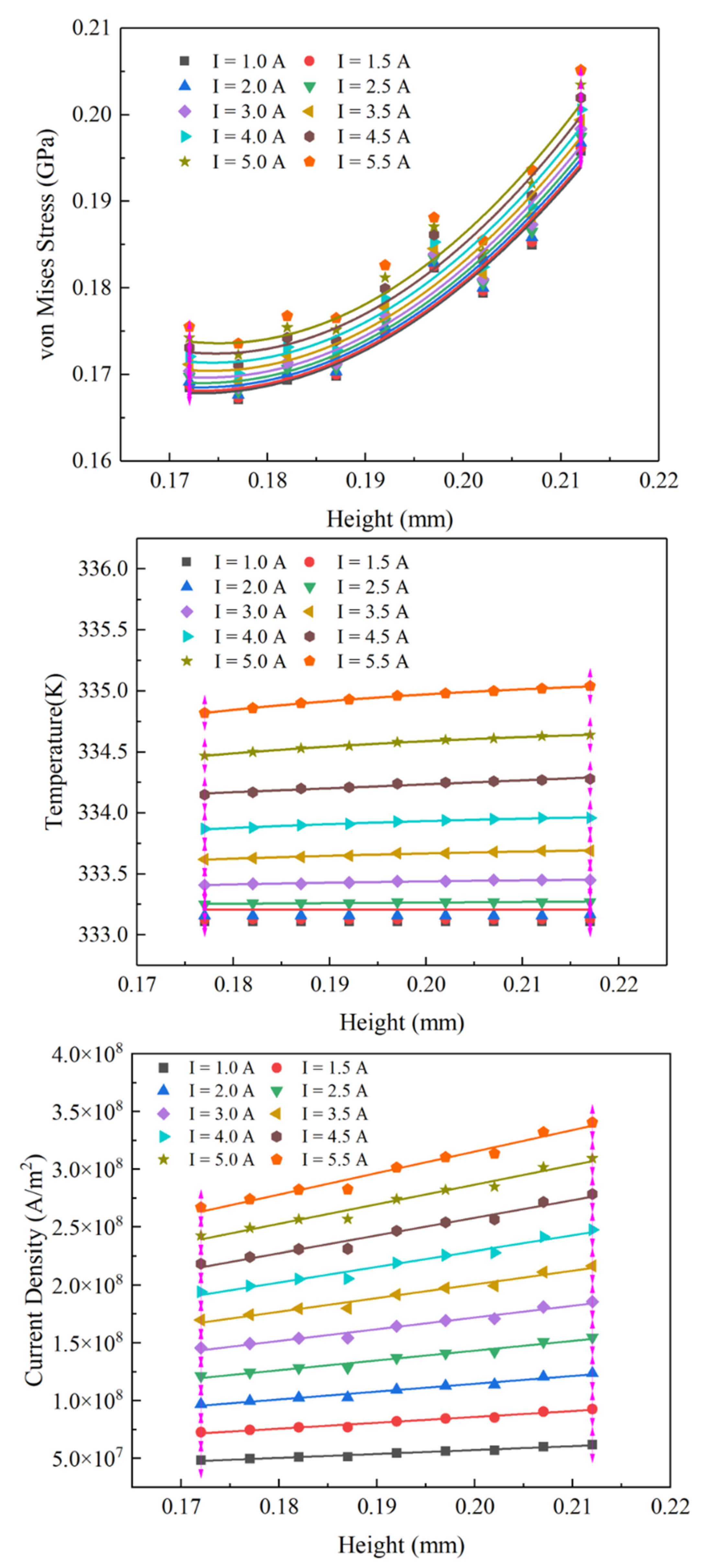
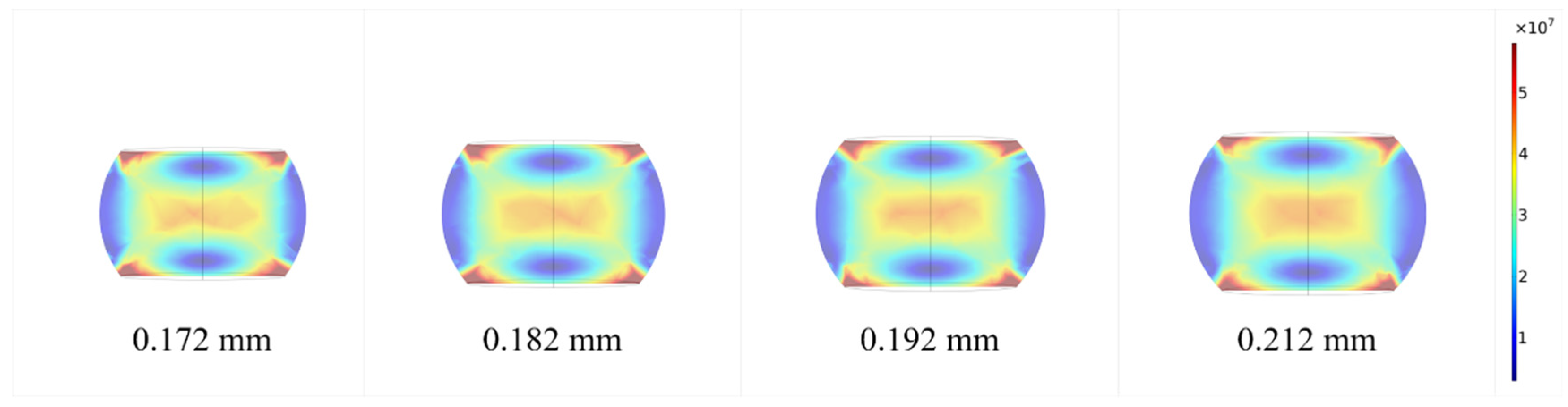
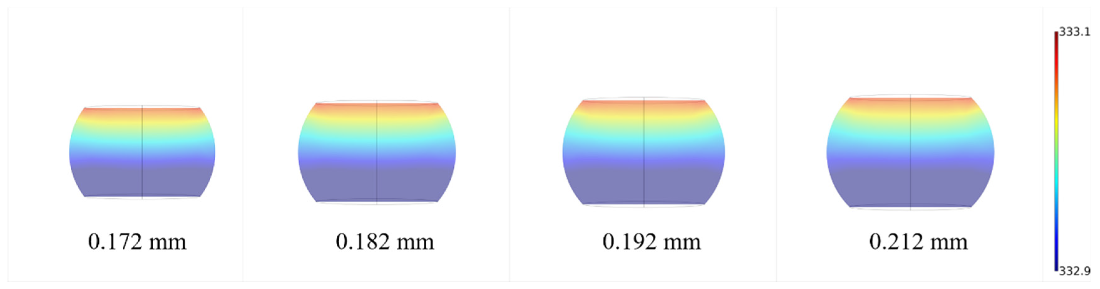
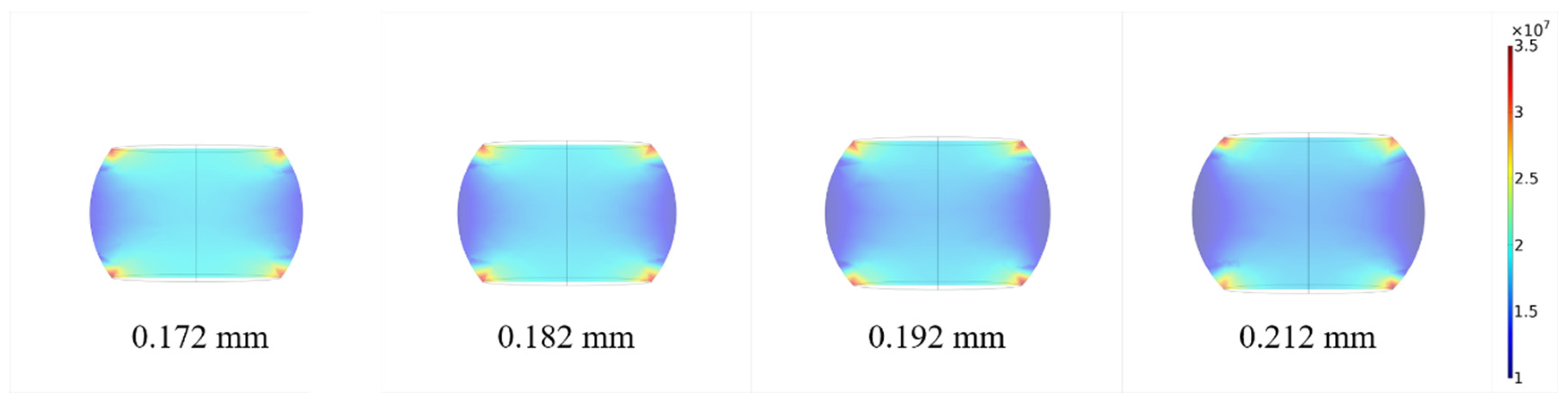
3.2.3. Geometric Shape—Height
3.2.4. Comparison of Impact
3.3. Working Condition
4. Conclusions
Author Contributions
Funding
Institutional Review Board Statement
Informed Consent Statement
Data Availability Statement
Acknowledgments
Conflicts of Interest
References
- Aryan, P.; Sampath, S.; Sohn, H. An overview of non-destructive testing methods for integrated circuit packaging inspection. Sensors 2018, 18, 1981. [Google Scholar] [CrossRef] [PubMed] [Green Version]
- Longford, A. Chip packaging challenges… a roadmap based overview. Microelectron. Int. 2005, 22, 17–20. [Google Scholar] [CrossRef]
- Cognetti, C. The impact of semiconductor packaging technologies on system integration an overview. In Proceedings of the 2009 Proceedings of the European Solid State Device Research Conference, Athens, Greece, 14–18 September 2009; pp. 24–28. [Google Scholar]
- Garrou, P. Wafer level chip scale packaging (WL-CSP): An overview. IEEE Trans. Adv. Packag. 2000, 23, 198–205. [Google Scholar] [CrossRef]
- Ryu, C.; Hsu, J.; Mendoza, L.; Capuz, A.; Caguiat, J.; Sy, H.; Lathrop, R. Novel approaches to current bga packaging challenges. In Proceedings of the 2008 10th Electronics Packaging Technology Conference, Singapore, 9–12 December 2008; pp. 1258–1263. [Google Scholar]
- Datta, M. Manufacturing processes for fabrication of flip-chip micro-bumps used in microelectronic packaging: An overview. J. Micromanufacturing 2020, 3, 69–83. [Google Scholar] [CrossRef]
- Chen, C.; Hsiao, H.Y.; Chang, Y.W.; Ouyang, F.; Tu, K.N. Thermomigration in solder joints. Mater. Sci. Eng. R Rep. 2012, 73, 85–100. [Google Scholar] [CrossRef]
- Frear, D.R.; Grivas, D.; Morris, J.W. Thermal fatigue in solder joints. JOM 1988, 40, 18–22. [Google Scholar] [CrossRef]
- Adams, P.J. Thermal Fatigue of Solder Joints in Micro-Electronic Devices. Ph.D. Thesis, Massachusetts Institute of Technology, Cambridge, MA, USA, 1986. [Google Scholar]
- Ye, H.; Basaran, C.; Hopkins, D.C.; Frear, D.; Lin, J.K. Damage mechanics of microelectronics solder joints under high current densities. In Proceedings of the 2004 Proceedings, 54th Electronic Components and Technology Conference (IEEE Cat. No.04CH37546), Las Vegas, NV, USA, 4 June 2004; Volume 1, pp. 988–997. [Google Scholar]
- Zuo, Y.; Ma, L.; Liu, S.; Wang, T.; Guo, F.; Wang, X. The coupling effects of thermal cycling and high current density on Sn58Bi solder joints. J. Mater. Sci. 2013, 48, 2318–2325. [Google Scholar] [CrossRef]
- Di Maio, D.; Murdoch, C.; Thomas, O.; Hunt, C. The degradation of solder joints under high current density and low-cycle fatigue. In Proceedings of the 2010 11th International Thermal, Mechanical & Multi-Physics Simulation, and Experiments in Microelectronics and Microsystems (EuroSimE), Bordeaux, France, 26–28 April 2010; pp. 1–6. [Google Scholar]
- Ye, H.; Basaran, C.; Hopkins, D.C. Pb phase coarsening in eutectic Pb/Sn flip chip solder joints under electric current stressing. Int. J. Solids Struct. 2004, 41, 2743–2755. [Google Scholar] [CrossRef]
- Subrahmanyan, R.; Wilcox, J.R.; Li, C.Y. A damage integral approach to thermal fatigue of solder joints. IEEE Trans. Compon. Hybrids Manuf. Technol. 1989, 12, 480–491. [Google Scholar] [CrossRef]
- Liu, C.M.; Chiang, K.N. Solder shape design and thermal stress/strain analysis of flip chip packaging using hybrid method. In Proceedings of the International Symposium on Electronic Materials and Packaging (EMAP2000) (Cat. No. 00EX458), Hong Kong, China, 30 November–2 December 2000; pp. 44–50. [Google Scholar]
- Peng, C.T.; Liu, C.M.; Lin, J.C.; Cheng, H.C.; Chiang, K.N. Reliability analysis and design for the fine-pitch flip chip BGA packaging. IEEE Trans. Compon. Packag. Technol. 2004, 27, 684–693. [Google Scholar] [CrossRef]
- Wu, L.; Han, X.; Shao, C.; Yao, F.; Yang, W. Thermal fatigue modelling and simulation of flip chip component solder joints under cyclic thermal loading. Energies 2019, 12, 2391. [Google Scholar] [CrossRef] [Green Version]
- Tang, X.Q.; Zhao, S.J.; Huang, C.Y.; Lu, L.K. Thermal stress-strain simulation analysis of BGA solder joint reflow soldering process. In Proceedings of the 2018 19th International Conference on Electronic Packaging Technology (ICEPT), Shanghai, China, 8–11 August 2018; pp. 981–986. [Google Scholar]
- Lau, C.S.; Abdullah, M.Z.; Ani, F.C. Computational fluid dynamic and thermal analysis for BGA assembly during forced convection reflow soldering process. Solder. Surf. Mt. Technol. 2012, 24, 77–91. [Google Scholar] [CrossRef]
- Depiver, J.A.; Mallik, S.; Amalu, E.H. Effective solder for improved thermo-mechanical reliability of solder joints in a ball grid array (BGA) soldered on printed circuit board (PCB). J. Electron. Mater. 2021, 50, 263–282. [Google Scholar] [CrossRef]
- Fan, X.; Pei, M.; Bhatti, P.K. Effect of finite element modeling techniques on solder joint fatigue life prediction of flip-chip BGA packages. In Proceedings of the 56th Electronic Components and Technology Conference 2006, San Diego, CA, USA, 30 May–2 June 2006; p. 9. [Google Scholar]
- Edwards, D.A.; Shapiro, M.; Brenner, H.; Shapira, M. Dispersion of inert solutes in spatially periodic, two-dimensional model porous media. Transp. Porous Media 1991, 6, 337–358. [Google Scholar] [CrossRef]
- Yi, S.; Sze, K.Y. Finite element analysis of moisture distribution and hygrothermal stresses in TSOP IC packages. Finite Elem. Anal. Des. 1998, 30, 65–79. [Google Scholar] [CrossRef]
- Wang, J.; He, P.; Xiao, F. The effect of residual stress on the flexing strength of PCB assembly. In Proceedings of the Sixth IEEE CPMT Conference on High Density Microsystem Design and Packaging and Component Failure Analysis (HDP’04), Shanghai, China, 3 July 2004; pp. 146–150. [Google Scholar]
- Puibasset, J. Elastic Compliance and Stiffness Matrix of the FCC Lennard-Jones Thin Films: Influence of Thickness and Temperature. J. Phys. Chem. C 2019, 123, 15027–15037. [Google Scholar] [CrossRef] [Green Version]
- Kosky, P.; Balmer, R.; Keat, W.; Wise, G. Exploring Engineering: An Introduction to Engineering and Design; Academic Press: Cambridge, MA, USA, 2015. [Google Scholar]
- Awbi, H.B. Calculation of convective heat transfer coefficients of room surfaces for natural convection. Energy Build. 1998, 28, 219–227. [Google Scholar] [CrossRef]
- Krishnamoorthi, S.; Chong, D.Y.; Sun, A.Y. Thermal management and characterization of flip chip BGA packages. In Proceedings of the 6th Electronics Packaging Technology Conference (EPTC 2004) (IEEE Cat. No. 04EX971), Singapore, 8–10 December 2004; pp. 53–59. [Google Scholar]


| Material | Sn62Pb36Ag2 | Silicon | FR-4 |
|---|---|---|---|
| σ (S/m) | 5,714,285 | 10−5 | 10−5 |
| ε (a) | 1 | 1 | 1 |
| E (Pa) | 2.6 × 10¹⁰ | 1.31 × 10¹¹ | 2.4 × 10¹⁰ |
| α (1/K) | 2.45 × 10⁻⁵ | 2.6 × 10⁻⁶ | 1.4 × 10⁻⁵ |
| ν (1) | 0.35 | 0.28 | 0.136 |
| k (W/(m·K)) | 36 | 130 | 0.25 |
| cp (j/(kg·K)) | 400 | 871.75 | 1100 |
| K (Pa) | 5.5 × 10¹⁰ | 9.8 × 10¹¹ | 3.8 × 10⁹ |
| ρ (kg/m3) | 7000 | 2329 | 1850 |
| ρ0 (Ω·m) | 1.4 × 10⁻⁷ | 2.3 × 10³ | 5 × 10⁹ |
Publisher’s Note: MDPI stays neutral with regard to jurisdictional claims in published maps and institutional affiliations. |
© 2022 by the authors. Licensee MDPI, Basel, Switzerland. This article is an open access article distributed under the terms and conditions of the Creative Commons Attribution (CC BY) license (https://creativecommons.org/licenses/by/4.0/).
Share and Cite
Yu, B.; Gao, Y. Multi-Physics Fields Simulations and Optimization of Solder Joints in Advanced Electronic Packaging. Chips 2022, 1, 191-209. https://doi.org/10.3390/chips1030013
Yu B, Gao Y. Multi-Physics Fields Simulations and Optimization of Solder Joints in Advanced Electronic Packaging. Chips. 2022; 1(3):191-209. https://doi.org/10.3390/chips1030013
Chicago/Turabian StyleYu, Boyan, and Yisai Gao. 2022. "Multi-Physics Fields Simulations and Optimization of Solder Joints in Advanced Electronic Packaging" Chips 1, no. 3: 191-209. https://doi.org/10.3390/chips1030013