Article

Design Guideline for a Cantilever-Type MEMS Switch with High Contact Force

Valiev Institute of Physics and Technology, Russian Academy of Sciences, Yaroslavl Branch, Universitetskaya 21, 150007 Yaroslavl, Russia
*
Author to whom correspondence should be addressed.
Micro 2024, 4(1), 1-13; https://doi.org/10.3390/micro4010001
Submission received: 7 November 2023 / Revised: 5 December 2023 / Accepted: 18 December 2023 / Published: 20 December 2023

Abstract

:
Micromechanical switches are of significant interest for advanced radio frequency and microwave systems, but their practical implementation is limited by low reliability. Electrodes of a microscopic size develop weak contact force that leads to high and unstable contact resistance. The force is typically increased by using a sophisticated switch design with extended lateral dimensions, although a simple and compact cantilever is more preferable. The paper describes for the first time a comprehensive approach to enhance the force of an electrostatically actuated switch. The strategy is applied to a miniature device based on a 50 µm long cantilever. The contact force is increased from 10 to 112 µN, making the switch strong enough to achieve low and stable contact resistance. The restoring force is also enhanced in order to ensure reliable de-actuation. The growth of forces is accompanied by a reduction in the pull-in voltage. Connecting several cantilevers in parallel and manipulating the number and position of contact bumps additionally improves the force and mechanical stability of the switch. An optimal design contains a triple cantilever with two bumps. It provides 50% higher force per contact compared to the single-cantilever switch at the same pull-in voltage and keeps the advantages of a miniature device. The proposed design strategy may be used for building reliable MEMS switches.

1. Introduction

In recent decades, microelectromechanical system (MEMS) switches have been actively considered as promising electronic components for radio frequency and microwave systems [1]. Small size, low insertion loss, high isolation and low power consumption make them attractive for use in 5G communication networks [2,3,4], adaptive antennas [5,6,7,8], aeronautical and space equipment [9,10]. MEMS switches utilize various actuation principles including electromagnetic, piezoelectric, thermal, and inertial, but electrostatic actuation is the most popular driving mechanism (see the review papers [11,12]). A conventional MEMS switch consists of a cantilever suspended above driving and signal electrodes. Applying voltage to the driving electrode creates an electrostatic force that bends the cantilever and brings it in contact with the signal electrode. When the voltage is turned off, the cantilever goes back to initial position under the elastic force. Electrostatic MEMS switches are fabricated by microelectronic techniques and can be easily integrated with CMOS circuits [13,14]. Combining multiple switches on a single chip allows the fabrication of reconfigurable devices such as phase shifters [15,16,17], filters [18,19], attenuators [20,21,22], and amplifiers [23,24].
Along with the driving principle, MEMS switches are classified by the type of contact. Resistive switches provide metal-to-metal contact, while capacitive devices realize metal–insulator–metal contact. Resistive switches are preferable for many applications due to a wide bandwidth from DC to RF frequencies. However, despite three decades of research, they still suffer from a lack of reliability [25,26]. A principal problem is the small contact force developed by the micron-sized beam. MEMS switches typically operate in the micronewton range. This force is several orders of magnitude lower compared to millinewtons delivered by macroscopic electromechanical relays [1]. Weak force makes contacting surfaces sensitive to contamination and damage, which leads to instability and a rapid increase in the contact resistance [27,28].
The problem is well understood by the MEMS community. The operation of microscopic contacts is thoroughly investigated using indenters [29,30,31], scanning probe microscopes [32,33], and homemade facilities [34,35,36,37,38]. It is demonstrated that the contact resistance rapidly decreases with increasing the force and then reaches saturation. A low and stable resistance is achieved when the force exceeds 100 µN. This value is considered as a necessary threshold for the switch reliability [1]. However, such a force is hardly achievable in the conventional design. To solve the problem, the cantilever is replaced by circular frames [39,40,41], crab-leg structures [42,43], and extended membranes [44,45]. They produce strong force due to the large lateral size of several hundred microns. But wide dimensions make the switch sensitive to mechanical stress, because even a small stress gradient leads to a significant variation of the gap between the electrodes. In addition, increasing the size reduces switching speed, increases parasitic capacitance, and degrades RF performance. The sophisticated design of the switch complicates integration into a coplanar transmission line.
The cantilever-based switch is more convenient. Its simple design allows the realization of both series and shunt configurations and building a multi-component device like a phase shifter. A miniature cantilever ensures stress robustness and short switching time [46]. However, the cantilever-based devices typically demonstrate low contact force of several tens of micronewtons [15,16,46,47,48]. This paper describes a comprehensive strategy for increasing the contact force of the conventional MEMS switch without enlargement of its lateral size. A tiny cantilever with the length of 50 µm is considered. Vertical dimensions of the switch are adjusted to raise the force above 100 µN. The restoring force is also increased in order to protect the device from stiction. For the first time, we propose the parallel connection of several cantilevers and choosing the number and position of contact bumps. This approach additionally enhances the forces and mechanical stability of the cantilever.

2. Materials and Methods

The importance of the contact force for a resistive switch is described by a contact model of the cantilever with the signal electrode. The contact is formed by surface asperities and can be presented as a set of spots with different area; see Figure 1. The total contact area is characterized by the effective radius reff. The contact resistance Rc is determined as follows [27]:
R c = ρ 2 r e f f ,
where ρ is the resistivity of contacting materials. If the contact force is weak (below 200 µN [28]), the materials undergo elastic deformation, and reff is written as:
r e f f = 3 F c δ 4 E e f f 3 ,
where Fc is the contact force, δ is the asperity peak radius of curvature, and Eeff is the effective Hertzian modulus derived from:
1 E e f f = 1 υ 1 2 E 1 + 1 υ 2 2 E 2 ,
where E1, E2 and υ1, υ2 are the Young’s modules and Poisson’s coefficients of the materials one and two. When the force exceeds 200 µN, plastic deformation takes place, and the effective radius is determined as:
r e f f = F c π H ,
where H is the Meyer hardness of the softer material.
According to Equations (1), (2) and (4), the contact resistance is determined by the material properties and contact force. The contacts are typically made of noble metals due to their high conductivity and chemical inertness [1]. Therefore, the choice of electrical and elastic properties is limited, while Fc depends on the switch design and can vary over a wide range. For the elastic and plastic regimes, Rc is inversely proportional to Fc1/3 and Fc1/2, respectively. Thus, one has to increase the force in order to reduce the resistance. In addition, a large Fc helps to break contaminating films and enhances the stability of Rc from cycle to cycle [35]. Experimental data suggest the minimum required value of 100 µN per contact [29,30,31,33,38].
It is worth noting that increasing Fc expands the contact area and leads to higher adhesion. Therefore, the growth of the contact force must be accompanied by an increment in the restoring force Fr in order to ensure de-actuation. It is generally accepted that Fr of more than one-third of Fc is necessary for a stable restoration action [44]. This relation has to be considered when the switch is designed.
Here, we propose a strategy to increase the contact and restoring forces of the compact cantilever-based switch. This strategy is applied to the device shown schematically in Figure 2. A movable electrode is an aluminum cantilever with the length l = 50 µm and width w = 10 µm at the fixed end. The free part is widened to we = 20 µm. The driving electrode surrounds the signal one and provides the overlap area A = 430 µm2 with the cantilever. The widening and surrounding are commonly used to expand the electrostatic field area without significant increase in the switch size [46,49,50]. The cantilever has the thickness t = 2.0 µm. A contact bump with the height h = 0.5 µm is located on its bottom surface. The air gap between the cantilever and electrodes is g0 = 1.5 µm. A detailed description of the switch is given in [51].
The contact force may be calculated by the finite element method (FEM) simulation, as shown, for example, in [16]. However, this approach requires solving the two-body contact problem, which is a non-trivial and time-consuming task. This shortcoming is especially perceptible when several design parameters are varied. The simple configuration of the switch allows the usage of a straightforward analytical model to calculate the forces. The cantilever exhibits small bending during operation, i.e., l >> g0h. In the bottom position, its profile can be approximated by a straight line, as shown in Figure 3. In this case, the gap between the cantilever and the driving electrode linearly depends on the longitudinal coordinate:
g ( x ) = g 0 b x ,
where the coefficient b is derived as follows:
b = sin α = g 0 h l .
In the middle of the driving electrode, the gap has the following value:
g m i d = g 0 g 0 h l x 2 + x 1 2 ,
where x1 = 25 µm and x2 = 50 µm are the coordinates of the left and right electrode edges. This gap is used to calculate the electrostatic force in the closed state:
F e s = ε ε 0 A V 2 2 g m i d 2 ,
where ε is the dielectric permittivity of the medium (assumed to be air), ε0 is the electric constant, and V is the voltage applied to the driving electrode with respect to the grounded cantilever. Electrostatic switches typically operate at the driving voltage of several tens of volts. At V = 90 V, the electrostatic force is equal to Fes = 28 µN.
The restoring force is determined by Hooke’s law:
F r = k g 0 h ,
where k is the stiffness coefficient of the cantilever. Taking into account the location of the driving electrode, the stiffness takes the form [52]:
k = 2 E w t L 3 1 x 1 / x 2 3 4 x 1 / x 2 3 x 1 / x 2 4 ,
where E = 70 GPa is the Young’s modulus of aluminum. Equation (10) does not consider the widened part of the cantilever, since the deformation and stress are mainly localized near the fixed end [53]. The stiffness coefficient is of 18 N/m, so the cantilever provides Fr = 18 µN.
The contact force is determined by the difference between the electrostatic and elastic forces:
F c = F e s F r .
According to this equation, the switch develops Fc = 10 µN, which is a rather low value. With such a force, Rc is large and varies dramatically from cycle to cycle, as we demonstrated previously [54,55]. Increasing Fc by reducing Fr is limited and raises the tendency to stiction. Another way is to raise Fes by using higher V, but higher voltage increases power consumption and may cause the collapse of the cantilever. Enlarging A is also unacceptable, since the switch loses the advantages of a miniature device. Thus, the force is enhanced by manipulating the vertical dimensions h, g0 and t.
It is worth noting that the contact force of 10 µN is typical for conventional design. Most of the cantilever-type switches develop Fc from 0.6 to 30 µN [15,16,46,47,48]. These devices have various vertical dimensions. There are no specific values that can be considered conventional. For example, a switch with h = 1 μm, g0 = 2.5 μm and t = 2 μm provides the contact force of 18 μN [15]. However, some cantilever-based switches with similar vertical size provide a significantly higher force of 113–301 µN [50,56,57]. They use large cantilevers with the length of 300–485 μm, which suffer from bending under residual mechanical stress, reduce switching speed and increase parasitic capacitance.
Along with the contact and restoring force, an important characteristic is the pull-in voltage Vpull-in, which is calculated using a well-known expression [52]:
V p u l l i n = 8 k 27 ε ε 0 A g 0 3 .
If the driving voltage significantly exceeds Vpull-in, the cantilever excessively deforms after actuation and touches the driving electrode that results in the switch failure due to a short circuit. This phenomenon is called secondary pull-in or collapse. The collapse voltage Vcollapse is determined by FEM simulation with commonly used software. For reliable operation of the switch, Vcollapse must significantly exceed Vpull-in.

3. Results and Discussion

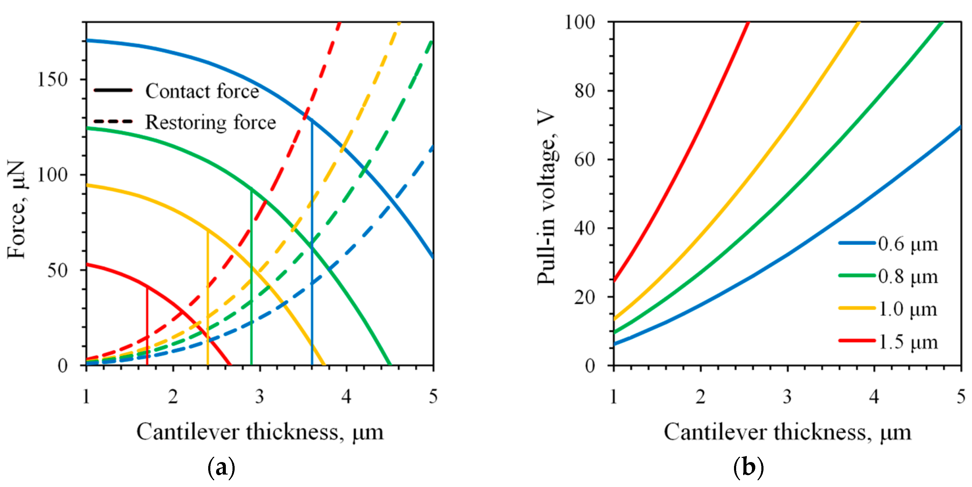
3.1. Choosing the Vertical Dimensions

The proposed strategy starts from choosing the height of the contact bump. Here and further, the calculations are performed for V = 90 V, which is a typical voltage for electrostatic switches. The dependence of Fc on h is shown in Figure 4a. Decreasing the height from 0.5 to 0.1 µm increases the contact force from 10 to 50 µN. The growth is explained by an increase in the electrostatic force due to a drop of the distance between the cantilever and the electrode in the closed state. For h from 0.2 to 0.5 µm, the analytical results agree with FEM predictions. However, for h = 0.1 µm, the simulation provides Fc = 89 µN, which is almost two times higher in comparison with analytics. This discrepancy is determined by buckling of the cantilever toward the electrode, which is not taken into account in the analytical model. Decreasing h linearly increases the restoring force from 18 to 26 µN, as shown in Figure 4a.
Lowering the bump height drops the collapse voltage from 280 to 120 V, as demonstrated in Figure 4b. The inset of this graph shows the shape of the collapsed cantilever. For h = 0.1 µm, this voltage comes close to the driving value, but h = 0.2 µm provides a significantly higher voltage Vcollapse = 220 V. Therefore, the range from 0.2 to 0.5 µm ensures safe operation of the switch. For this range, the strongest forces Fc = 32 µN and Fr = 24 µN are achieved at h = 0.2 µm, so this value is considered as an optimal height, which is used in further calculations.
The next step is the selection of the cantilever thickness and air gap. The dependence of Fc and Fr on t for various values of g0 is demonstrated in Figure 5a. For the initial thickness t = 2.0 µm, decreasing the gap from 1.5 to 0.6 µm raises the contact force from 32 to 164 µN, but the restoring force drops from 24 to 7 µN. This drop has to be compensated for stable overcoming of stiction. The compensation is easily achieved by increasing the cantilever thickness, because k~t3. But the growth of the restoring force reduces the contact force, according to Equation (11). Therefore, one has to choose the values of g0 and t, which satisfy the conditions Fc ≥ 100 µN and Fr Fc/3. The first condition is possible only for the gap of 0.6 and 0.8 µm, as shown in Figure 5a. The second relation is valid for the values of t located to the right of the vertical lines marked on this graph. For g0 = 0.8 µm, the minimal thickness is of 2.9 µm. But in this case Fc = 92 µm, so the first condition is not satisfied. For g0 = 0.6 µm, the minimal thickness is equal to 3.6 µm. The forces are Fc = 128 µN and Fr = 43 µN, so both conditions are fulfilled, and this gap is suitable. Nevertheless, the thickness can be slightly increased in order to raise the restoring force and ensure the margin of reliability. For t = 4.0 µm, the switch develops contact and restoring forces of 112 and 59 µN, respectively. FEM simulation provides Fc = 109 µN and confirms the validity of the analytical model.
The dependence of the pull-in voltage on the cantilever thickness for different gaps is shown in Figure 5b. Reducing g0 significantly lowers Vpull-in, while increasing t raises Vpull-in due to increasing k. The initial switch with g0 = 1.5 µm and t = 2.0 µm demonstrates Vpull-in = 70 V, while the optimized device with g0 = 0.6 µm and t = 4.0 µm is actuated at Vpull-in = 50 V. Thus, manipulation of the vertical dimensions enhances the forces without increasing the operating voltage. It is worth noting that decreasing g0 from 1.5 to 0.6 µm and increasing t from 2.0 to 4.0 µm slightly lowers the collapse voltage from 220 to 200 V. However, Vcollapse still significantly exceeds the driving voltage and ensures safe operation.
Choosing the vertical size increases Fc from 10 to 112 µN, i.e., by more than an order of magnitude. With such a force, an elastic deformation of the contact material takes place. According to Equations (1) and (2), the growth of Fc should reduce the contact resistance by 2.2 times. However, this assumption is valid for clean surfaces. For real contacts, exceeding the threshold of 100 µN allows one to expect a more significant decrease in Rc [29,30,31,33,38] and its stabilization due to the breaking of contaminating films. The restoring force grows from 18 to 59 µN and is approximately half of Fc, which ensures a reliable overcoming of stiction. An additional benefit is the reduction in Vpull-in from 70 to 50 V. These results are achieved by reducing the bump height from 0.5 to 0.2 µm and the gap from 1.5 to 0.6 µm as well as by increasing the cantilever thickness from 2.0 to 4.0 µm. The switch design is not modified principally, and the lateral size remains compact. The switch can be fabricated with the technical process established by authors [58]. The route does not require any changes except the time for deposition and etching of structural materials.

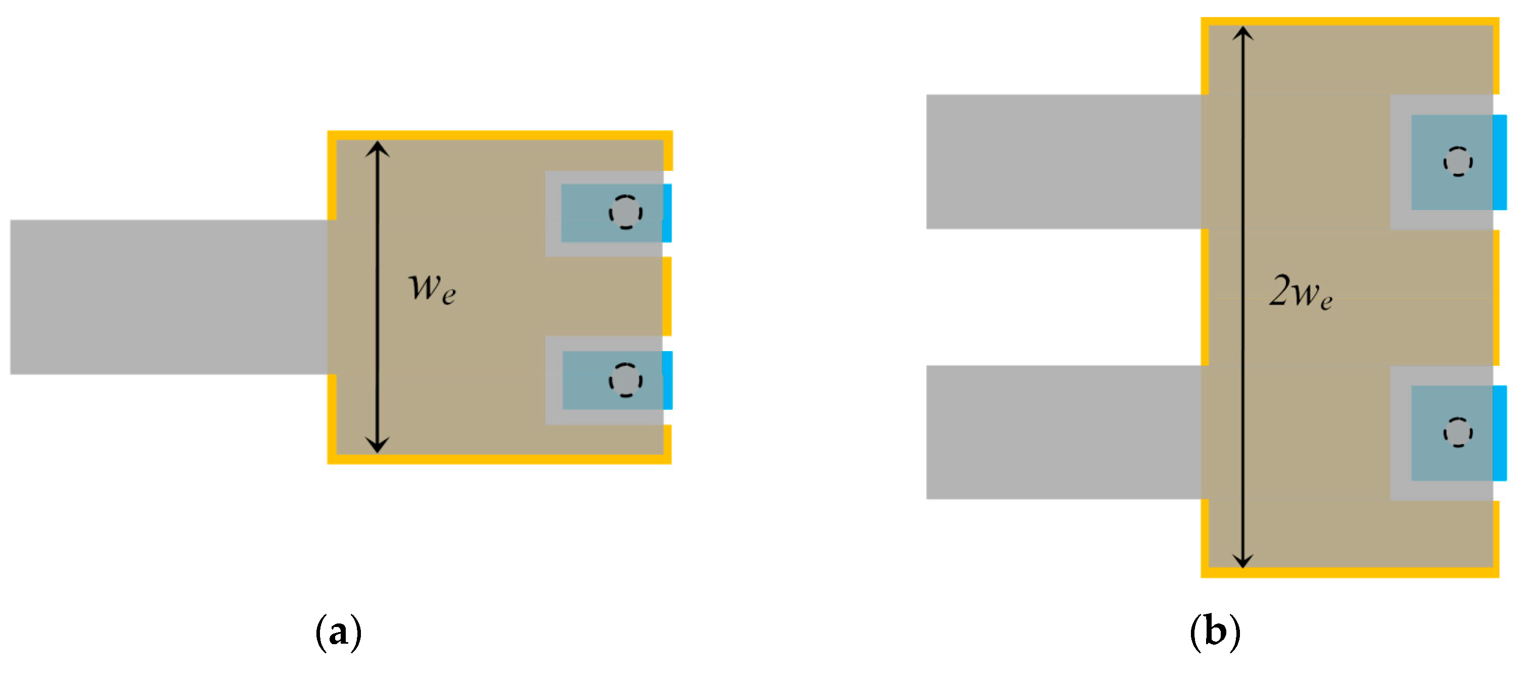
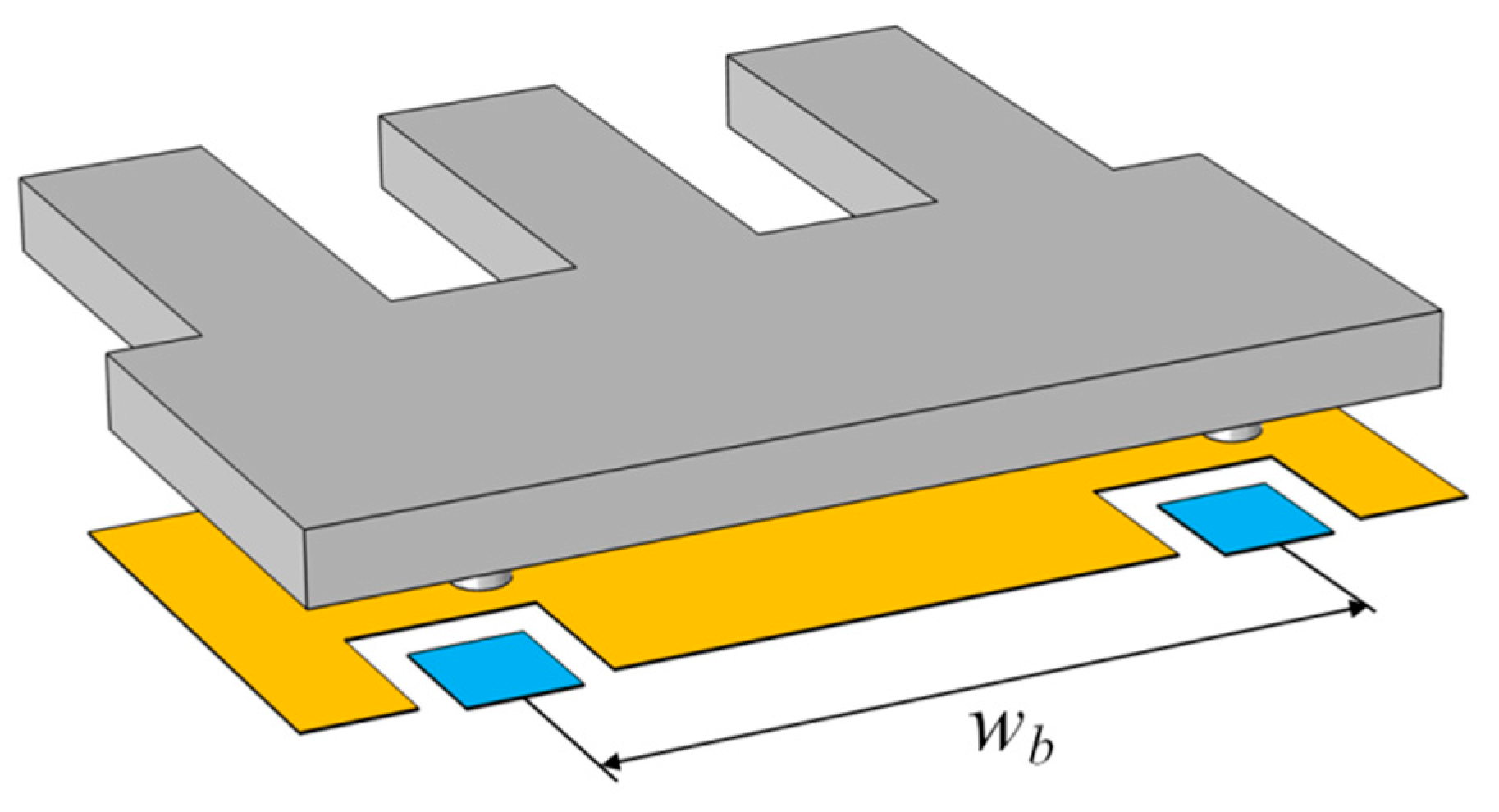
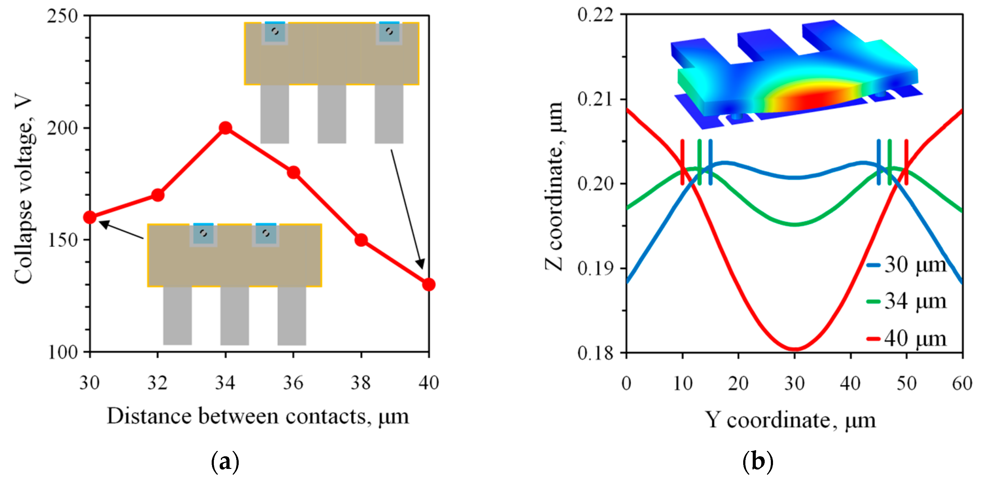
3.2. Double Cantilever Design

The cantilever with one contact bump touches the signal electrode at the point located on the longitudinal axis of symmetry. This design allows twisting of the cantilever around this axis. The twist may occur under the electrostatic torque arising when the symmetry is broken, e.g., in case of the lithographic misalignment during fabrication. As a result, the cantilever may touch the driving electrode and fail due to a short circuit. To prevent the twist, the cantilever is commonly equipped with two bumps, as shown in Figure 6a. However, this approach distributes the contact force between the bumps, so the force per contact is reduced two times and goes below 100 µN.
To keep the force per contact at the high level, it is proposed to use the switch shown in Figure 6b. It is designed by combining two basic switches in parallel. The cantilever consists of two beams connected by their widened parts and has the width of 2we. It has two fixed regions and two bumps, which increase stability in the bottom position. The force per bump remains unchanged and equal to 112 µN, while the total contact force Fc,total = 2Fc = 224 µN is doubled. The restoring force Fr,total = 2Fr = 118 µN also grows two times compared to a single structure, because combining two cantilevers doubles the stiffness. The pull-in voltage does not change, since the growth of k is compensated by the enlargement of A. It is important to note that the double switch should have two times lower contact resistance due to doubling the contact area. The dual design was first introduced by Northeastern University [59] and elaborated in several papers [47,48,49]. Thanks to high reliability, it was transformed by Radant MEMS to one of the most successful switches on the MEMS market [60]. However, the underlying reasons for choosing the cantilever shape and size were not explained.

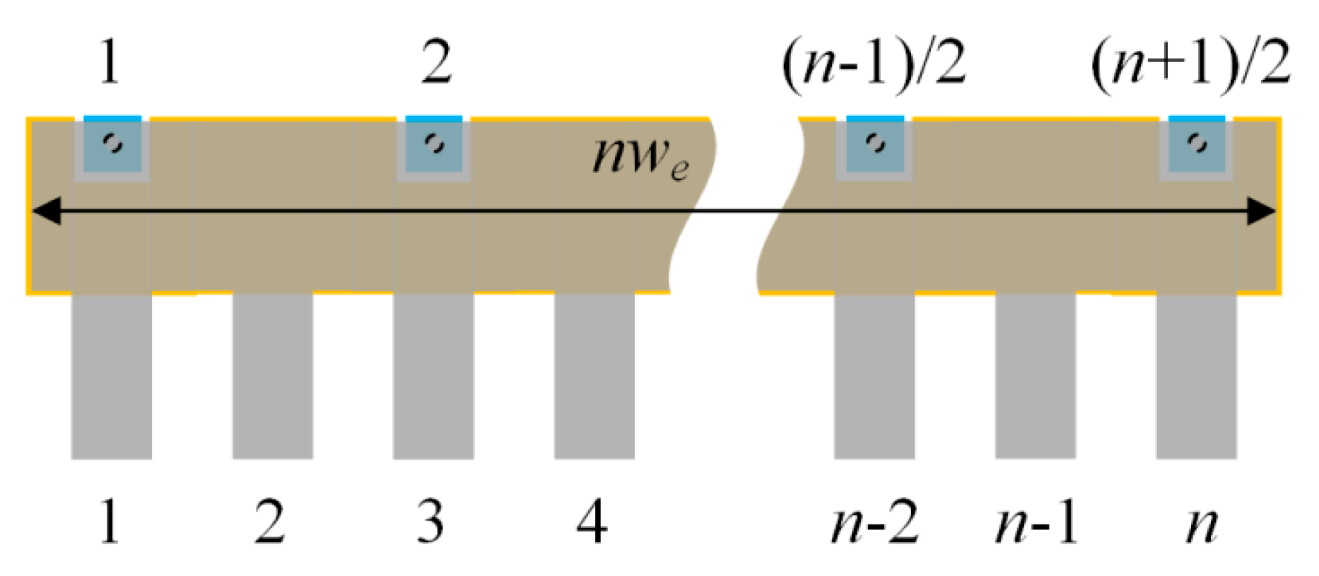
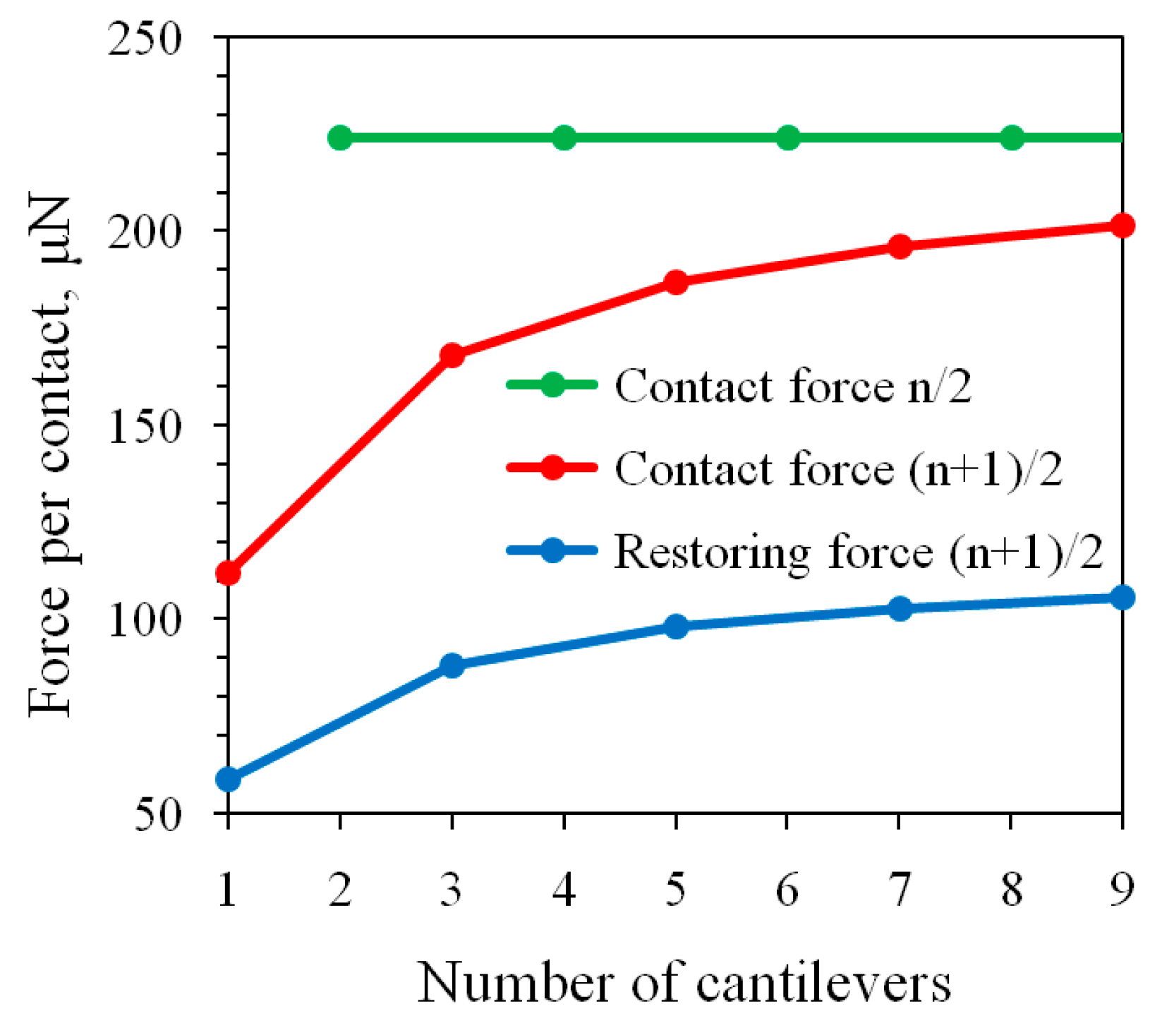
3.3. Multiple Cantilever Design

The properties of the dual switch can be extrapolated to the device consisting of n basic structures. The total contact force increases n times:
F c , t o t a l = n F c .
The advantage of this approach is a significant increase in the contact area due to the use of n bumps, but the specific force remains the same as for the single switch. To increase the force per contact, one has to distribute the total force to a smaller number of contacts, i.e., to remove some bumps. Figure 7 shows the switch containing n united cantilevers and (n +1)/2 contacts. In such a configuration, every second beam has a bump. The outside cantilevers are necessarily equipped with contacts to avoid touching the driving electrode, so n takes odd values.
The force per bump is determined as follows:
F c , b u m p = F c , t o t a l ( n + 1 ) / 2 = 2 n n + 1 F c .
For a large number of cantilevers, the specific force tends to double in comparison with the basic switch. The dependence of Fc,bump on n is shown in Figure 8. The number of beams varies from 1 to 9, while the number of contacts takes the value from 1 to 5, according to the rule (n +1)/2. The switch with n = 3 develops Fc,bump = 168 µN, which is 1.5 times higher compared to the basic design with n = 1. Increasing the number of cantilevers to n = 9 raises the specific force to 202 µN. But it should be noted that the growth of Fc,bump slows down with increasing n. The cantilever with the large number of bumps may provide unequal force distribution among contacts due to the technological variation in the bump height. In addition, using multiple cantilevers increases the lateral size of the switch. An optimal case is the triple cantilever with two bumps, as schematically illustrated in Figure 9. It provides a uniform distribution of forces and has the reasonable width of 60 µm.
Similar considerations are valid for the restoring force. Combining n switches proportionally increases the total force:
F r , t o t a l = n F r .
If every second bump is removed, the restoring force per contact is written as follows:
F r , b u m p = F r , t o t a l ( n + 1 ) / 2 = 2 n n + 1 F r
The specific force approaches 2Fr with increasing n. The dependence of Fr,bump on n is depicted in Figure 8. As for the contact force, the growth of the restoring force slows down with increasing the number of beams. The largest increment takes place for the transition from n = 1 to n = 3. The optimal switch with the triple cantilever provides Fr,bump = 88 µN.
Removing the bumps reduces the number of supporting points for the cantilever in the bottom position and increases its deformation between the bumps. As a result, the collapse voltage drops from 200 to 130 V and approaches the driving value. However, for the three-beam two-bump switch, one can restore Vcollapse by varying the distance between the bumps wb indicated in Figure 9. The dependence of Vcollapse on wb is shown in Figure 10a. Initially, the distance is equal to 40 µm, and the collapse takes place at V = 130 V. The deformation of the cantilever is concentrated between the contacts, as demonstrated in Figure 10b. Reducing wb to 34 µm lowers the deformation of the central part and raises Vcollapse to 200 V. Further reducing the distance drops the collapse voltage again due to the excessive bending of the cantilever edges. Thus, wb = 34 µm is an optimal value, which provides the same collapse voltage as for the basic single-beam design.
Another option is to connect the number of cantilevers and contacts by a rule n/2, where n ≥ 2 and takes even values. In this case, the contact force per bump is two times higher compared to the basic design and is equal to 224 μN. The dependence of Fc,bump on n is a horizontal line shown in Figure 8 by green color. The switch with four cantilevers and two contacts develops a 30% higher specific force than the triple cantilever with two bumps. However, it has the collapse voltage of 90 V or lower, depending on the position of bumps. This value is close to the pull-in voltage, and safe operation of the switch is not ensured. This situation takes place for all the switches designed according to the rule n/2. Therefore, the rule (n +1)/2 is optimal.
Thus, the triple cantilever with two bumps is considered as an optimal design. It provides a specific contact and restoring force of 168 and 88 µN, respectively, which is 50% higher in comparison with the single-beam device. The first and second pull-in voltages are of 50 and 200 V, and they are the same as for the singe switch. Two bumps prevent twisting of the cantilever and uniformly distribute the forces between contacts. The switch keeps the optimized vertical dimensions and has a miniature footprint of 50 × 60 µm. To the authors’ knowledge, this is the most compact switch that provides such a high contact force. Furthermore, it is planned to fabricate this device using the established technology [58] and to verify its operation.
Multi-cantilever switches are poorly discussed in the literature. An array of 10 and 20 independent cantilevers was proposed in the work [46]. The switching module with several individual beams is demonstrated in [29]. These structures reduce the overall switch resistance and keep the merits of a tiny device, including stress robustness and low switching time. However, united cantilevers with a reduced number of bumps were not considered. The present work clearly explains the advantages of such structures.
A lot of works are devoted to designing MEMS switches. However, most of them do not consider the contact force as an important characteristic of the actuator. The importance of Fc is highlighted in the papers [39,40,41,42,43,44,45,50,56,57]. However, in these works, the force is increased by enlarging lateral dimensions of the electrodes. In particular, the movable plate of the switch from [39] has a size of about 500 µm. The innovation of the present work is that it describes the way to increase Fc of a compact switch. A device with a 50 µm long cantilever and a specific contact force of more than 150 µN has not been described previously. The parallel connection of several cantilevers and choosing the number and position of contact bumps is also proposed for the first time.

4. Conclusions

The paper presents a comprehensive approach for increasing the contact and restoring force of an electrostatically actuated cantilever-type MEMS switch. It is based on analytical calculations, which are verified and supported by FEM simulation. The strategy is applied to a compact device equipped by an aluminum cantilever with a length of 50 µm and a width of 20 µm. Manipulating its vertical dimensions increases the contact force from 10 to 112 µN, making the actuator strong enough to provide low and stable contact resistance. The restoring force is increased from 18 to 59 µN. It is more than half of the contact force and ensures reliable de-actuation. The growth of forces is accompanied by a reduction in the pull-in voltage from 70 to 50 V. The collapse voltage is equal to 200 V and significantly exceeds the operating value. The principle design of the switch is not changed during optimization, so the fabrication route requires minor corrections. Further modification includes connecting several switches in parallel and reducing the number of bumps. This technique additionally increases the contact and restoring forces and improves the mechanical stability of the cantilever. An optimal device contains the triple cantilever and two bumps. It develops 50% higher forces per contact in comparison with the single structure and the same pull-in voltage. Adjusting the distance between contacts restores the collapse voltage to 200 V. The triple cantilever has the length of 50 µm, while the width is increased to 60 µm. Nevertheless, the switch still keeps the advantages of a miniature device. The proposed strategy contains design rules for building reliable MEMS switches. It can be applied to devices of various sizes and the ratio of the contact and restoring forces.

Author Contributions

Conceptualization, I.V.U.; methodology, I.A.B.; validation, I.V.U. and I.A.B.; investigation, I.A.B.; writing—original draft preparation, I.A.B.; writing—review and editing, I.V.U.; visualization, I.A.B.; supervision, I.V.U. All authors have read and agreed to the published version of the manuscript.

Funding

This research was funded by Program No. FFNN-2022-0017 of the Ministry of Science and Higher Education of Russia for Valiev Institute of Physics and Technology of RAS.

Institutional Review Board Statement

Not applicable.

Informed Consent Statement

Not applicable.

Data Availability Statement

Data are contained within the article.

Conflicts of Interest

The authors declare no conflicts of interest. The funders had no role in the design of the study; in the collection, analyses, or interpretation of data; in the writing of the manuscript; or in the decision to publish the results.

References

  1. Rebeiz, G.M.; Patel, C.D.; Han, S.K.; Ko, C.-H.; Ho, K.M.J. The search for a reliable MEMS switch. IEEE Microw. Mag. 2013, 14, 57–67. [Google Scholar] [CrossRef]
  2. Iannacci, J. RF-MEMS for high-performance and widely reconfigurable passive components—A review with focus on future telecommunications, Internet of Things (IoT) and 5G applications. J. King Saud Univ. 2017, 29, 436–443. [Google Scholar] [CrossRef]
  3. Shekhar, S.; Vinoy, K.J.; Ananthasuresh, G.K. Low-voltage high-reliability MEMS switch for millimeter wave 5G applications. J. Micromech. Microeng. 2018, 28, 075012. [Google Scholar] [CrossRef]
  4. Ma, L.-Y.; Soin, N.; Daut, M.H.M.; Hatta, S.F.W.M. Comprehensive study on RF-MEMS switches used for 5G scenario. IEEE Access 2019, 7, 107506. [Google Scholar] [CrossRef]
  5. Rao, K.R.; Kumar, P.A.; Guha, K.; Sailaja, B.V.S.; Vineetha, K.V.; Baishnab, K.L.; Sravani, K.G. Design and simulation of fixed-fixed flexure type RF MEMS switch for reconfigurable antenna. Microsyst. Technol. 2021, 27, 455–462. [Google Scholar] [CrossRef]
  6. Xu, Y.; Tian, Y.; Zhang, B.; Duan, J.; Yan, L. A novel RF MEMS switch on frequency reconfigurable antenna application. Microsyst. Technol. 2018, 24, 3833–3841. [Google Scholar] [CrossRef]
  7. Haupt, R.L.; Lanagan, M. Reconfigurable antennas. IEEE Antennas Propag. Mag. 2013, 55, 49–61. [Google Scholar] [CrossRef]
  8. Haider, N.; Caratelli, D.; Yarovoy, A.G. Recent developments in reconfigurable and multiband antenna technology. Int. J. Antennas Propag. 2013, 2013, 869170. [Google Scholar] [CrossRef]
  9. Zhou, W.; Sheng, W.; Cui, J.; Han, Y.; Ma, X.; Zhang, R. SR-Crossbar topology for large-scale RF MEMS switch matrices. IET Microw. Antennas Propag. 2019, 13, 231–238. [Google Scholar] [CrossRef]
  10. Daneshmand, M.; Mansour, R.R. RF MEMS satellite switch matrices. IEEE Microw. Mag. 2011, 12, 92–109. [Google Scholar] [CrossRef]
  11. Cao, T.; Hu, T.; Zhao, Y. Research status and development trend of MEMS switches: A review. Micromachines 2020, 11, 694. [Google Scholar] [CrossRef] [PubMed]
  12. Kurmendra; Kumar, R. A review on RF micro-electro-mechanical-systems (MEMS) switch for radio frequency applications. Microsyst. Technol. 2021, 27, 2525–2542. [Google Scholar] [CrossRef]
  13. Gaddi, R.; Van Kampen, R.; Unamuno, A.; Joshi, V.; Lacey, D.; Renault, M.; Smith, C.; Knipe, R.; Yost, D. MEMS technology integrated in the CMOS back end. Microelectron. Reliab. 2010, 50, 1593–1598. [Google Scholar] [CrossRef]
  14. Dai, C.-L.; Chen, J.-H. Low voltage actuated RF micromechanical switches fabricated using CMOS-MEMS technique. Microsyst. Technol. 2006, 12, 1143–1151. [Google Scholar] [CrossRef]
  15. Dey, S.; Koul, S.K. Design and development of a CPW-based 5-bit switched-line phase shifter using inline metal contact MEMS series switches for 17.25 GHz transmit/receive module application. J. Micromech. Microeng. 2014, 24, 015005. [Google Scholar] [CrossRef]
  16. Sharma, A.K.; Gautam, A.K.; Farinelli, P.; Dutta, A.; Singh, S.G. A Ku band 5 bit MEMS phase shifter for active electronically steerable phased array applications. J. Micromech. Microeng. 2015, 25, 035014. [Google Scholar] [CrossRef]
  17. Gong, S.; Shen, H.; Barker, N.S. A 60-GHz 2-bit switched-line phase shifter using SP4T RF-MEMS switches. IEEE Trans. Microw. Theory Tech. 2011, 59, 894–900. [Google Scholar] [CrossRef]
  18. Park, J.-H.; Lee, S.; Kim, J.-M.; Kim, H.-T.; Kwon, Y.; Kim, Y.-K. Reconfigurable millimeter-wave filters using CPW-based periodic structures with novel multiple-contact MEMS switches. J. Microelectromech. Syst. 2005, 14, 456–463. [Google Scholar] [CrossRef]
  19. Peroulis, D.; Pacheco, S.; Sarabandi, K.; Katehi, L.P.B. Tunable lumped components with applications to reconfigurable MEMS filters. In Proceedings of the 2001 IEEE MTT-S International Microwave Sympsoium, Phoenix, AZ, USA, 20–24 May 2001. [Google Scholar] [CrossRef]
  20. Li, M.; Zhang, Y.; Zhao, Y.; Xue, P.; Wu, Q. Design and fabrication of a 4-bit RF MEMS attenuator with a high attenuation accuracy. Analog Integr. Circ. Sig. Process. 2020, 102, 617–624. [Google Scholar] [CrossRef]
  21. Iannacci, J.; Tschoban, C. RF-MEMS for future mobile applications: Experimental verification of a reconfigurable 8-bit power attenuator up to 110 GHz. J. Micromech. Microeng. 2017, 27, 044003. [Google Scholar] [CrossRef]
  22. Guo, X.; Gong, Z.; Zhong, Q.; Liang, X.; Liu, Z. A miniaturized reconfigurable broadband attenuator based on RF MEMS switches. J. Micromech. Microeng. 2016, 26, 074002. [Google Scholar] [CrossRef]
  23. Heredia, J.; Ribó, M.; Pradell, L.; Wipf, S.T.; Göritz, A.; Wietstruck, M.; Wipf, C.; Kaynak, M. A 125–143-GHz frequency-reconfigurable BiCMOS compact LNA using a single RF-MEMS switch. IEEE Microw. Compon. Lett. 2019, 29, 339–341. [Google Scholar] [CrossRef]
  24. van Spengen, W.M.; Roobol, S.B.; Klaassen, W.P.; Oosterkamp, T.H. The MEMSamp: Using (RF-)MEMS switches for the micromechanical amplification of electronic signals. J. Micromech. Microeng. 2010, 20, 125011. [Google Scholar] [CrossRef]
  25. Saleem, M.M.; Nawaz, H. A systematic review of reliability issues in RF-MEMS switches. Micro Nanosyst. 2019, 11, 11–33. [Google Scholar] [CrossRef]
  26. Huang, Y.; Vasan, A.S.S.; Doraiswami, R.; Osterman, M.; Pecht, M. MEMS reliability review. IEEE Trans. Device Mater. Reliab. 2012, 12, 482–493. [Google Scholar] [CrossRef]
  27. Toler, B.F.; Coutu, R.A.; McBride, J.W. A review of micro-contact physics for microelectromechanical systems (MEMS) metal contact switches. J. Micromech. Microeng. 2013, 23, 103001. [Google Scholar] [CrossRef]
  28. Basu, A.; Adams, G.G.; McGruer, N.E. A review of micro-contact physics, materials, and failure mechanisms in direct-contact RF MEMS switches. J. Micromech. Microeng. 2016, 26, 104004. [Google Scholar] [CrossRef]
  29. Ma, Q.; Tran, Q.; Chou, T.-K.A.; Heck, J.; Bar, H.; Kant, R.; Rao, V. RF Metal contact reliability of RF MEMS switches. Proc. SPIE 2007, 6463, 646305. [Google Scholar] [CrossRef]
  30. Broue, A.; Fourcade, T.; Dhennin, J.; Courtade, F.; Charvet, P.-L.; Pons, P.; Lafontan, X.; Plana, R. Validation of bending tests by nanoindentation for micro-contact analysis of MEMS switches. J. Micromech. Microeng. 2010, 20, 085025. [Google Scholar] [CrossRef]
  31. Broue, A.; Dhennin, J.; Charvet, P.-L.; Pons, P.; Ben Jemaa, N.; Heeb, P.; Coccetti, F.; Plana, R. Comparative study of RF MEMS micro-contact materials. Int. J. Microw. Wirel. Technol. 2012, 4, 413–420. [Google Scholar] [CrossRef]
  32. Yamashita, T.; Itoh, T.; Suga, T. Investigation of anti-stiction coating for ohmic contact MEMS switches with thiophenol and 2-naphthalenethiol self-assembled monolayer. Sens. Actuators A 2011, 172, 455–461. [Google Scholar] [CrossRef]
  33. Chen, L.; Guo, Z.J.; Joshi, N.; Eid, H.; Adams, G.G.; McGruer, N.E. An improved SPM-based contact tester for the study of microcontacts. J. Micromech. Microeng. 2012, 22, 045017. [Google Scholar] [CrossRef]
  34. Schimkat, J. Contact measurements providing basic design data for microrelay actuators. Sens. Actuators A 1999, 73, 138–143. [Google Scholar] [CrossRef]
  35. Kwon, H.; Park, J.-H.; Lee, H.-C.; Choi, D.-J.; Park, Y.-H.; Nam, H.-J.; Joo, Y.-C. Investigation of similar and dissimilar metal contacts for reliable radio frequency micorelectromechanical switches. Jpn. J. Appl. Phys. 2008, 47, 6558–6562. [Google Scholar] [CrossRef]
  36. Coutu, R.A.; Tomer, D. Micro-contacts testing using a micro-force sensor compatible with biological systems. Int. J. Biosens. Bioelectron. 2017, 3, 00052. [Google Scholar] [CrossRef]
  37. Bull, T.G.; McBride, J.W. In-situ contact surface characterization in a MEMS ohmic switch under low current switching. Technologies 2018, 6, 47. [Google Scholar] [CrossRef]
  38. Mahanta, P.; Anwar, F.; Coutu, R.A. Novel test fixture for characterizing MEMS switch microcontact reliability and performance. Sensors 2019, 19, 579. [Google Scholar] [CrossRef]
  39. Kim, S.-B.; Yoon, Y.-H.; Lee, Y.-B.; Choi, K.-W.; Jo, M.-S.; Min, H.-W.; Yoon, J.-B. 4 W power MEMS relay with extremely low contact resistance: Theoretical analysis, design and demonstration. J. Microelectromech. Syst. 2020, 29, 1304–1313. [Google Scholar] [CrossRef]
  40. Kim, S.-B.; Min, H.-W.; Lee, Y.-B.; Kim, S.-H.; Choi, P.-K.; Yoon, J.-B. Utilizing mechanical adhesion force as a high contact force in a MEMS relay. Sens. Actuators A 2021, 331, 112894. [Google Scholar] [CrossRef]
  41. Blondy, P.; Pothier, A.; Stefanini, R.; Gauvin, J.; Passerieux, D.; Vendier, O.; Courtade, F. Development of an all-metal large contact force reliable RF-MEMS relay for space applications. In Proceedings of the 42nd European Microwave Conference, Amsterdam, The Netherlands, 29 October–1 November 2012. [Google Scholar] [CrossRef]
  42. Patel, C.D.; Rebeiz, G.M. A high-reliability high-linearity high-power RF MEMS metal-contact switch for DC-40-GHz applications. IEEE Trans. Microw. Theory Tech. 2012, 60, 3096–3112. [Google Scholar] [CrossRef]
  43. Patel, C.D.; Rebeiz, G.M. RF MEMS metal-contact switches with mN-contact and restoring forces and low process sensitivity. IEEE Trans. Microw. Theory Tech. 2011, 59, 1230–1237. [Google Scholar] [CrossRef]
  44. Seki, T.; Uno, Y.; Narise, K.; Masuda, T.; Inoue, K.; Sato, S.; Sato, F.; Imanaka, K.; Sugiyama, S. Development of a large-force low-loss metal-contact RF MEMS switch. Sens. Actuators A 2006, 132, 683–688. [Google Scholar] [CrossRef]
  45. Sedaghat-Pisheh, H.; Rebeiz, G.M. Variable spring constant, high contact force RF MEMS switch. In Proceedings of the 2010 IEEE MTT-S International Microwave Symposium, Anaheim, CA, USA, 23–28 May 2010. [Google Scholar] [CrossRef]
  46. Stefanini, R.; Chatras, M.; Blondy, P.; Rebeiz, G.M. Miniature MEMS switches for RF applications. J. Microelectromech. Syst. 2011, 20, 1324–1335. [Google Scholar] [CrossRef]
  47. Spasos, M.; Nilavalan, R. Resistive damping implementation as a method to improve controllability in stiff ohmic RF-MEMS switches. Microsyst. Technol. 2013, 19, 1935–1943. [Google Scholar] [CrossRef]
  48. Liu, B.; Lv, Z.; He, X.; Liu, M.; Hao, Y.; Li, Z. Improving performance of the metal-to-metal contact RF MEMS switch with a Pt-Au microspring contact design. J. Micromech. Microeng. 2011, 21, 065038. [Google Scholar] [CrossRef]
  49. Nishijima, N.; Hung, J.-J.; Rebeiz, G.M. Parallel-contact metal-contact RF-MEMS switches for high power applications. In Proceedings of the 17th IEEE International Conference on Micro Electro Mechanical Systems, Maastricht, The Netherlands, 25–29 January 2004. [Google Scholar] [CrossRef]
  50. Song, Y.-H.; Kim, M.-W.; Seo, M.-H.; Yoon, J.-B. A complementary dual-contact MEMS switch using a “zipping” technique. J. Microelectromech. Syst. 2014, 23, 710–718. [Google Scholar] [CrossRef]
  51. Belozerov, I.A.; Uvarov, I.V. Performance optimization of the cantilever-based MEMS switch. St. Petersburg Polytechn. Univ. J. Phys. Math. 2022, 15, 140–144. [Google Scholar]
  52. Rebeiz, G.M. RF MEMS: Theory, Design, and Technology; John Wiley & Sons, Inc.: Hoboken, NJ, USA, 2003; 512p. [Google Scholar]
  53. Kimiaeifar, A.; Tolou, N.; Barari, C.; Herder, J.L. Large deflection analysis of cantilever beam under end point and distributed loads. J. Chin. Inst. Eng. 2014, 37, 438–445. [Google Scholar] [CrossRef]
  54. Uvarov, I.V.; Kupriyanov, A.N. Stiction-protected MEMS switch with low actuation voltage. Microsyst. Technol. 2019, 25, 3243–3251. [Google Scholar] [CrossRef]
  55. Uvarov, I.V.; Kupriyanov, A.N. Investigation of characteristics of electrostatically actuated MEMS switch with an active contact breaking mechanism. Russ. Microelectron. 2018, 47, 307–316. [Google Scholar] [CrossRef]
  56. Song, Y.-H.; Kim, M.-W.; Lee, J.O.; Ko, S.-D.; Yoon, J.-B. Complementary dual-contact switch using soft and hard contact materials for achieving low contact resistance and high reliability simultaneously. J. Microelectromech. Syst. 2013, 22, 846–854. [Google Scholar] [CrossRef]
  57. Deng, P.; Wang, N.; Cai, F.; Chen, L. A high-force and high isolation metal-contact RF MEMS switch. Microsyst. Technol. 2017, 23, 4699–4708. [Google Scholar] [CrossRef]
  58. Uvarov, I.V.; Marukhin, N.V.; Naumov, V.V. Contact resistance and lifecycle of a single- and multiple-contact MEMS switch. Microsyst. Technol. 2019, 25, 4135–4141. [Google Scholar] [CrossRef]
  59. Majumder, S.; McGruer, N.E.; Adams, G.G.; Zavracky, P.M.; Morrison, R.H.; Krim, J. Study of contacts in an electrostatically actuated microswitch. Sens. Actuators A 2001, 93, 19–26. [Google Scholar] [CrossRef]
  60. Majumder, S.; Lampen, J.; Morrison, R.; Maciel, J. MEMS switches. IEEE Instrum. Meas. Mag. 2003, 6, 12–15. [Google Scholar] [CrossRef]
Figure 1. A model of contact at surface asperities.
Micro 04 00001 g001
Figure 2. The cantilever-type switch: (a) three-dimensional view; (b) top view and cross-section.
Micro 04 00001 g002
Figure 3. Schematic illustration of the cantilever cross-section in the actuated state.
Micro 04 00001 g003
Figure 4. The dependence of the contact and restoring force (a) and collapse voltage (b) on the bump height. Solid and dashed lines at the image (a) correspond to contact and restoring force, while red and blue colors indicate analytical and FEM calculations. The inset at the image (b) illustrates the deformation of the collapsed cantilever.
Micro 04 00001 g004
Figure 5. The dependence of the contact and restoring forces (a) and pull-in voltage (b) on the cantilever thickness for various values of the gap indicated by colors. Vertical lines at the image (a) mark the thickness, for which Fr is equal to Fc/3. Solid and dashed lines correspond to contact and restoring force, while different colors correspond to various values of the gap, as shown at the image (b).
Micro 04 00001 g005
Figure 6. The switch with two contact bumps located on a single cantilever (a) and on a double cantilever (b), top view.
Micro 04 00001 g006
Figure 7. The switch with n connected cantilevers and (n + 1)/2 bumps, top view.
Micro 04 00001 g007
Figure 8. The dependence of the contact and restoring force per bump on the number of cantilevers and bumps.
Micro 04 00001 g008
Figure 9. The optimal design with the triple cantilever and two bumps.
Micro 04 00001 g009
Figure 10. (a) The dependence of the collapse voltage on the distance between contacts shown by red line. The upper inset shows the switch with wb = 40 µm, while the bottom one corresponds to wb = 30 µm, as indicated by arrows. (b) Profiles of the free end of the cantilever for the different values of wb. The driving voltage is equal to 90 V. Vertical marks indicate the position of the bumps. The inset illustrates deformation of the cantilever with wb = 40 µm.
Micro 04 00001 g010
Disclaimer/Publisher’s Note: The statements, opinions and data contained in all publications are solely those of the individual author(s) and contributor(s) and not of MDPI and/or the editor(s). MDPI and/or the editor(s) disclaim responsibility for any injury to people or property resulting from any ideas, methods, instructions or products referred to in the content.

