
Structural Inhomogeneities and Nonlinear Phenomena in Charge Transfer under Cold Field Emission in Individual Closed Carbon Nanotubes

 , , ,
, , ,  and
and 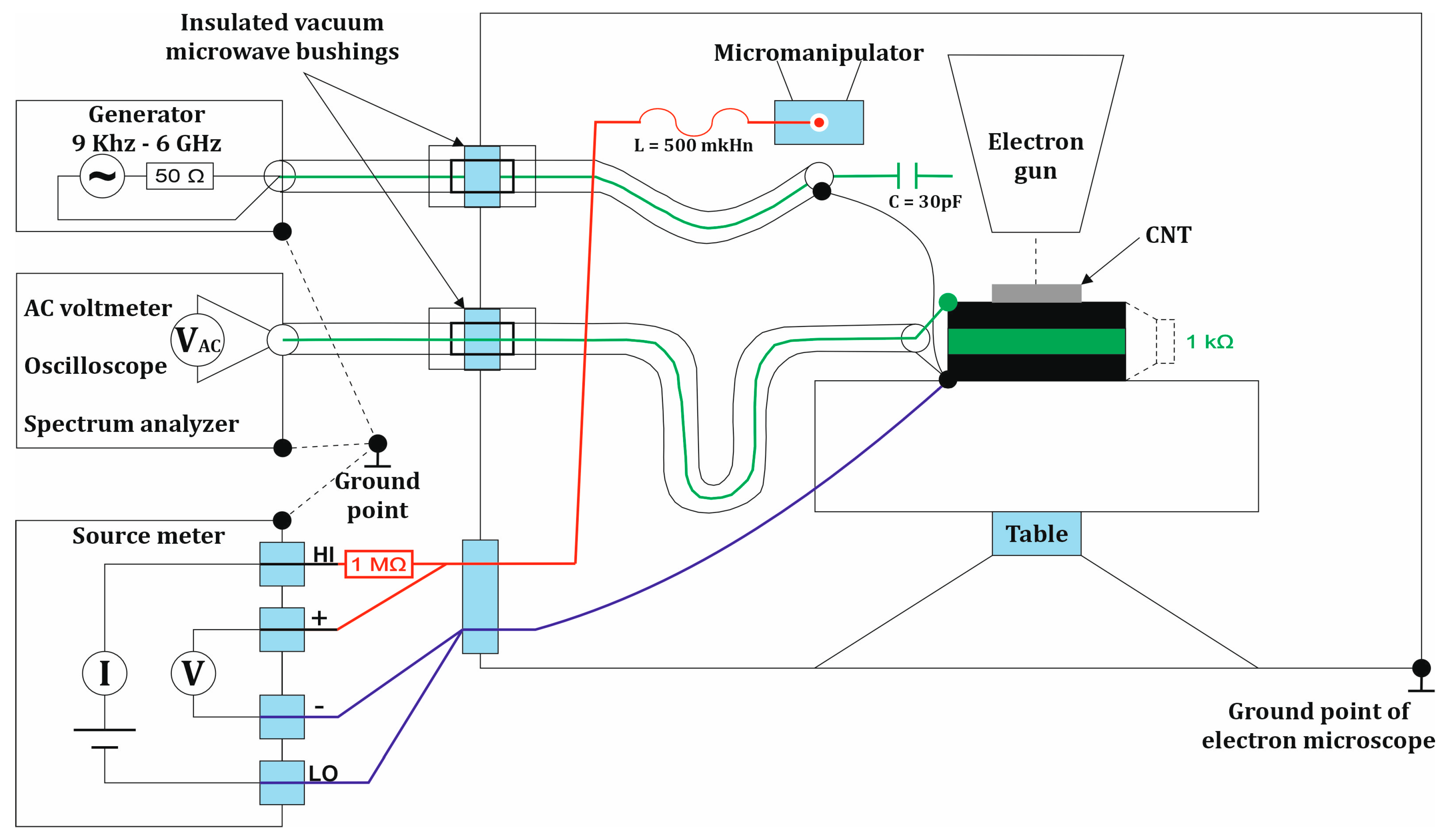
Abstract
:1. Introduction
2. Materials and Methods
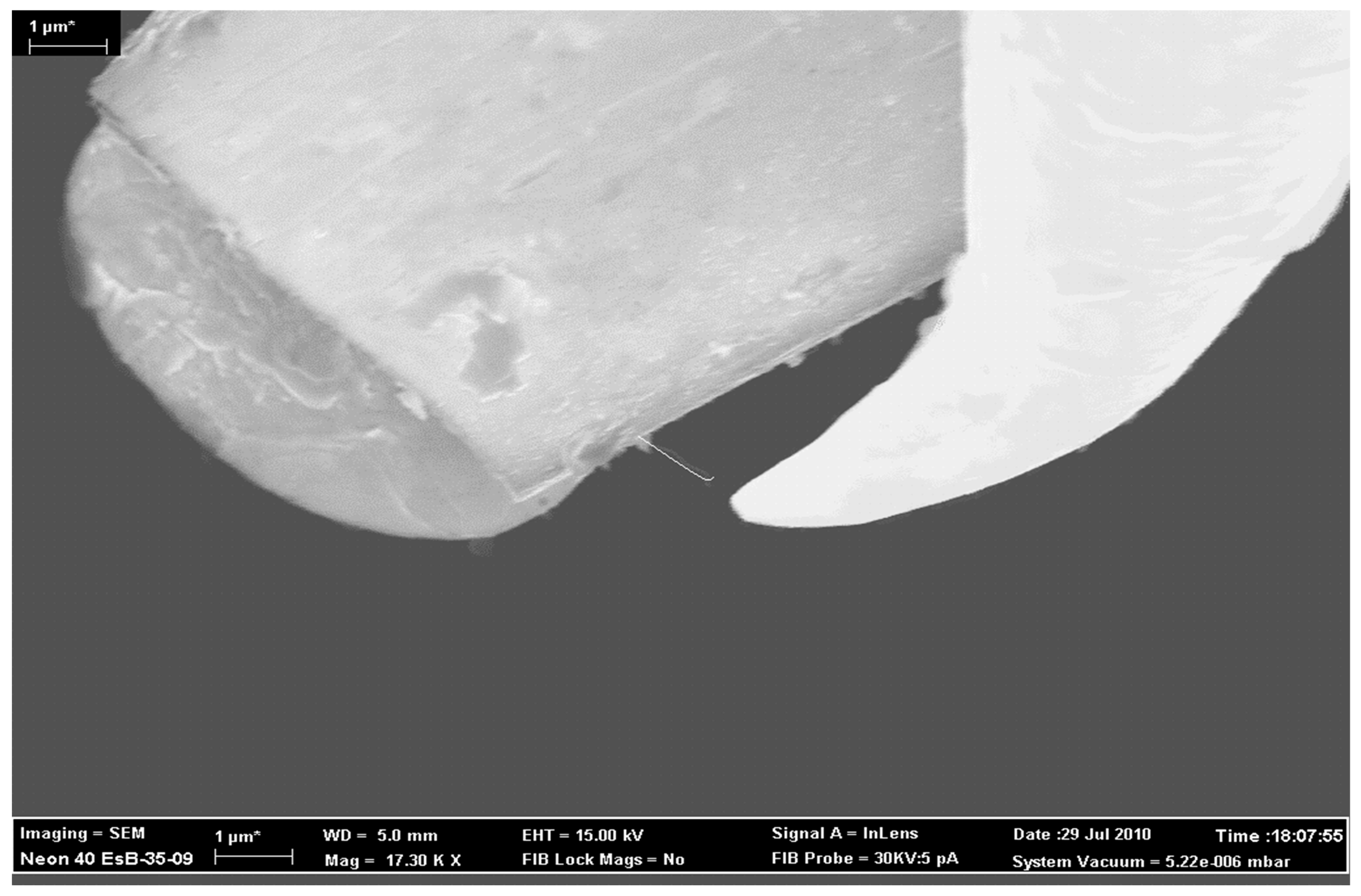
Microscopy Measurements Methods
3. Experimental Results
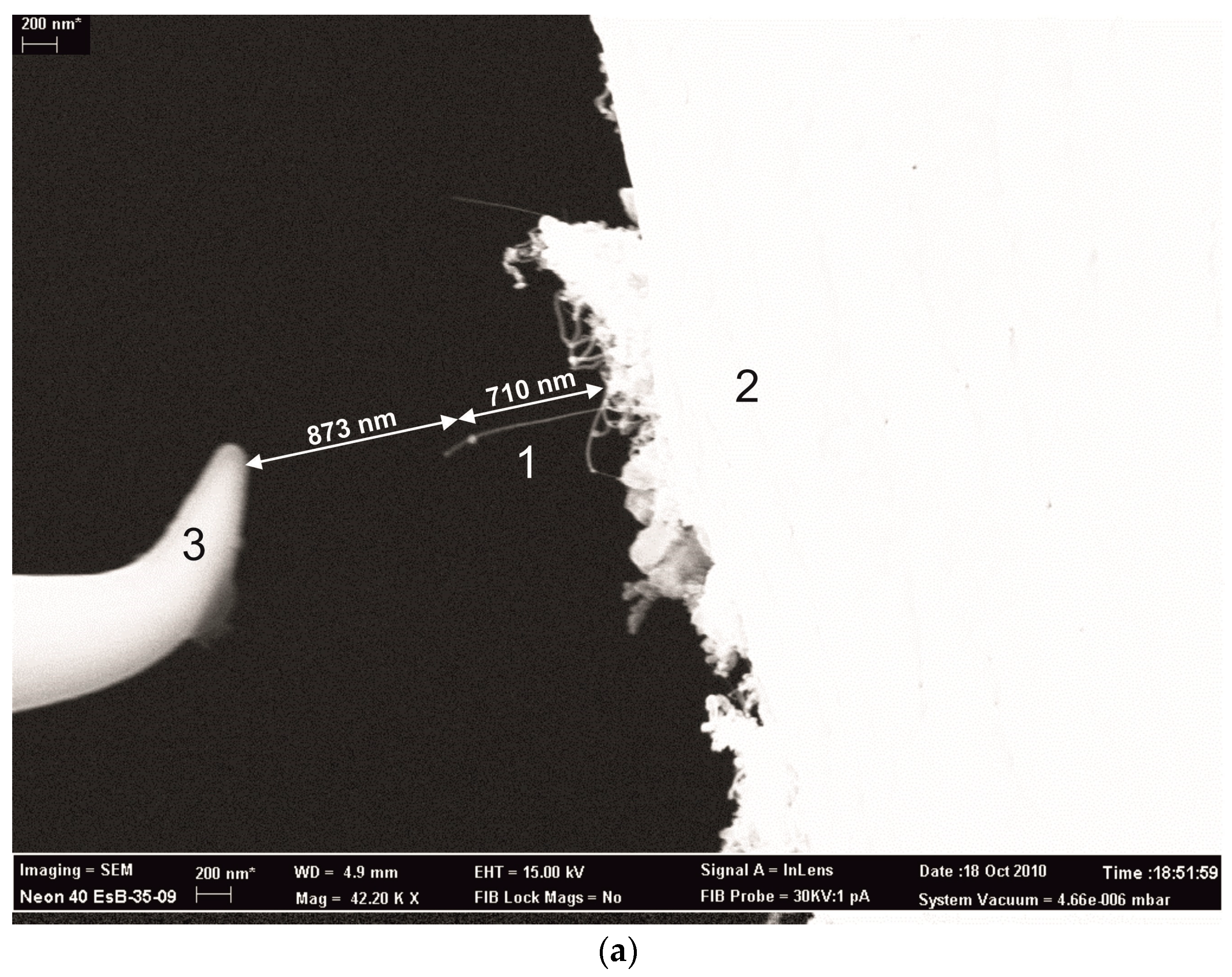
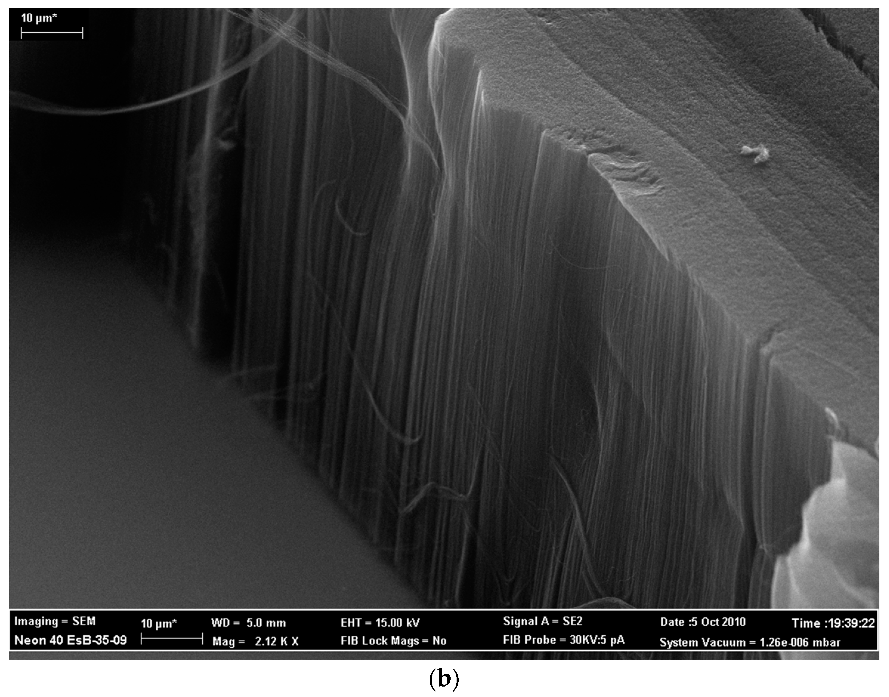
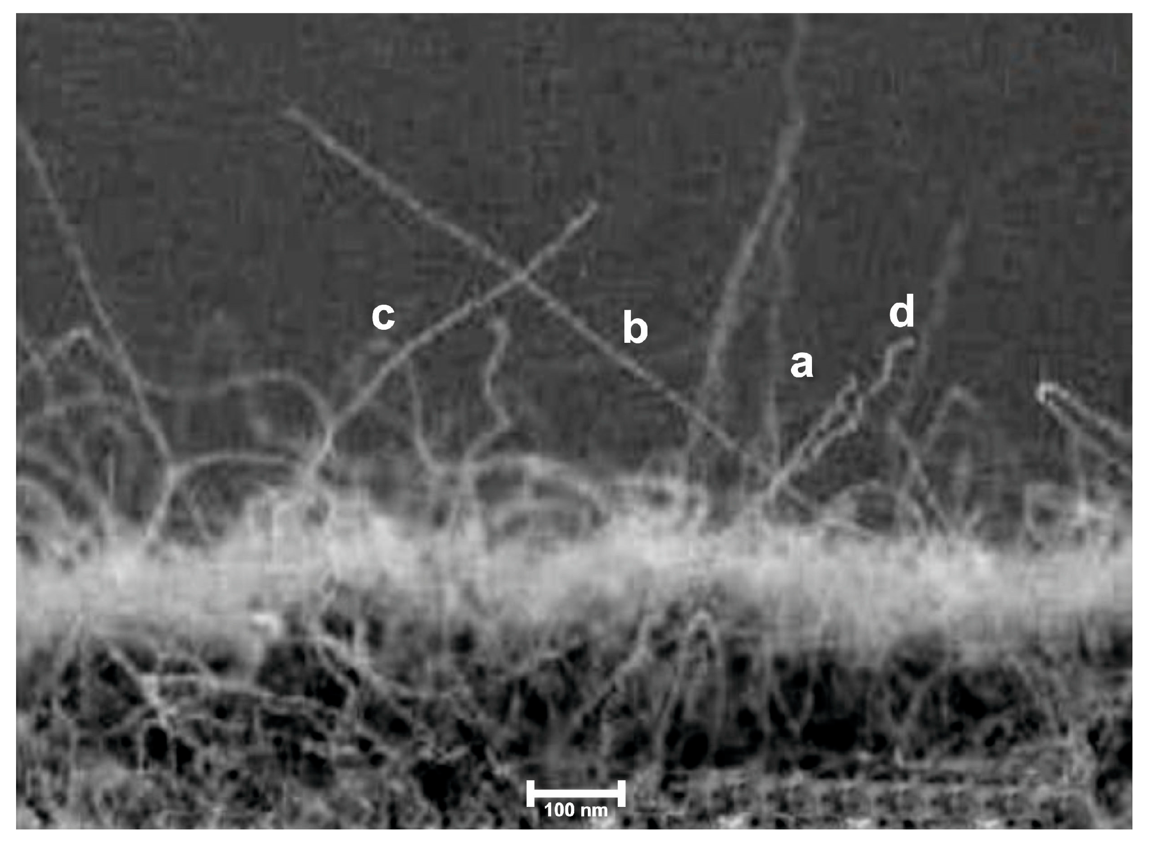
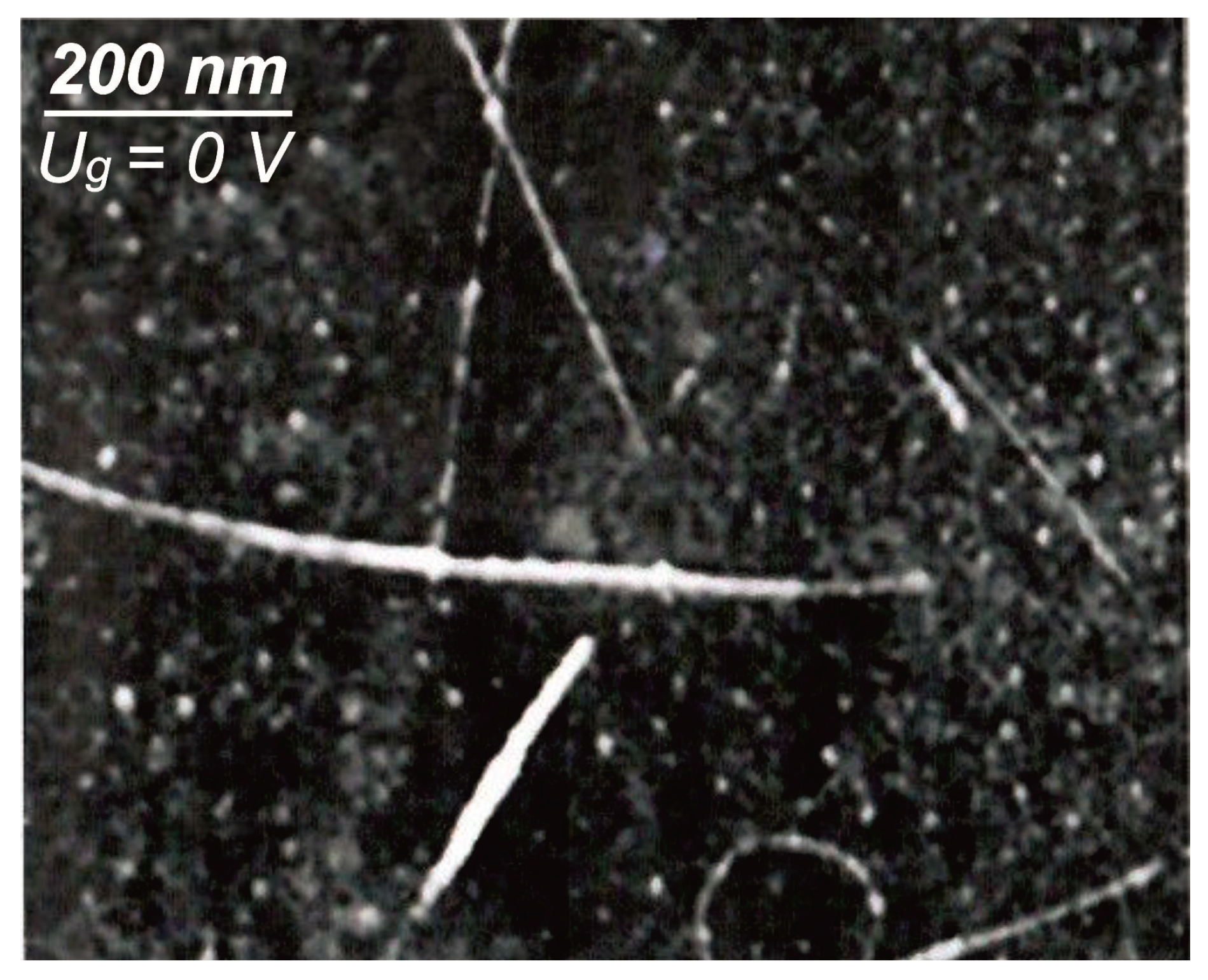
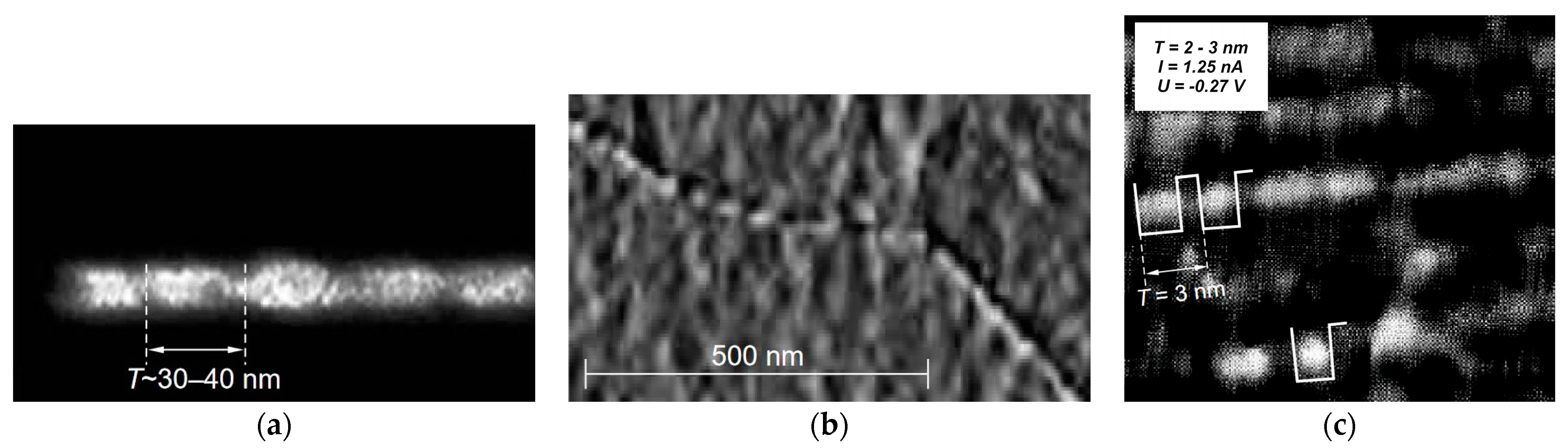
3.1. Experimental Studies of the Structure of CNTs
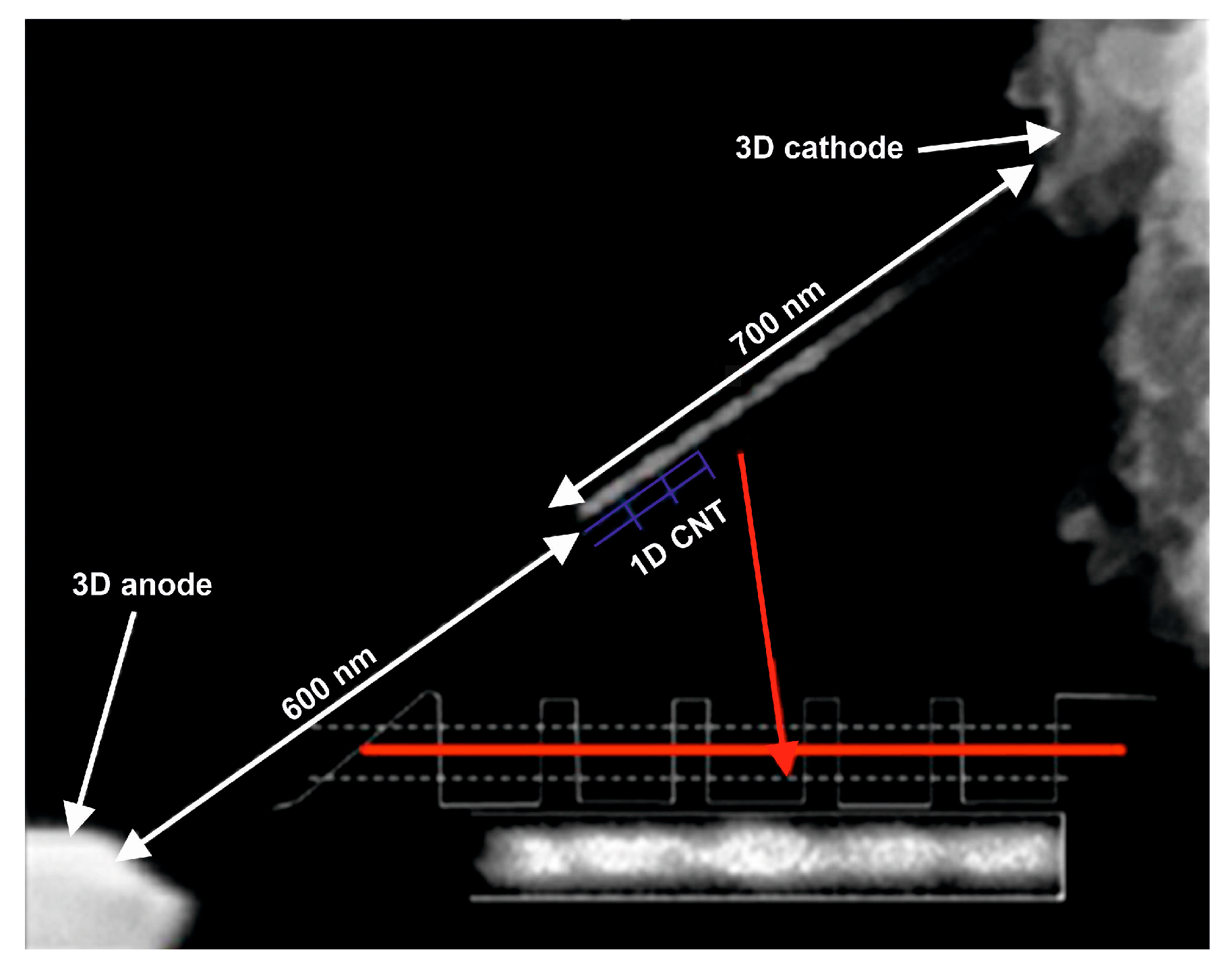
3.2. Experimental Studies of the Features of Charge Transfer in the Circuit of a Nanotube Emitter
4. Discussion
5. Conclusions
Author Contributions
Funding
Data Availability Statement
Conflicts of Interest
References
- Iijima, S. Helical microtubules of graphitic carbon. Nature 1991, 354, 56–58. [Google Scholar] [CrossRef]
- Kosakovskaya, Z.Y.; Chernozatonsky, L.A.; Fedorov, E.A. Nanofiber carbon structure. JETP Lett. 1992, 56, 26. [Google Scholar]
- Chernozatonskii, L.A. Barrelenes/tubelenes—A new class of cage carbon molecules and its solids. Phys. Lett. A 1992, 166, 55–60. [Google Scholar] [CrossRef]
- Bethune, D.S.; Kiang, C.H.; de Vries, M.S.; Gorman, G.; Savoy, R.; Vazquez, J.; Beyers, R. Cobalt-catalysed growth of carbon nanotubes with single-atomic-layer walls. Nature 1993, 363, 605–607. [Google Scholar] [CrossRef]
- Iijima, S.; Ichihashi, T. Single-shell carbon nanotubes of 1-nm diameter. Nature 1993, 363, 603–605. [Google Scholar] [CrossRef]
- Chernozatonskii, L.A.; Gulyaev, Y.V.; Kosakovskaja, Z.J.; Sinitsyn, N.I.; Torgashov, G.V.; Zakharchenko, Y.F.; Fedorov, E.A.; Val’chuk, V.P. Electron field emission from nanofilament carbon films. Chem. Phys. Lett. 1995, 233, 63–68. [Google Scholar] [CrossRef]
- Eletskii, A.V. Electron field emitters based on carbon nanotubes. Uspekhi Fiz. Nauk 2010, 180, 897–930. [Google Scholar] [CrossRef]
- Eidelman, E.D.; Arkhipov, A.V. Field emission from carbon nanostructures: Models and experiment. Phys.-Uspekhi 2020, 63, 648. [Google Scholar] [CrossRef]
- Cheng, Y.; Zhou, O. Electron field emission from carbon nanotubes. Comptes Rendus Phys. 2003, 4, 1021–1033. [Google Scholar] [CrossRef]
- Milne, W.I.; Teo, K.B.K.; Mann, M.; Bu, I.Y.Y.; Amaratunga, G.A.J.; de Jonge, N.; Allioux, M.; Oostveen, J.T.; Legagneux, P.; Minoux, E.; et al. Carbon nanotubes as electron sources. Phys. Status Solidi A 2006, 203, 1058–1063. [Google Scholar] [CrossRef]
- Lee, H.R.; Hwang, O.J.; Cho, B.; Park, K.C. Scanning electron imaging with vertically aligned carbon nanotube (CNT) based cold cathode electron beam (C-beam). Vacuum 2020, 182, 109696. [Google Scholar] [CrossRef]
- Wu, Z.; Xing, Y.; Ren, W.; Wang, Y.; Guo, H. Ballistic transport in bent-shaped carbon nanotubes. Carbon 2019, 149, 364–369. [Google Scholar] [CrossRef]
- Li, H.; Lu, W.G.; Li, J.J.; Bai, X.D.; Gu, C.Z. Multichannel ballistic transport in multiwall carbon nanotubes. Phys. Rev. Lett. 2005, 95, 086601. [Google Scholar] [CrossRef] [PubMed]
- Eletskii, A.V. Transport properties of carbon nanotubes. Phys.-Uspekhi 2009, 52, 209. [Google Scholar] [CrossRef]
- Zu, Y.; Yuan, X.; Xu, X.; Cole, M.T.; Zhang, Y.; Li, H.; Yin, Y.; Wang, B.; Yan, Y. Design and simulation of a multi-sheet beam terahertz radiation source based on carbon-nanotube cold cathode. Nanomaterials 2019, 9, 1768. [Google Scholar] [CrossRef] [PubMed]
- Milne, W.I.; Teo, K.B.K.; Amaratunga, G.A.J.; Legagneux, P.; Gangloff, L.; Schnell, J.-P.; Semet, V.; Binh, V.T.; Groening, O. Carbon nanotubes as field emission sources. J. Mater. Chem. 2004, 14, 933–943. [Google Scholar] [CrossRef]
- Zou, R.; Hu, J.; Song, Y.; Wang, N.; Chen, H.; Chen, H.; Chen, Z. Carbon nanotubes as field emitter. J. Nanosci. Nanotechnol. 2010, 10, 7876–7896. [Google Scholar] [CrossRef]
- Xu, X.; Yuan, X.; Chen, Q.; Cole, M.T.; Zhang, Y.; Xie, J.; Yin, Y.; Li, H.; Yan, Y. A low-voltage, premodulation terahertz oscillator based on a carbon nanotube cold cathode. IEEE Trans. Electron Devices 2020, 67, 1266–1269. [Google Scholar] [CrossRef]
- Gu, Y.; Yuan, X.; Xu, X.; Cole, M.; Chen, Q.; Zhang, Y.; Wang, B.; Li, H.; Yin, Y.; Yan, Y. A high-current-density terahertz electron-optical system based on carbon nanotube cold cathode. IEEE Trans. Electron Devices 2020, 67, 5760–5765. [Google Scholar] [CrossRef]
- Huo, C.; Liang, F.; Sun, A.B. Review on development of carbon nanotube field emission cathode for space propulsion systems. High Volt. 2020, 5, 409–415. [Google Scholar] [CrossRef]
- Tang, Y.; Amlani, I.; Orlov, A.O.; Snider, G.L.; Fay, P.J. Operation of single-walled carbon nanotube as a radio-frequency single-electron transistor. Nanotechnology 2007, 18, 445203. [Google Scholar] [CrossRef]
- Soldatov, E.S.; Kolesov, V.V. The single electronics: Past, present, future. RENSIT 2012, 4, 71–90e. [Google Scholar]
- Wang, A.; Zhao, J.; Chen, K.; Li, Z.; Li, C.; Dai, Q. Ultra Coherent Single Electron Emission of Carbon Nanotubes. Adv. Mater. Adv. Mater. 2023, 35, 2300185. [Google Scholar] [CrossRef] [PubMed]
- Sugie, H.; Tanemura, M.; Filip, V.; Iwata, K.; Takahashi, K.; Okuyama, F. Carbon nanotubes as electron source in an x-ray tube. Appl. Phys. Lett. 2001, 78, 2578–2580. [Google Scholar] [CrossRef]
- Musatov, A.L.; Gulyaev, Y.V.; Izrael’yants, K.R.; Kukovitskii, E.F.; Kiselev, N.A.; Maslennikov, O.Y.; Guzilov, I.A.; Ormont, A.B.; Chirkova, E.G. A compact X-ray tube with a field emitter based on carbon nanotubes. J. Commun. Technol. Electron. 2007, 52, 714–716. [Google Scholar] [CrossRef]
- Parmee, R.J.; Collins, C.M.; Milne, W.I.; Cole, M.T. X-ray generation using carbon nanotubes. Nano Converg. 2015, 2, 1. [Google Scholar] [CrossRef]
- Psuja, P.; Hreniak, D.; Strek, W. The concept of a new simple low-voltage cathodoluminescence set-up with CNT field emission cathodes. In Proceedings of the Reliability, Packaging, Testing, and Characterization of MEMS/MOEMS and Nanodevices VIII, San Jose, CA, USA, 28–29 January 2009; Volume 7206, pp. 132–137. [Google Scholar]
- Wilson, N.R.; Macpherson, J.V. Carbon nanotube tips for atomic force microscopy. Nat. Nanotechnol. 2009, 4, 483–491. [Google Scholar] [CrossRef]
- Shingaya, Y.; Nakayama, T.; Aono, M. Carbon nanotube tip for scanning tunneling microscopy. Phys. B Condens. Matter 2002, 323, 153–155. [Google Scholar] [CrossRef]
- Clauss, W. Scanning tunneling microscopy of carbon nanotubes. Appl. Phys. A 1999, 69, 275–281. [Google Scholar] [CrossRef]
- Biró, L.P.; Thiry, P.A.; Lambin, P.; Journet, C.; Bernier, P.; Lucas, A.A. Influence of tunneling voltage on the imaging of carbon nanotube rafts by scanning tunneling microscopy. Appl. Phys. Lett. 1998, 73, 3680–3682. [Google Scholar] [CrossRef]
- Dai, H.; Hafner, J.H.; Rinzler, A.G.; Colbert, D.T.; Smalley, R.E. Nanotubes as nanoprobes in scanning probe microscopy. Nature 1996, 384, 147–150. [Google Scholar] [CrossRef]
- Kim, S.J. Vacuum gauges with emitters based on carbon nanotubes. Tech. Phys. Lett. 2005, 31, 597–599. [Google Scholar] [CrossRef]
- Fowler, R.H.; Nordheim, L. Electron emission in intense electric fields. Proceedings of the Royal Society of London. Ser. A Contain. Pap. A Math. Phys. Character 1928, 119, 173–181. [Google Scholar]
- Forbes, R.G. Field emission: New theory for the derivation of emission area from a Fowler–Nordheim plot. J. Vac. Sci. Technol. B Microelectron. Nanometer Struct. Process. Meas. Phenom. 1999, 17, 526–533. [Google Scholar] [CrossRef]
- Liang, S.-D.; Chen, L. Generalized fowler-nordheim theory of field emission of carbon nanotubes. Phys. Rev. Lett. 2008, 101, 027602. [Google Scholar] [CrossRef]
- Jensen, K.L. Electron emission theory and its application: Fowler–Nordheim equation and beyond. J. Vac. Sci. Technol. B: Microelectron. Nanometer Struct. Process. Meas. Phenom. 2003, 21, 1528–1544. [Google Scholar] [CrossRef]
- Lepetit, B. Electronic field emission models beyond the Fowler-Nordheim one. J. Appl. Phys. 2017, 122, 215105. [Google Scholar] [CrossRef]
- Vul’, A.; Reich, K.; Eidelman, E.; Terranova, M.L.; Ciorba, A.; Orlanducci, S.; Sessa, V.; Rossi, M. A Model of Field Emission from Carbon Nanotubes Decorated by Nanodiamonds. Adv. Sci. Lett. 2010, 3, 110–116. [Google Scholar] [CrossRef]
- Katkov, V.L.; Osipov, V.A. Energy distributions of field emitted electrons from carbon nanosheets: Manifestation of the quantum size effect. JETP Lett. 2009, 90, 278–283. [Google Scholar] [CrossRef]
- Xie, S.S.; Li, W.Z.; Qian, L.X.; Chang, B.H.; Fu, C.S.; Zhao, R.A.; Zhou, W.Y.; Wang, G. Equilibrium shape equation and possible shapes of carbon nanotubes. Phys. Rev. B 1996, 54, 16436. [Google Scholar] [CrossRef]
- Fursey, G.N. Field Emission in Vacuum Micro-Electronics; Kluwer Academic/Plenum Publishers: New York, NY, USA; Springer: Berlin/Heidelberg, Germany, 2005; p. 205. [Google Scholar]
- Yafyasov, A.; Bogevolnov, V.; Fursey, G.; Pavlov, B.; Polyakov, M.; Ibragimov, A. Low-threshold emission from carbon nano-structures. Ultramicroscopy 2011, 111, 409–414. [Google Scholar] [CrossRef] [PubMed]
- Yafyasov, A.; Bogevolnov, V.; Fursey, G.; Pavlov, B.; Polyakov, M.; Ibragimov, A.; Fursei, G.N.; Polyakov, M.A.; Kantonistov, A.A. Field and explosive emissions from graphene-like structures. Tech. Phys. 2013, 58, 845–851. [Google Scholar]
- Kleshch, V.I.; Porshyn, V.; Serbun, P.; Orekhov, A.S.; Ismagilov, R.R.; Malykhin, S.A.; Eremina, V.A.; Obraztsov, P.A.; Obraztsova, E.D.; Lützenkirchen-Hecht, D. Coulomb blockade in field electron emission from carbon nanotubes. Appl. Phys. Lett. 2021, 118, 053101. [Google Scholar] [CrossRef]
- Pascale-Hamri, A.; Perisanu, S.; Derouet, A.; Journet, C.; Vincent, P.; Ayari, A.; Purcell, S.T. Ultrashort single-wall carbon nanotubes reveal field-emission coulomb blockade and highest electron-source brightness. Phys. Rev. Lett. 2014, 112, 126805. [Google Scholar] [CrossRef] [PubMed]
- Padya, B.; Ravi, M.; Jain, P. Growth and integration of aligned carbon nanotube-based field emission cathode for electron gun device-level fabrication. Nano Trends 2023, 2, 100009. [Google Scholar] [CrossRef]
- DI Bartolomeo, A.; Scarfato, A.; Giubileo, F.; Bobba, F.; Biasiucci, M.; Cucolo, A.M.; Santucci, S.; Passacantando, M. A local field emission study of partially aligned carbon-nanotubes by atomic force microscope probe. Carbon N. Y. 2007, 45, 2957–2971. [Google Scholar] [CrossRef]
- Giubileo, F.; Di Bartolomeo, A.; Scarfato, A.; Iemmo, L.; Bobba, F.; Passacantando, M.; Santucci, S.; Cucolo, A. Local probing of the field emission stability of vertically aligned multi-walled carbon nanotubes. Carbon N. Y. 2009, 47, 1074–1080. [Google Scholar] [CrossRef]
- Kibis, O.V.; Parfitt, D.G.W.; Portnoi, M.E. Superlattice properties of carbon nanotubes in a transverse electric field. Phys. Rev. B 2005, 71, 035411. [Google Scholar] [CrossRef]
- Ayuela, A.; Chico, L.; Jaskólski, W. Electronic band structure of carbon nanotube superlattices from first-principles calculations. Phys. Rev. B 2008, 77, 085435. [Google Scholar] [CrossRef]
- Shokri, A.A.; Khoeini, F. Electron localization in superlattice-carbon nanotubes. Eur. Phys. J. B 2010, 78, 59–64. [Google Scholar] [CrossRef]
- Wilder, J.W.; Venema, L.C.; Rinzler, A.G.; Smalley, R.E.; Dekker, C. Electronic structure of atomically resolved carbon nanotubes. Nature 1998, 391, 59–62. [Google Scholar] [CrossRef]
- Zhang, J.; Liu, S.; Nshimiyimana, J.P.; Deng, Y.; Hu, X.; Chi, X.; Wu, P.; Liu, J.L.; Chu, W.; Sun, L. Observation of van Hove singularities and temperature dependence of electrical characteristics in suspended carbon nanotube Schottky barrier transistors. Nano-Micro Lett. 2018, 10, 25. [Google Scholar] [CrossRef] [PubMed]
- Yang, Y.; Fedorov, G.; Shafranjuk, S.E.; Klapwijk, T.M.; Cooper, B.K.; Lewis, R.M.; Lobb, C.J.; Barbara, P. Electronic transport and possible superconductivity at van hove singularities in carbon nanotubes. Nano Lett. 2015, 15, 7859–7866. [Google Scholar] [CrossRef]
- Jaskólski, W.; Stachow, A.; Chico, L. Band structure and quantum conductance of metallic carbon nanotube superlattices. Acta Phys. Pol.-Ser. A Gen. Phys. 2005, 108, 697–704. [Google Scholar] [CrossRef]
- Kim, P.; Odom, T.W.; Huang, J.L.; Lieber, C.M. Electronic density of states of atomically resolved single-walled carbon nanotubes: Van Hove singularities and end states. Phys. Rev. Lett. 1999, 82, 1225. [Google Scholar] [CrossRef]
- Lieber, C.M. Nanowire superlattices. Nano Lett. 2002, 2, 81–82. [Google Scholar] [CrossRef]
- Lambin, P.; Loiseau, A.; Culot, C.; Biro, L.P. Structure of carbon nanotubes probed by local and global probes. Carbon 2002, 40, 1635–1648. [Google Scholar] [CrossRef]
- Grishin, M.V.; Dadidchik, F.I.; Kovalevsky, S.A. Ordered adsorption of carbon nanotubes on pyrolytic graphite Surface. X-Ray Synchrotron Neutron Res. 2001, 7, 103. Available online: http://www.issp.ac.ru/journal/surface/2001/07-2001.htm?ysclid=lpr5mrjes71202709 (accessed on 14 July 2023). (In Russian).
- Dalidchik, F.I.; Grishin, M.V.; Kovalevsky, S.A. Features of the electronic structure of interacting nanocarbon particles. Microsyst. Eng. 2004, 7, 29–33. Available online: https://elibrary.ru/download/elibrary_9497233_15437905.pdf (accessed on 14 July 2023). (In Russian).
- Dalidchik, F.I.; Balashov, E.M.; Grishin, M.V. Scanning tunneling spectroscopy of interacting nanocarbon sp2 structures. Russ. Chem. J. 2005, 159, 98–104. [Google Scholar]
- Dalidchik, F.I.; Shub, B.R. Scanning tunneling microscopy and spectroscopy of imperfect and interacting nanoparticles (metal oxides and carbon). Russ. Nanotechnol. 2006, 1, 82–96. (In Russian) [Google Scholar]
- Bonard, J.M.; Dean, K.A.; Coll, B.F.; Klinke, C. Field emission of individual carbon nanotubes in the scanning electron microscope. Phys. Rev. Lett. 2002, 89, 197602. [Google Scholar] [CrossRef]
- Bonard, J.M.; Salvetat, J.P.; Stöckli, T.; Forro, L.; Chatelain, A. Field emission from carbon nanotubes: Perspectives for applications and clues to the emission mechanism. Appl. Phys. A 1999, 69, 245–254. [Google Scholar] [CrossRef]
- Bower, C.; Zhu, W.; Shalom, D.; Lopez, D.; Chen, L.H.; Gammel, P.L.; Jin, S. On-chip vacuum microtriode using carbon nanotube field emitters. Appl. Phys. Lett. 2002, 80, 3820–3822. [Google Scholar] [CrossRef]
- Manohara, H.; Dang, W.L.; Siegel, P.H.; Hoenk, M.; Husain, A.; Scherer, A. Field emission testing of carbon nanotubes for THz frequency vacuum microtube sources. In Proceedings of the Reliability, Testing, and Characterization of MEMS/MOEMS III, San Jose, CA, USA, 27–29 January 2003; Volume 5343, pp. 227–234. [Google Scholar]


Disclaimer/Publisher’s Note: The statements, opinions and data contained in all publications are solely those of the individual author(s) and contributor(s) and not of MDPI and/or the editor(s). MDPI and/or the editor(s) disclaim responsibility for any injury to people or property resulting from any ideas, methods, instructions or products referred to in the content. |
© 2023 by the authors. Licensee MDPI, Basel, Switzerland. This article is an open access article distributed under the terms and conditions of the Creative Commons Attribution (CC BY) license (https://creativecommons.org/licenses/by/4.0/).
Share and Cite
von Gratowski, S.V.; Kosakovskaya, Z.Y.; Koledov, V.V.; Shavrov, V.G.; Smolovich, A.M.; Orlov, A.P.; Denisjuk, R.N.; Wang, C.; Liang, J. Structural Inhomogeneities and Nonlinear Phenomena in Charge Transfer under Cold Field Emission in Individual Closed Carbon Nanotubes. Micro 2023, 3, 941-954. https://doi.org/10.3390/micro3040064
von Gratowski SV, Kosakovskaya ZY, Koledov VV, Shavrov VG, Smolovich AM, Orlov AP, Denisjuk RN, Wang C, Liang J. Structural Inhomogeneities and Nonlinear Phenomena in Charge Transfer under Cold Field Emission in Individual Closed Carbon Nanotubes. Micro. 2023; 3(4):941-954. https://doi.org/10.3390/micro3040064
Chicago/Turabian Stylevon Gratowski, S. V., Z. Ya. Kosakovskaya, V. V. Koledov, V. G. Shavrov, A. M. Smolovich, A. P. Orlov, R. N. Denisjuk, Cong Wang, and Junge Liang. 2023. "Structural Inhomogeneities and Nonlinear Phenomena in Charge Transfer under Cold Field Emission in Individual Closed Carbon Nanotubes" Micro 3, no. 4: 941-954. https://doi.org/10.3390/micro3040064