1. Introduction
The manufacturing of power devices and their utilization in many applications, such as electric vehicles, power grids, and railway traction, are going through a phase in which SiC power MOSFETs are replacing their conventional silicon counterparts. Indeed, SiC devices have the advantage of better performance regarding higher blocking voltage, higher operating temperature and higher operating frequency [
1]. The reliability of SiC power MOSFETs is a critical issue and atmospheric neutrons are a concern among the several failure and degradation mechanisms. The neutron failures are important in both avionic [
2] and terrestrial [
3] applications.
The interaction between atmospheric neutrons and power MOSFETs operating at high voltages may cause catastrophic single-event burnout (SEB) failure. Compared to Si power devices, SiC devices are less sensitive to SEB failure induced by neutrons [
4,
5,
6], although a higher derating factor is needed for SiC devices with higher blocking voltages [
7]. The hazard to SEB failure is quantified by the failure in time (FIT) parameter. Due to the low flux of terrestrial neutrons (≈25 neutrons·cm
for energies higher than 1 MeV at sea level [
8]), accelerated neutron tests are needed to determine the FIT values of the power devices under different operating conditions [
5,
6,
9,
10]. The accelerated neutron tests are usually performed at fixed drain bias voltage and with the devices held at room temperature.
Concerning investigations of the SEB temperature susceptibility due to high-energy neutrons, it is useful to determine more accurately the FIT of the devices during their real operating conditions in power systems, according to a specific mission profile (function of the operating conditions: voltage, temperature, altitude, etc.). For example, SiC devices can operate with a junction temperature over 220 °C [
11]. Conversely, knowledge of the trend of the FIT parameter at low temperatures can be useful for both avionic and automotive applications.
Only a few studies on FIT data for power MOSFETs at different temperatures are present in the literature [
12,
13,
14]. Generally, for both Si and SiC MOSFETs, the FIT parameter decreases as the temperature increases, although in [
14] a slightly higher failure rate at high temperatures for SiC power MOSFETs was observed.
An empirical formula reported in [
15], valid for Si devices, predicts an exponential decreasing of the failure rate with increasing temperature. This trend was observed in [
12] for Super-Junction Si MOSFET. The exponential dependence of the FIT on the temperature observed in Si devices does not hold for SiC power MOSFETs, which showed a weaker temperature dependence, as observed in [
14].
The FIT rate of different configurations of 3.3 kV and 6.5 kV SiC full-power modules under several operating conditions were calculated in [
16]. The temperature dependence of the FIT is estimated by assuming that this dependence is governed by the temperature dependence of the avalanche voltage
. The correlation between the FIT of SiC power devices assessed by neutron irradiation and the multiplication factor measured by radioactive sources was demonstrated in [
17]. The same authors characterized the multiplication factor of Si and SiC power devices at liquid nitrogen and ambient temperatures by using soft-gamma radioactive sources [
18]. They observed that the curves of the multiplication coefficient versus the ratio
at liquid nitrogen and ambient temperatures are almost superimposed. Based on this result, they concluded that the multiplication factor as a function of the normalized bias
, obeys a universal law, similarly to what has been proposed in the literature for the FIT of SiC power MOSFETs [
4]. From the above information, it emerges that in most cases the study of the temperature effects on the SEB failure of SiC devices was conducted via simulations or measurements of the impact ionization coefficient by using ionizing radiation or particles other than neutrons.
In this work, we present the results of neutron FIT data of SiC MOSFETs at different temperatures and bias voltages. We tested in the −50 °C–180 °C temperature range, one Si MOSFET and SiC MOSFETs with different technologies. The use of a large amount of failed samples allowed us to determine the FIT values with good precision. Moreover, to the best of our knowledge, this work represents the first time that FIT data of SiC power MOSFETs were presented at temperatures below room temperature.
In order to correlate the FIT versus temperature curves with the temperature dependence of the avalanche voltage, we measured the avalanche voltage as a function of the temperature.
Finally, preliminary results are presented concerning the measurement of the deposited charge in the power MOSFETs induced by neutrons at different temperatures by employing the MOSFET as a neutron detector.
3. Results
The results of the destructive tests of the power MOSFETs were performed at different values of temperature and drain bias voltage
, with
. The following graphs show the FIT values at sea level and their 95% confidence intervals (CI). The FIT value and its confidence interval are calculated according to the following formulas [
21]:
where
r is the number of failures of devices,
, where
is the neutron fluence to fail of the
i-th device,
(neutrons/cm
) is neutron fluence at sea level/New York City in
device−hours and
is the
u percentile of the chi-square distribution with
r degrees of freedom.
5% for 95% confidence.
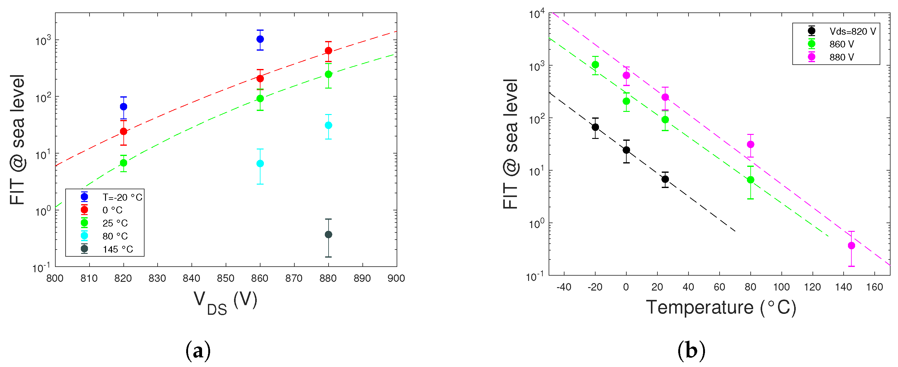
Figure 3 shows the FIT values of the Si VJNL MOSFET versus the bias drain voltage at different temperatures (
Figure 3a) and FIT versus temperature at some fixed
voltages (
Figure 3b).
We note that the FIT depends exponentially on the temperature and the drain bias voltage according to the phenomenological model given in [
15]. The dashed lines shown in these Figures are the best fits of this model, which allows calculating the failure rate as a function of blocking voltage and junction temperature.
For the Si BQ65 MOSFET, we have measured the FIT value only at room temperature, obtaining the value 53, with [34, 76] 95% CI, at
= 450 V. The investigations on the temperature effects were performed for this device only for the avalanche voltage.
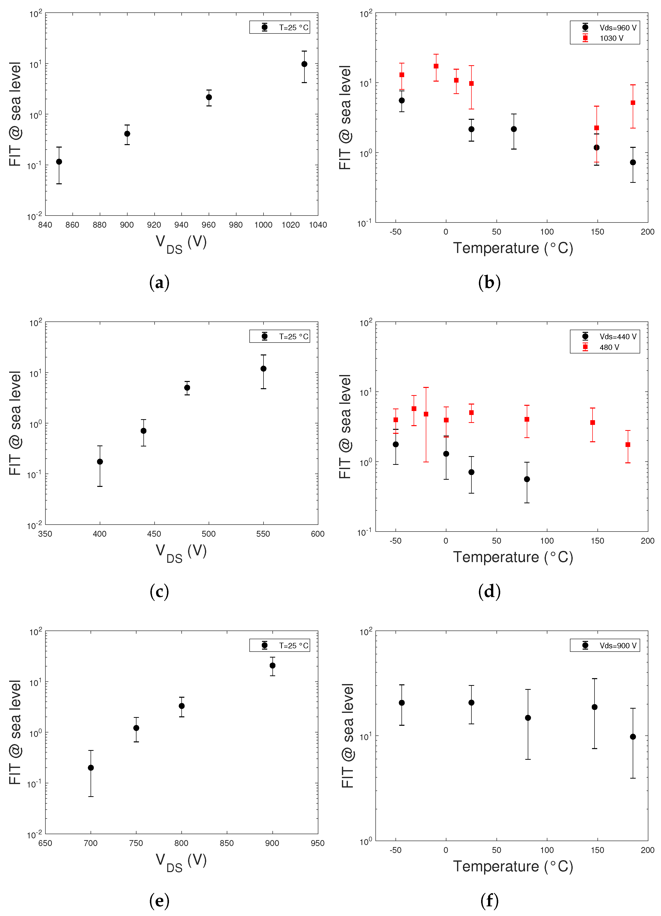
Figure 4a,c,e show the FIT versus the drain bias curves, at
T = 25 °C, of the SiC MOSFETs SQKW, SQF9 and BRJRL, respectively.
Figure 4b,d show the FIT versus temperature curves of the SiC SQKW and SQF9, respectively, at two different bias drain voltages.
Figure 4f shows the FIT versus temperature curve at fixed
voltage of the BRJRL device.
We note that the FIT values of the SiC power MOSFETs have a less marked dependence on both voltage and temperature, with respect to those of the Si device. The FIT increases exponentially with increases in the , but at a rate smaller than that of the Si device. Concerning the temperature dependence at fixed voltage, the FIT trend with the temperature is not marked and seems to depend on the drain bias voltage. For example, for the SQF9 SiC MOSFET, at V the FIT decreases with the temperature increasing, whereas at 480 V the FIT is almost constant with temperature.
The FIT-temperature curves of the SiC SQKW show that the FIT values at V and at 1030 V seem to decrease when the temperature increases, although at 1030 V this trend is less marked than that at 960 V.
3.1. Weibull Analysis
From the results of the FIT data of the SiC devices, a clear trend with the temperature of the FIT values does not emerge. For example, the FIT versus temperature curves of the SQF9 show a FIT trend with temperature at V, whereas at V the FIT seems to not depend on the temperature. This ambiguity arises from the large width of the confidence interval bars of the FIT values, due to the low amount of failed devices at each temperature. To mitigate this uncertainty, for each device at fixed drain voltage, we calculate the Weibull distributions of the neutron fluence to fail in the following two cases:
It is known that the physical mechanism for neutron-induced failure in power electronic devices stipulates a constant failure rate corresponding to Weibull distribution of the neutron fluence to fail with shape parameter . When there is a significant FIT temperature dependence, the estimated shape parameter of the Weibull distribution of the failed devices at the merged temperatures must be lower than 1. Hence, to detect the effects of the temperature, we estimated for each device the distribution F at °C and at different temperatures. From the F data, we estimate with the maximum likelihood method the shape parameter and its 95% confidence interval.
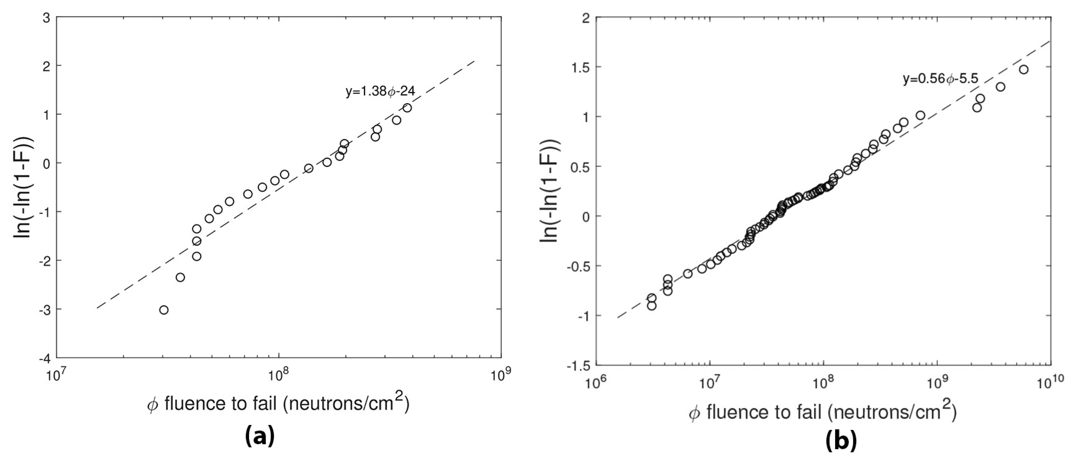
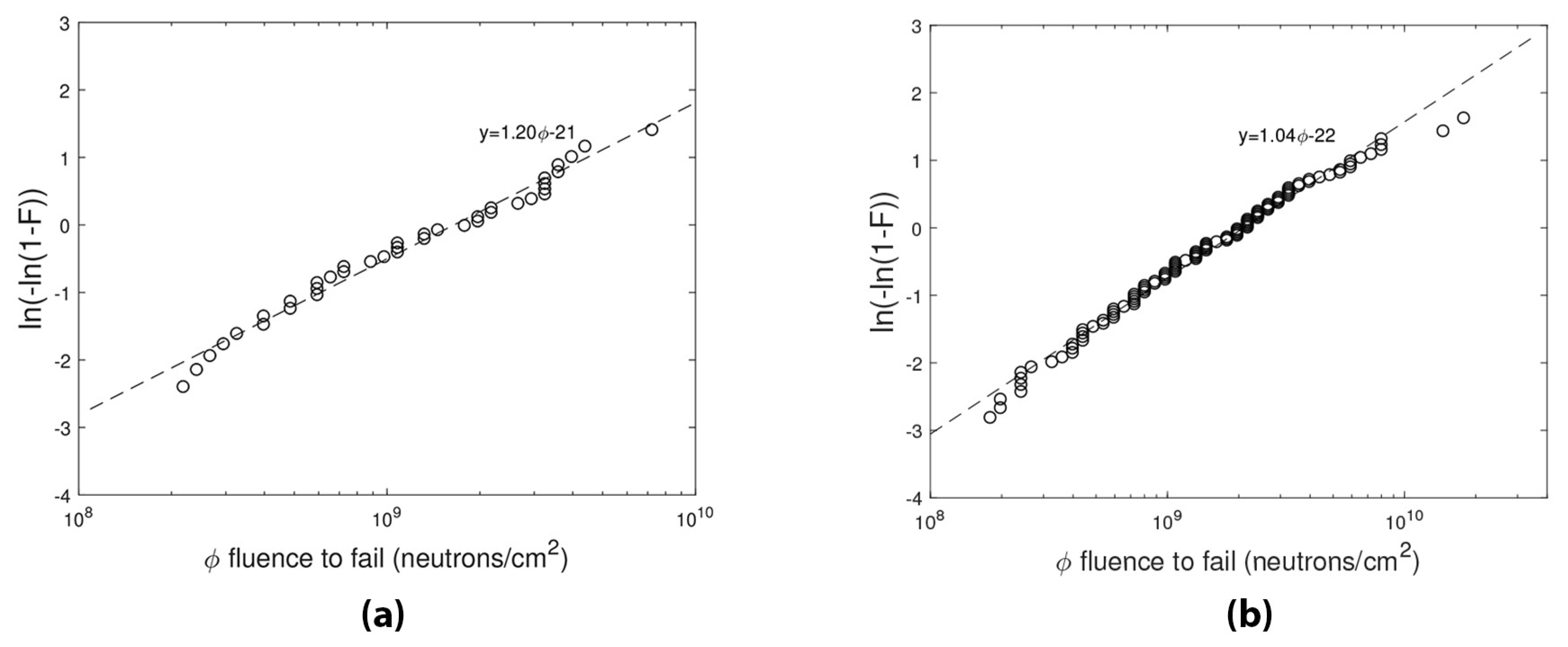
Figure 5 shows the Weibull plots of the Si VJNL, at
°C (
Figure 5a) and at the merged temperatures (
Figure 5b).
Figure 6 shows the Weibull plots of the SiC SQF9 MOSFET.
Table 2 lists the values of
of the Weibull distributions at room temperature and with the merged temperatures. For each device, at a fixed drain voltage value, the Weibull distribution and its shape parameter was estimated from the failed devices at
°C and those at all temperatures. We observe that for the Si VJNL a significant reduction of the
occurs in the
F distribution of the data at all temperatures. This confirms the marked trend with the temperature of the failure rate.
We apply this method to the SiC MOSFETs and the results, summarized in
Table 2, show that for the SQF9 at
V and the BRJRL at
V the FIT is not affected by the temperature, whereas the FIT of the SQKW at 960 V depends on the temperature.
For the SQF9 at V and the SQKW at 1030 V, the Weibull analysis is precluded due to the lack of sufficient failed samples.
3.2. Avalanche Voltage versus Temperature
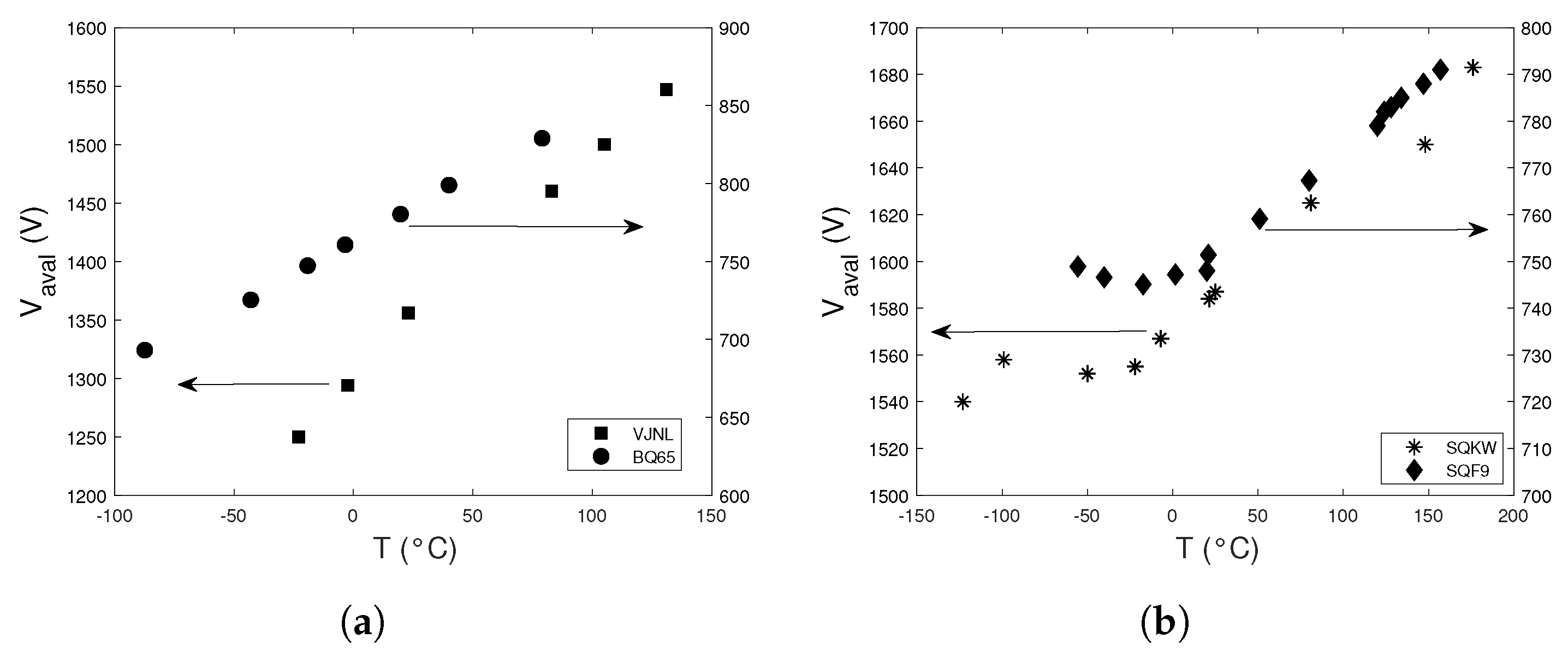
Figure 7 shows the measured avalanche voltage
versus the temperature
T for the BQ65 and VJNL Si power MOSFETs (
Figure 7a) and for the SQF9 and SQKW SiC devices.
For Si devices, the avalanche voltage monotonically increases with increasing temperature, ≈1 V/°C for the BQ65 and ≈2 V/°C for the VJNL. For SiC power MOSFETs, the avalanche voltage is almost constant in the low temperature range, up to ≈25 °C, and then increases with the temperature increasing with a rate of ≈0.3 V/°C for the SQF9 and ≈0.6 V/°C for the SQKW device.
3.3. Waveforms Analysis of the MOSFET Working as a Detector under Neutron Irradiation
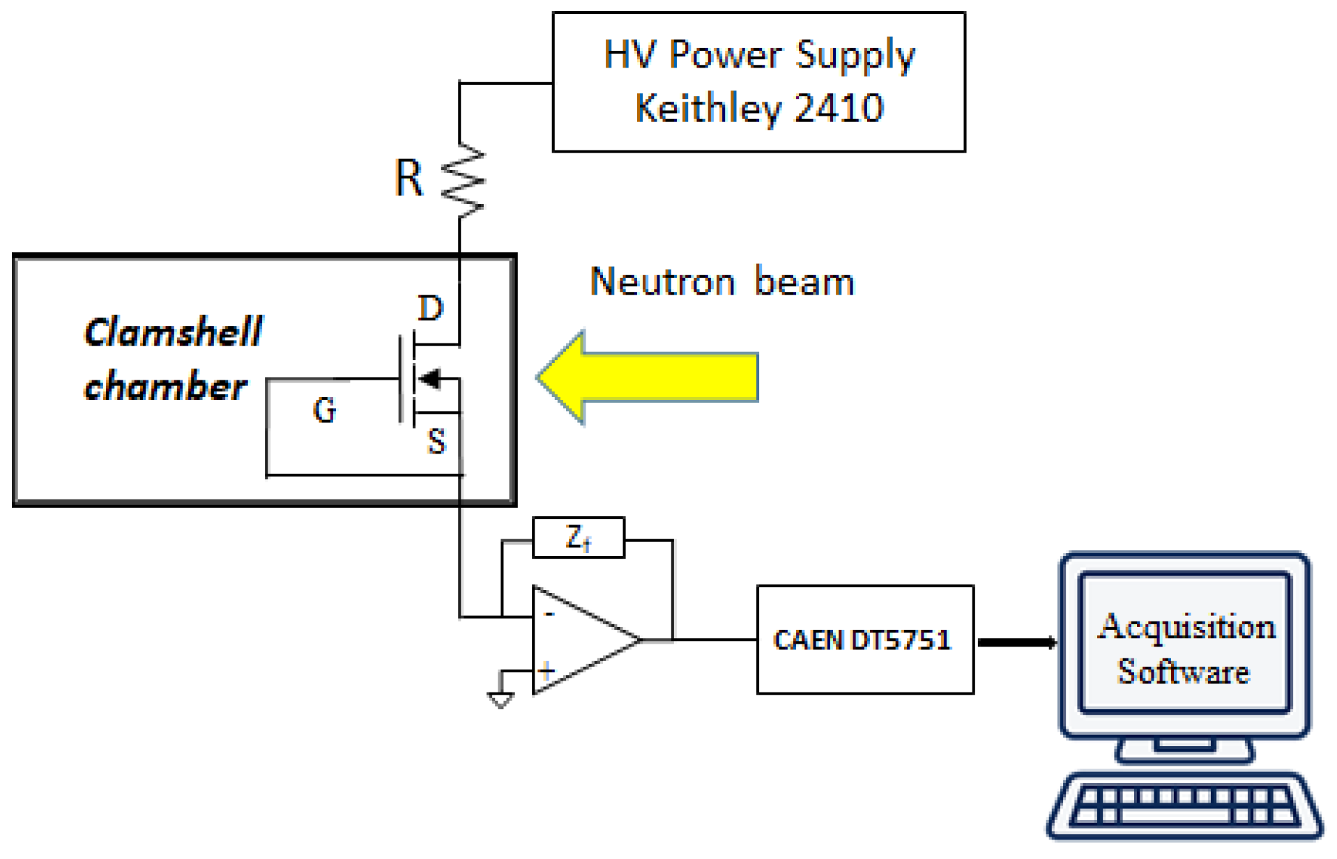
Regarding the setup to detect the current pulses of the MOSFET under neutron irradiation, we performed irradiation runs with the Si VJNL MOSFETs and with the SiC SQKW devices. For each irradiation run, the device was biased at fixed
value.
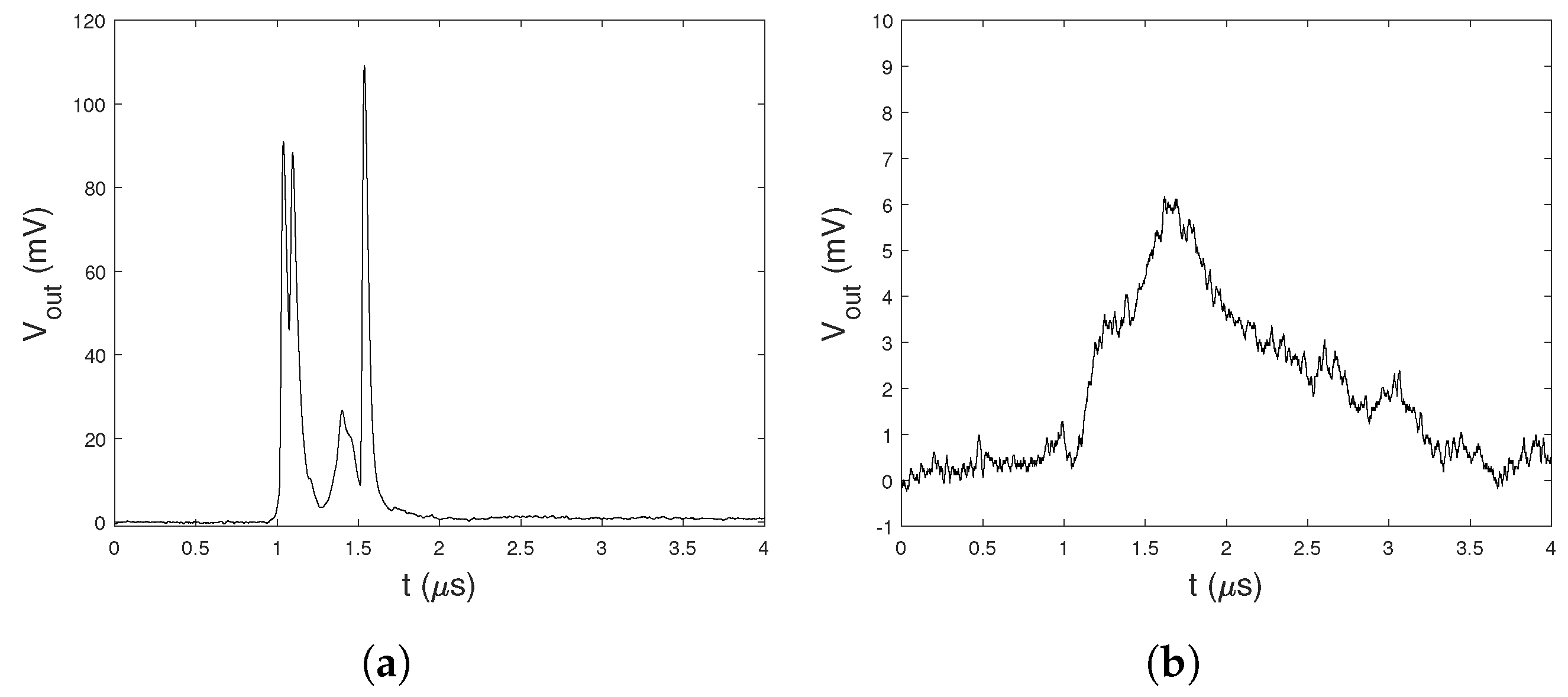
Figure 8 shows the acquired waveforms of the TIA output due to a single neutron burst, for the Si VJNL
Figure 8a and SiC SQKW
Figure 8b devices at
°C.
Although the resistor R between the drain and power supply was 6.8 M for the VJNL and 4700 for SQKW, the amplitude of the current signals of the Si device are greater than those of the SiC device. This could be explained by the higher ratio and by the greater sensitive region of the VJNL with respect to those of the SQKW.
In the case of the VJNL waveforms shown in
Figure 8a, can be distinguished two pulses due to the two neutron bunches, the first begins at
μs and the second at
μs. These signals are ≈300 ns apart. This value is close to the mean value of the time delay of 360 ns between the two neutron bunches provided by the neutron source. In other cases, more than two pulses per bunch are present. For the SiC SQKW MOSFET, is not possible to clearly distinguish two or more pulses per each neutron burst.
Temperature Effects on the Deposited Charge
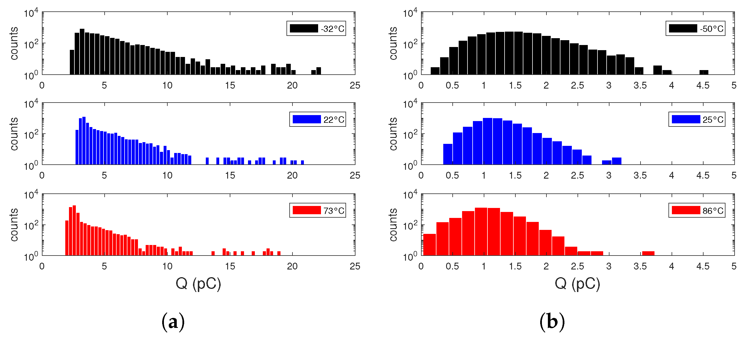
To investigate the temperature effects on the MOSFETs waveforms induced by the neutrons, we performed, for each device, several acquisitions at fixed drain voltage and three different temperatures: one temperature close to the room value, one lower and the other higher. For each acquired waveform we calculate the deposited charge Q by numerical integration of drain current due to a single neutron burst, although during one neutron burst more current pulses are present and the deposited charge per each pulse should be calculated.
Figure 9 shows the histograms of the deposited charge
Q for the VJNL
Figure 9a and SQKW
Figure 9b at different temperatures. The number of neutron burst
is 5000 for both devices and for each temperature.
We observe that for both devices as the temperature increases, the counts at higher values of Q decrease. The deposited charge in the VJNL is almost one order of magnitude greater than that of the SiC device. Moreover, in the VJNL are present overflow pulses which exceed the input range of the digitizer. These pulses were excluded in the calculation of the deposited charge. The number of overflow pulses increases as the temperature decreases. Indeed, these overflow pulses are 4.8% at T = −32 °C, 2.0% at T = 22 °C and 0.3% at T = 73 °C of the whole neutron bursts. These overflow pulses were not observed in the SiC device.
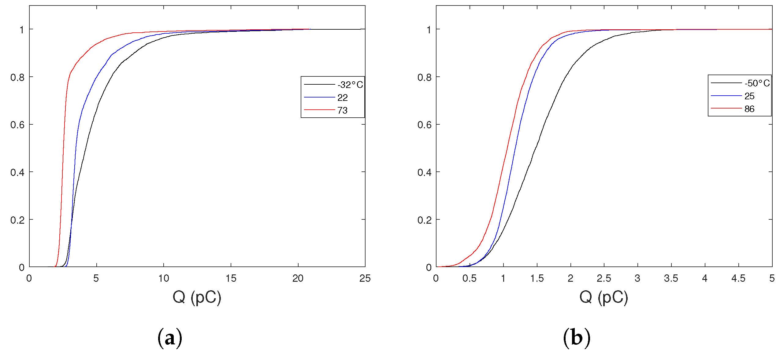
To better highlight the temperature effects on
Q,
Figure 10 shows the empirical cumulative distribution functions (CDF) of
Q for the VJNL
Figure 10a and SQKW
Figure 10b.
We note that the CDFs shift toward higher Q values as the temperature decreases. Hence, we conclude that temperature modifies the amount of charge produced inside the sensitive region by neutron interaction for both silicon and silicon carbide MOSFETs.
4. Discussion
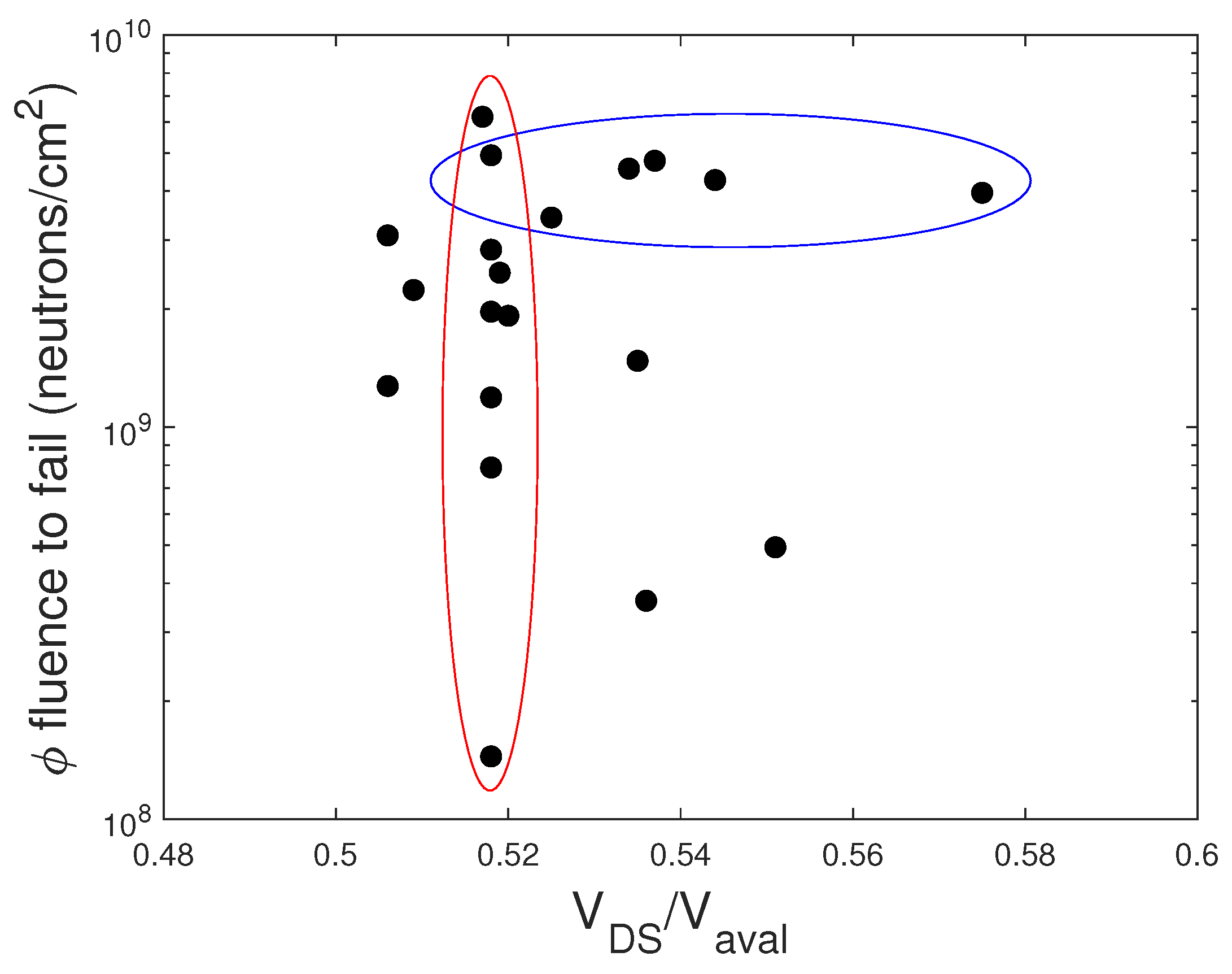
From the results of our experiments emerge a clear behavior of temperature dependence of the FIT for the silicon power MOSFET, which corroborates current data presented in the literature. The failure rate due to the SEB induced by fast and ultra-fast neutrons depends exponentially on both the temperature and drain bias voltage. This temperature dependence was also confirmed by the proposed Weibull analysis. In this work, the silicon devices were used as golden sample to validate our methods used to investigate the temperature effects on the neutron-induced SEB in SiC power MOSFETs, for which the FIT results do not show a clear trend with the temperature.
With the known temperature dependence of the avalanche voltage
, the FIT versus
curves could explain FIT temperature dependence in SiC MOSFETs as proposed in [
16,
18]. This analysis applied to the FIT data would be cumbersome because the values of the avalanche voltage exhibit a large spread as well as their temperature drift. As an example,
Figure 11 shows the neutron fluence to fail versus the
of the BRJRL at
T = 25 °C and
V. Despite the small sample size, we note the large spread of the
values and the lack of correlation between the avalanche voltage and the neutron fluence to fail. This lack of correlation has been already observed in [
6] for different SiC power MOSFETs. In particular, as represented by the blue and red circles in
Figure 11, some devices (blue circle) fail at almost the same neutron fluence but at different values of
. The other batch (red circle) with the same
value fail at neutron fluences which differ over one order of magnitude.
Concerning the temperature dependence at fixed drain voltage of the FIT values of the SiC power MOSFETs, the results of our investigation confirmed the lower temperature dependence of the silicon power MOSFETs and showed that the FIT-temperature curves depend on the SiC device and its bias condition.
Some physical mechanisms governing the temperature dependence of the SEB failures have been proposed in [
12] for Si MOSFETs and in [
14] for SiC MOSFETs. For silicon devices, the SEB mechanism is due to the parasitic bipolar transistor turn-on due to the dense electron-hole plasma produced by an ion which traverses the depletion region of the n-channel MOSFET [
22]. The increase in SEB tolerance with increasing temperature is due to two concomitant mechanisms: the lowering of the bipolar gain with increased recombination rates and scattering at high temperatures, and the ionization rate decreasing.
With regard to the SiC MOSFETs, in [
14] the failures induced by terrestrial neutrons in SiC power MOSFETs and diodes in the 120–150 °C temperature range were investigated. Irrespective of device type, MOSFET or diode, the start of these failures exhibits the same characteristics with the same or slightly higher failure rates at high temperatures for the SiC power MOSFETs and diodes. Hence, the authors conclude that the parasitic transistor in a SiC power MOSFET does not contribute to the SEB trigger and explain the weaker temperature dependence of the FIT curves with respect to those of silicon devices by the relative weak temperature dependence of impact ionization in SiC material along with the fast thermal transients.
In [
18], it is shown that the carriers’ multiplication coefficient as a function of the
is almost constant with the temperature for both Si and SiC MOSFETs. This is explained by the Miller’s empirical formula, which gives the relation between multiplication coefficient and the avalanche voltage. We note that this result was obtained by irradiating with X-rays a single device, for which the
is known. The estimation of the multiplication coefficients was performed at cryogenic temperature and at temperatures greater than room temperature. Hence, the behavior of the multiplication coefficient in the −50 °C–25 °C temperature range, where some of our data were measured, has not been investigated. Based on these considerations, we conclude that the FIT temperature dependence observed in SiC SQKW at fixed
can not be explained by the
temperature trend, since in this temperature range, the FIT changes whereas the
is a constant.
Concerning the non-destructive test, we point out that it has been used to investigate the effects on the device neutron susceptibility due to changes in temperature. Determining the FIT parameter at a given device operating condition has an economic impact, due to the large number of destroyed devices and the beam time cost. By using just a few MOSFETs operating as a detector, it is possible without destroying the device to determine the effects of some operating condition variations. Moreover, the beam time required to perform waveform acquisitions with good statistics is short compared to that required for the FIT determination. For example, the acquisitions of the waveforms induced by 5000 neutron bursts took almost 10 min, whereas the FIT measurements can last several hours, depending on temperature and bias conditions. We propose this method as a complementary technique to the FIT measurements. In the test circuit used to detect the current pulses of the MOSFET during neutron irradiation the stiffening capacitor is not present, used for the destructive testing mode. Although this capacitor is missing, SEB events can occur at low values of the quenching resistor R.
The results of the deposited charge
Q due to neutrons for the Si VJNL and SiC SQWK devices at different temperatures showed the
Q decreasing with rising temperature, according to the FIT-temperature trend. We observe that the variation in mean value of the deposited charge due to the change of the temperature from the lowest to the highest value is ≈39% for the Si VJNL and ≈30% for the SiC SQKW. The spread of the deposited charge can be ascribed to different mechanisms which mainly depends on the neutron energy spectrum, the different nuclear interactions with the nuclei of the lattice [
19] and the position of the neutron strike inside the active region of the device.
As already noted, the overflow pulses present in the Si device were not included in the CDF of the deposited charge. We estimated only their occurrence, which varies by about one order of magnitude when the temperature varies from −32 °C to 73 °C. Hence, the deposited charge in the overflow pulses could be correlated with SEB events, by optimizing the gain of the TIA.
In the case of the SiC SQKW, we did not observe overflow pulses during neutron irradiation up to several thousands of neutron bursts ( = 50,000). The lack of these overflow pulses is due to the low FIT values at = 870 V and the high value of the damping resistor R. The low amplitude signals induced in SiC devices do not allow for detection of the deposited charge in the SQF9 device, at least for drain bias voltages up to 500 V. Higher gain TIA and lower R values would be used to detect pulses induced by neutrons in the SQF9 power MOSFET.
5. Conclusions
The results from destructive and non-destructive terrestrial neutron experiments were presented for commercial prototypes of Si and SiC power MOSFETs, made by STMicroelectronics.
The investigated devices were irradiated at different temperatures in the −50 °C–180 °C range.
The destructive tests showed that all investigated devices failed via the SEB mechanism and that the FIT rate of the silicon device, at fixed bias voltage, increases exponentially as the temperature decreases. For SiC devices, the FIT values show a weaker temperature sensitivity compared to that of the silicon device, and in some devices, the FIT is almost constant with the temperature. We observed a decrease by one order of magnitude in the FIT values of the SCTH100N120G2AG 1200 V SiC power MOSFET with the temperature rising. From these results, we conclude that in the investigated SiC power MOSFETs does not arise a common FIT-temperature trend. In particular, the FIT versus temperature depends on the device and its bias condition.
In addition, we measured the avalanche voltage as a function of the temperature of some Si and SiC devices. From the results, we conclude that for the investigated SiC MOSFET the FIT-temperature dependence at fixed bias conditions cannot be explained by the temperature dependence of the ratio .
With the implemented non-destructive test, we measured the deposited charge in the power MOSFETs induced by neutrons at different temperatures by using the MOSFET operating as a neutron detector. We provided preliminary results of this technique, applied to one Si and one SiC device. The deposited charge induced by neutron different temperatures showed a good correlation with those of FIT data, for both Si and SiC devices. This technique can be used to investigate the effects of temperature and drain bias voltage on the neutron susceptibility of the power MOSFETs, with considerable savings of beam time and sample devices. Further neutron test campaigns are planned to use this technique.

 ,
, 


