Proceeding Paper

Tuning the Electronic Properties of Janus GeSnS2 Monolayers through Strain and Electric Field †

by
Jawad El hamdaoui
1,*,
Laura M. Pérez
2 and
El Mustapha Feddi
1
1
Group of Optoelectronic of Semiconductors and Nanomaterials, ENSAM, Mohammed V University in Rabat, Rabat 10100, Morocco
2
Departamento de Física, FACI, Universidad de Tarapacá, Casilla 7D, Arica 1000000, Chile
*
Author to whom correspondence should be addressed.
Presented at the 4th International Online Conference on Nanomaterials, 5–19 May 2023; Available online: https://iocn2023.sciforum.net.
Mater. Proc. 2023, 14(1), 59; https://doi.org/10.3390/IOCN2023-14483
Published: 5 May 2023
(This article belongs to the Proceedings of The 4th International Online Conference on Nanomaterials)

Abstract

:
This study investigates the electronic properties of a single layer of the novel Janus material GeSnS2 using density functional theory. By utilizing the hybrid functional HSE06 in addition to the standard PBE approximation, the study aims to obtain accurate findings about how changes in strain and electric field affect the material’s electronic properties. The results of the study reveal that the bandgap energy of the GeSnS2 monolayer is 2.15 eV and that it exhibits an indirect bandgap behavior. The study also shows that by applying strain or an electric field, the bandgap of the material can be changed, which has significant implications for the material’s potential applications. The study found that when strain is applied, the bandgap changes significantly. Furthermore, the study discovered that the electric field has a slight effect on changing the bandgap of GeSnS2 monolayer when the electric field is changed from 0 to 8 V/nm, and a band shift occurs under certain conditions. The study provides valuable insight into the potential of GeSnS2 and opens the door for further research in this field.

1. Introduction

The scientific community has shown a growing interest in two-dimensional (2D) materials due to their novel physical phenomena and potential uses in technology [1,2,3]. Since the discovery of graphene in 2004, numerous 2D materials with diverse electrical, optical, magnetic, and piezoelectric properties have been identified [1]. Such materials include transition metal dichalcogenides (TMDs), such as MoS2 [4,5], and other 2D materials [6], like group IV monochalcogenides [7], that share electronic properties with black phosphorus (BP) [8,9]. These materials offer exciting opportunities for fundamental research and technological applications. Janus GeSnS2 monolayers have emerged as a promising class of 2D materials due to their intriguing electronic and optical properties, making them attractive for applications in nanoelectronics and optoelectronics.
Recent work by Leandro Seixas [10] has demonstrated the stability of IV monochalcogenides monolayers, including GeSnS2, through phonon dispersion calculations, highlighting their potential for applications in various fields. Additionally, researchers such as Ramesh Sivasamy [11] and Khang D. Pham [12] have explored the optical, thermodynamic, and electronic properties of different group IV monochalcogenides, further expanding our understanding of these materials and their potential uses in nanotechnology. Investigating 2D GeSnS2 nanosheets can provide valuable insights into the atomic-scale characteristics of GeSnS2. Although monolayered GeSnS2 has not yet been experimentally achieved, a thorough theoretical examination of its electrical properties can deepen our understanding of its fundamental characteristics and accelerate the development of potential applications. The energy band gap is a crucial characteristic of any electronic material, particularly in the context of 2D electronic applications. Therefore, it is essential to understand how to regulate the electrical band structures of GeSnS2 properly.
In our research, we focus on the modulation of the electronic band structures of the GeSnS2 monolayer. Specifically, we investigate the effects of external uniform electric fields on the band gap of GeSnS2 monolayer and the changes in the electronic band structures of GeSnS2 monolayer under external strain, including both tensile and compressive strain. Our ultimate goal is to facilitate the development of GeSnS2-based 2D devices and provide a simple and practical approach to adjusting the electrical properties of GeSnS2 monolayers over a wide range.

2. Computational Details

In this study, we utilized density functional theory (DFT) to investigate the electrical band structure of Janus monolayers composed of MoSTe and WSTe. To carry out the DFT calculations, we employed the Quantum ESPRESSO package and the projector augmented wave (PAW) method [13]. To handle the electronic exchange-correlation energy, we utilized the generalized gradient approximation of Perdew-Burke-Ernzerhof (GGA-PBE) and hybrid functionals. For the hybrid functional, we employ the Heyd-Scuseria-Ernzerhof (HSE06) functional, where the exchange and correlation potentials are a mixture of the Hartree-Fock method and the PBE functional [14].
The standard HSE functional (HSE06) has a fixed mixing parameter alpha of 0.25, but we may occasionally adjust it to match experimental outcomes. To simulate the wave function and Brillouin zone for all Janus TMDs, we employed a cut-off energy of 80 Ry and a k-point grid mesh of 18x18x1. To prevent any spurious interactions between adjacent slabs, a vacuum of 28 angstroms was established in the z-direction. The relaxed lattice parameters were determined using the Broyden-Fletcher-Goldfarb-Shanno (BFGS) optimization technique [15].
The biaxial strain applied to the GeSnS2 monolayer is defined as   ε = a a 0 a 0 , where a and a 0 represent the strained and unstrained lattice constants, respectively [16,17]. In addition, we incorporated an external electric field E perpendicular to the 2D surface of the GeSnS2 to investigate its impact on the system.

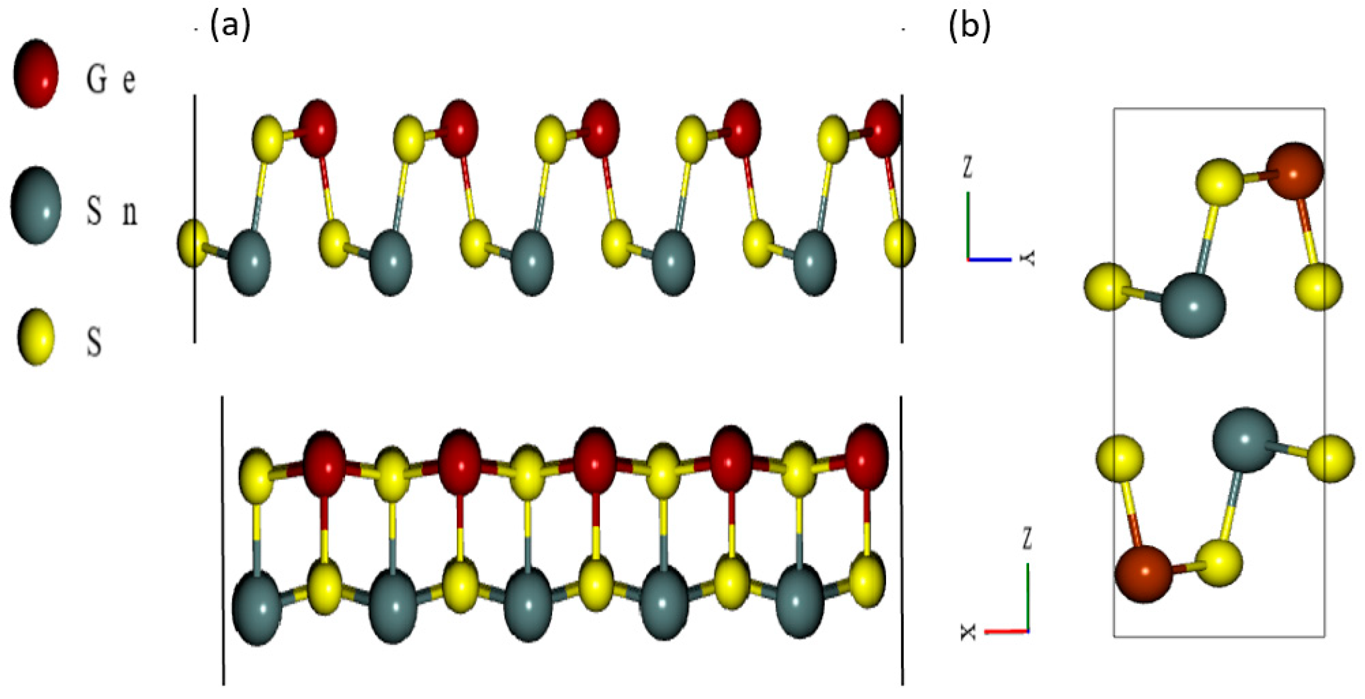
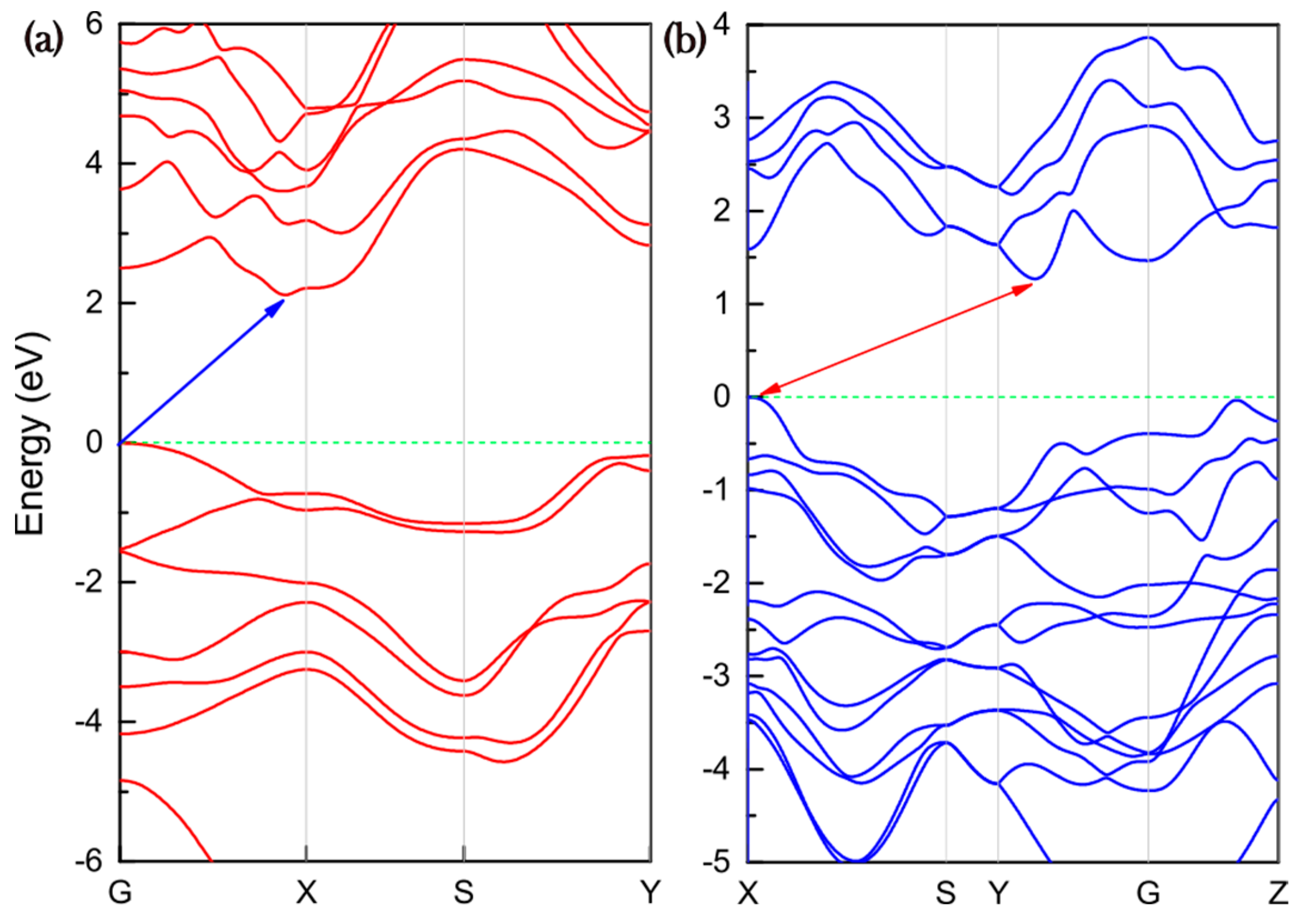
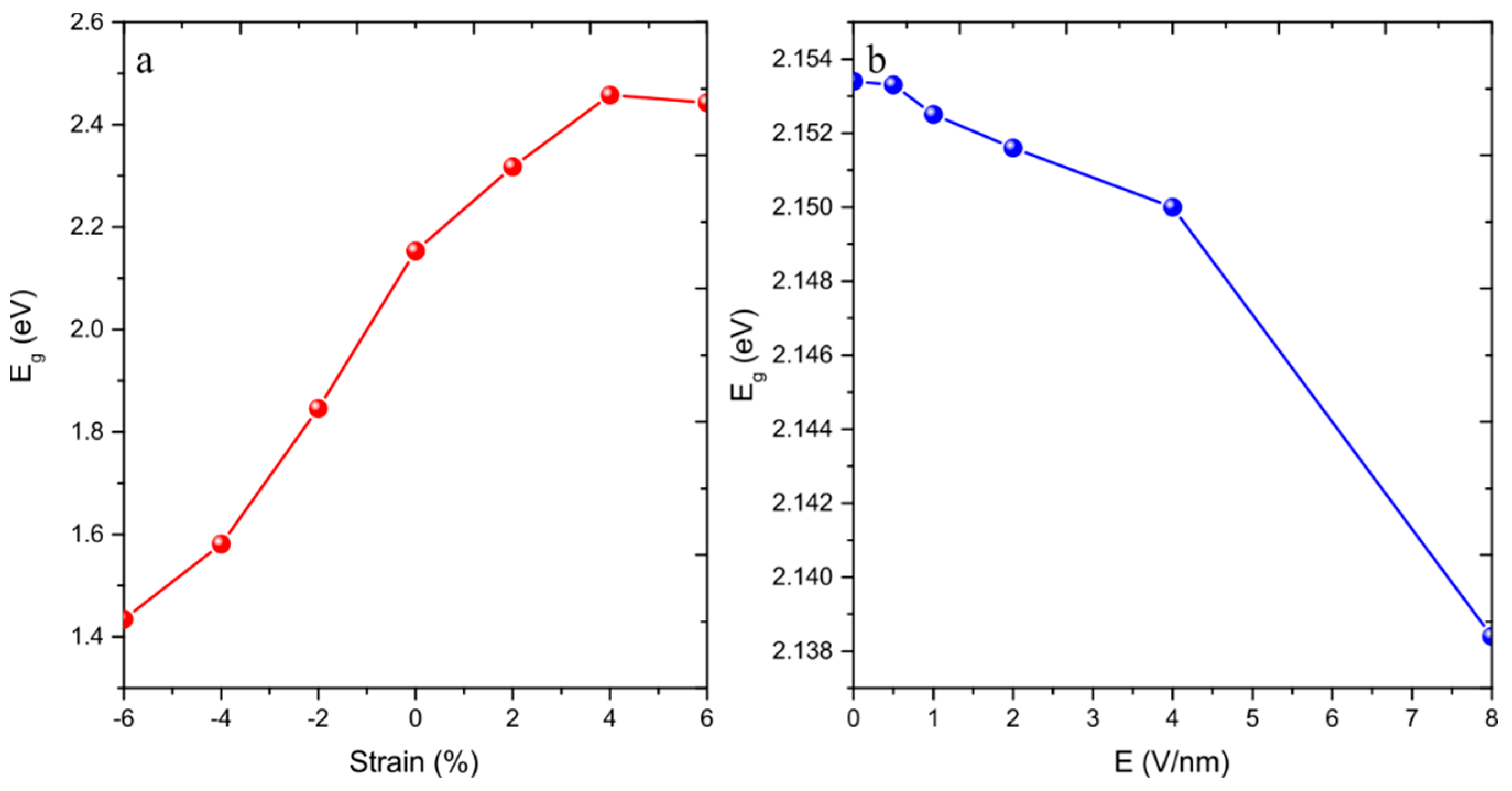
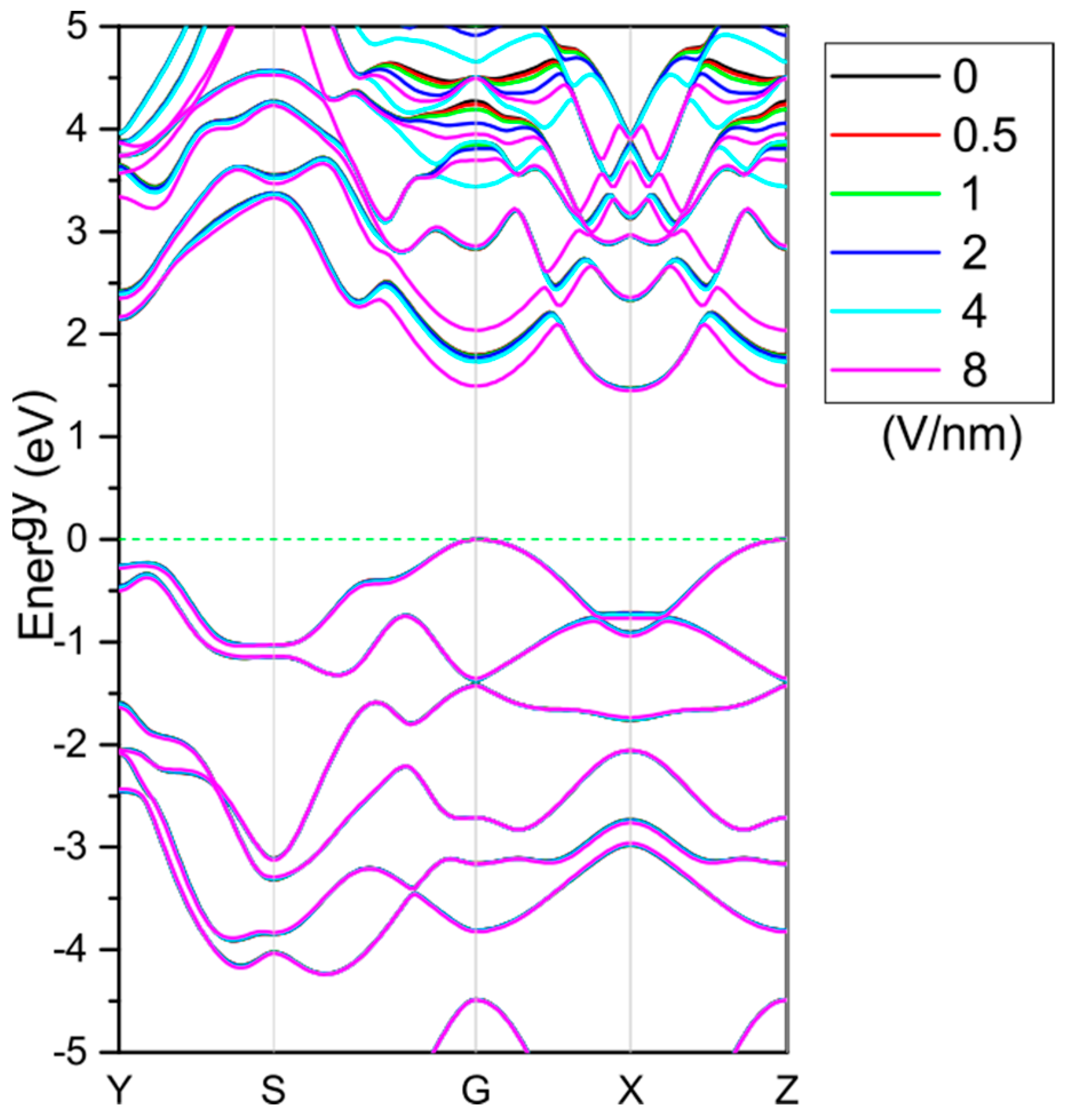
3. Results and Discussion

For our computation, we chose the bulk GeS crystal structure with space group Pnma and lattice parameter values of a = 4.3827 Å, b = 4.2322 Å, and c = 11.6360 Å [18] as the starting structure model. To prevent interlayer interactions, we adjusted the value of c to 28 Å and kept a and b identical to the bulk. Figure 1 shows the top and side views of the GeSnS2 monolayer. The GeSnS2 monolayer is an orthorhombic crystal type with one Sn atom covalently bound to one Ge and two Se atoms. Unlike graphene, which has a planar 2D nanostructure, the GeSnS2 structure has a puckered honeycomb structure. The directional orientation of the monolayer affects its characteristics. After the relaxation, we present in Table 1 the obtained lattice parameters of the bulk and monolayer GeSnS2 compared with the bulk and monolayer SnS and GeS.
In this study, we first compute the band structures of the GeSnS2 monolayer in its equilibrium state, as shown in Figure 2, focusing on its electrical characteristics. The results reveal that the GeSnS2 monolayer is a semiconductor at equilibrium, exhibiting a significant indirect bandgap of 2.15 eV. This finding is consistent with the outcomes of previous DFT simulations [13,14,15,16]. Additionally, we found that the bandgap of the GeSnS2 bulk is 1.37 eV lower than its monolayer counterpart. For the bulk, the conductor band minimum (CBM) is located near the Y-point, and the valence band maximum (VBM) is located at the X-point, resulting in an indirect bandgap. In contrast, for the GeSnS2 monolayer, the VBM is located at the gamma-point and the CBM is near the X-point. The observed difference in the band structure between the bulk and monolayer of GeSnS2 is attributed to the confinement effect, which also opened the band gap from 1.37 to 2.15 eV. Interestingly, the bandgap of our material is strongly influenced by the material’s thickness, as reported for other 2D materials like BP [9]. Given the slight energy difference between the electronic states at the top and bottom of the valence and conduction bands, located at the X and gamma-points, we anticipate that the band structures of the GeSnS2 monolayer can be significantly altered by the effects of either strain (b) or an external electric field (E).
The study of changes in electrical characteristics caused by external influences, such as deformation or external fields, is crucial in designing devices such as nanoelectromechanical devices or sensors. Capturing the changing laws of material characteristics resulting from these events provides us with several alternatives for applying them to specific devices.
To explore the impact of strain engineering on the electrical characteristics of the GeSnS2 monolayer, a biaxial strain ranging from −6% to 6% is applied to its two-dimensional surface. The “+” and “−” marks represent the tensile and compressive examples of the biaxial strain, respectively. This range of strain allows us to investigate the effects of different levels of strain on the monolayer’s electrical properties, which can inform the design of devices that rely on these characteristics.
Figure 3 presents the strain-dependent band gap of the Janus GeSnS2 monolayer. The band gaps show a continuous decrease under a biaxial compressive strain, while a biaxial stretched strain has the opposite effect. Specifically, as shown in Figure 3a, the bandgap changes from 2.15 eV to 1.43 eV as the strain changes from 0% to −6%. On the other hand, tensile strain has changed the band gap from 2.15 to 2.44 eV.
Interestingly, the semiconductor-metal phase transition can be induced by very high compression. GeSnS2 monolayers offer excellent opportunities for use in nanoelectromechanical devices because their electrical properties can be readily modified by strain engineering. This makes them a promising candidate for developing novel electronic and optoelectronic devices with advanced functionalities.
In this section, we investigate how the electronic properties of the GeSnS2 monolayer are affected by a perpendicular electric field labeled “E”. This electric field is applied perpendicular to the GeSnS2 monolayer’s 2D plane to analyze the monolayer’s electronic characteristics under the influence of electricity. We apply the electric field in the z-positive axis direction and vary it from 0 V/nm to 8 V/nm (0.5, 1, 2, 4, and 8 V/nm). We present the effects of the external field E on the GeSnS2 monolayer’s band gap energy in Figure 3. Our findings indicate that the band gap energy of the GeSnS2 monolayer changes slightly with a positive electric field. Our computed results reveal that the band gap energy of the GeSnS2 monolayer is 2.153 eV and 2.138 eV at E = 0 V/nm and E = 8 V/nm, respectively.
In order to get a better insight into the effect of the electric field, we present the band structures of the GeSnS2 monolayer in Figure 4. As we can see in this figure, the conduction band is more sensitive to the electric field than the valance band. We also observe that the diminution of the band gap is attributed to the shift in the conduction band. A transition from an indirect to a direct band gap occurs when an electric field of 8 V/nm is applied, even though there is no major change in the band gap energy. The band gap is transformed from Gamma-X to a direct band gap at Gamma with an energy of 2.138 eV.
The ability to manipulate electronic properties, particularly through the application of an external field, makes it even more attractive for use in these applications. One important characteristic that can be controlled is the transition from an indirect to a direct semiconductor, which significantly impacts the efficiency of electron transport and, ultimately, the device’s performance. By exploiting this characteristic, GeSnS2 can potentially be used in various applications, such as developing highly efficient and compact nanoelectronic devices. The ability to precisely manipulate the electronic properties of GeSnS2 monolayers at the nanoscale level opens up new opportunities for advancing nanoelectronics and designing novel devices with unprecedented performance.

4. Conclusions

In our research, we investigated the modulation of the electronic band structures of the GeSnS2 monolayer through external electric fields and strain. Our findings reveal that external electric fields can effectively tune the band gap of the GeSnS2 monolayer, providing a promising avenue for designing high-performance electronic devices. Additionally, we demonstrated that both tensile and compressive strain could alter the electronic band structures of the GeSnS2 monolayer, allowing for further control over its electronic properties. Furthermore, we observed that electric fields could slightly change the band gap of semiconductors, with the possibility of an indirect-direct bandgap transition occurring at specific electric field intensities. By carefully controlling these factors, we can unlock the full potential of semiconductors and pave the way for a wide range of innovative and high-performance electronic devices.

Author Contributions

Conceptualization, E.M.F. and L.M.P.; methodology, J.E.h.; software, J.E.h., L.M.P.; validation, E.M.F.; formal analysis, L.M.P.; investigation, J.E.h.; resources, L.M.P., E.M.F.; data curation, J.E.h.; writing—original draft preparation, J.E.h.; writing—review and editing, J.E.h.; visualization, J.E.h.; supervision, E.M.F., L.M.P.; project administration, E.M.F., L.M.P.; funding acquisition, L.M.P. All authors have read and agreed to the published version of the manuscript.

Funding

L.M.P. acknowledges financial support from ANID through Convocatoria Nacional Subvención a Instalación en la Academia Convocatoria Año 2021, Grant SA77210040.

Institutional Review Board Statement

Not applicable.

Informed Consent Statement

Not applicable.

Data Availability Statement

No data was used in this paper.

Conflicts of Interest

The authors declare no conflict of interest.

References

  1. Novoselov, K.S.; Geim, A.K.; Morozov, S.V.; Jiang, D.; Zhang, Y.; Dubonos, S.V.; Grigorieva, I.V.; Firsov, A.A. Electric field effect in atomically thin carbon films. Science 2004, 306, 666–669. [Google Scholar] [CrossRef]
  2. Lin, Y.-M.; Jenkins, K.A.; Valdes-Garcia, A.; Small, J.P.; Farmer, D.B.; Avouris, P. Operation of Graphene Transistors at Gigahertz Frequencies. Nano Lett. 2009, 9, 422–426. [Google Scholar] [CrossRef] [PubMed]
  3. Mas-Ballesté, R.; Gómez-Navarro, C.; Gómez-Herrero, J.; Zamora, F. 2D materials: To graphene and beyond. Nanoscale 2010, 3, 20–30. [Google Scholar] [CrossRef] [PubMed]
  4. Randviir, E.P.; Brownson, D.A.C.; Banks, C.E. A decade of graphene research: Production, applications and outlook. Mater. Today 2014, 17, 426–432. [Google Scholar] [CrossRef]
  5. Coleman, J.N.; Lotya, M.; O’Neill, A.; Bergin, S.D.; King, P.J.; Khan, U.; Young, K.; Gaucher, A.; De, S.; Smith, R.J.; et al. Two-Dimensional Nanosheets Produced by Liquid Exfoliation of Layered Materials. Science 2011, 331, 568–571. [Google Scholar] [CrossRef]
  6. Yarmohammadi, M. Electronic miniband structure, heat capacity and magnetic susceptibility of monolayer and bilayer silicene in TI, VSPM and BI regimes. Phys. Lett. A 2017, 381, 1261–1267. [Google Scholar] [CrossRef]
  7. Hoi, B.D.; Yarmohammadi, M. The Kubo-Greenwood spin-dependent electrical conductivity of 2D transition-metal dichalcogenides and group-IV materials: A Green’s function study. J. Magn. Magn. Mater. 2018, 451, 57–64. [Google Scholar] [CrossRef]
  8. Ren, X.; Lian, P.; Xie, D.; Yang, Y.; Mei, Y.; Huang, X.; Wang, Z.; Yin, X. Properties, preparation and application of black phosphorus/phosphorene for energy storage: A review. J. Mater. Sci. 2017, 52, 10364–10386. [Google Scholar] [CrossRef]
  9. Carvalho, A.; Wang, M.; Zhu, X.; Rodin, A.S.; Su, H.; Neto, A.H.C. Phosphorene: From theory to applications. Nat. Rev. Mater. 2016, 1, 16061. [Google Scholar] [CrossRef]
  10. Seixas, L. Janus two-dimensional materials based on group IV monochalcogenides. J. Appl. Phys. 2020, 128, 045115. [Google Scholar] [CrossRef]
  11. Sivasamy, R.; Amirthaganesan, S.; Espinoza-González, R.; Quero, F.; Batoo, K.M. First-principles investigation of the electronic structure, optical and thermodynamic properties on monolayer Sn0.5Ge0.5Se nanosheet. Phys. E Low-Dimens. Syst. Nanostructures 2021, 126, 114454. [Google Scholar] [CrossRef]
  12. Pham, K.D. Theoretical prediction of structural, mechanical, and electronic properties of Janus GeSnX2 (X = S, Se, Te) single-layers. RSC Adv. 2021, 11, 36682–36688. [Google Scholar] [CrossRef] [PubMed]
  13. Giannozzi, P.; Baroni, S.; Bonini, N.; Calandra, M.; Car, R.; Cavazzoni, C.; Ceresoli, D.; Chiarotti, G.L.; Cococcioni, M.; Dabo, I.; et al. QUANTUM ESPRESSO: A modular and open-source software project for quantum simulations of materials. J. Phys. Condens. Matter 2009, 21, 395502. [Google Scholar] [CrossRef] [PubMed]
  14. Heyd, J.; Scuseria, G.E.; Ernzerhof, M. Hybrid functionals based on a screened Coulomb potential. J. Chem. Phys. 2003, 118, 8207–8215. [Google Scholar] [CrossRef]
  15. El hamdaoui, J.; Lakaal, K.; Mazkad, D.; Beraich, M.; El Fatimy, A.; Courel, M.; Pérez, L.M.; Díaz, P.; Laroze, D.; Feddi, E. First principles study on electronic and optical properties of Cu2CoGeS4 for photovoltaic conversion and photocatalytic applications. Mater. Res. Bull. 2023, 164, 112235. [Google Scholar] [CrossRef]
  16. El Hamdaoui, J.; El-Yadri, M.; Farkous, M.; Kria, M.; Courel, M.; Ojeda, M.; Pérez, L.M.; Tiutiunnyk, A.; Laroze, D.; Feddi, E.M. Strain Effects on the Electronic and Optical Properties of Kesterite Cu2ZnGeX4 (X = S, Se): First-Principles Study. Nanomaterials 2021, 11, 2692. [Google Scholar] [CrossRef] [PubMed]
  17. El Hamdaoui, J.; Kria, M.; Lakaal, K.; El-Yadri, M.; Feddi, E.M.; Pedraja Rejas, L.; Pérez, L.M.; Díaz, P.; Mora-Ramos, M.E.; Laroze, D. Ab Initio Study of Carrier Mobility, Thermodynamic and Thermoelectric Properties of Kesterite Cu2ZnGeS4. Int. J. Mol. Sci. 2022, 23, 12785. [Google Scholar] [CrossRef] [PubMed]
  18. Fei, R.; Li, W.; Li, J.; Yang, L. Giant piezoelectricity of monolayer group IV monochalcogenides: SnSe, SnS, GeSe, and GeS. Appl. Phys. Lett. 2015, 26, 173104. [Google Scholar] [CrossRef]
Figure 1. (a) Top and side monolayer views; (b) the bulk structure of GeSnS2.
Materproc 14 00059 g001
Figure 2. The band structure of (a) the monolayer and (b) the bulk of GeSnS2.
Materproc 14 00059 g002
Figure 3. The variation of band gap energy with (a) strain (red curve) and (b) an electric field (blue curve).
Materproc 14 00059 g003
Figure 4. The effect of an electric field on the band structure of monolayer GeSnS2.
Materproc 14 00059 g004
Table 1. The computed lattice parameters and band gap energy of GeSnS2 bulk and monolayer.
a (Å)b (Å) c (Å)Eg (eV)
Monolayer GeSnS24.523.82 2.15 (hse)
Bulk GeSnS24.433.8411.081.37 (hse)
Disclaimer/Publisher’s Note: The statements, opinions and data contained in all publications are solely those of the individual author(s) and contributor(s) and not of MDPI and/or the editor(s). MDPI and/or the editor(s) disclaim responsibility for any injury to people or property resulting from any ideas, methods, instructions or products referred to in the content.

