Proceeding Paper

Current Density-Voltage (J-V) Characterization of Monolithic Nanolaminate Capacitors †

by
Zeinab Mousavi Karimi
* and
Jeffrey A. Davis
School of Electrical and Computer Engineering, Georgia Institute of Technology, Atlanta, GA 30332, USA
*
Author to whom correspondence should be addressed.
Presented at the 4th International Online Conference on Nanomaterials, 5–19 May 2023; Available online: https://iocn2023.sciforum.net.
Mater. Proc. 2023, 14(1), 54; https://doi.org/10.3390/IOCN2023-14590
Published: 12 June 2023
(This article belongs to the Proceedings of The 4th International Online Conference on Nanomaterials)

Abstract

:
In a world of miniaturized electronics, there is a rapidly increasing need for reliable, efficient, and compact energy storage systems with low-loss dielectrics. To address this need, this work proposes the development of compact, micro-capacitive energy storage devices compatible with IC processing so that they can be integrated monolithically on-chip. There are two main approaches to the fabrication of integrated on-chip micro-supercapacitor energy storage devices: interdigitated electrode (IDE) devices and parallel plate electrode (PPE) devices. As part of the design of such systems, this study aims to investigate the behavior of current density-voltage (J-V) in homogeneous and heterogeneous IDE and PPE devices to determine whether the anomalies between the interfaces of dielectric materials in such structures affect their leakage current. The ultimate goal is to design a solid-state capacitor energy storage module with low-loss dielectrics, high energy densities, and improved areal capacitance density that can offer a high number of charge/discharge cycles for portable power electronics. An understanding of J-V characteristics is crucial in achieving this objective. Specifically, this paper will explore and investigate nanolaminate, solid-state PPE, and IDE capacitive energy storage “modules” fabricated using nanolithographic techniques. The dielectric layers in these structures are composed of alternating nanolaminate layers of thin higher-k Al 2 O 3 and lower-k SiO 2 . Recent findings have shown that capacitive energy storage devices made from a large number of these on-chip multilayer nanolaminate energy storage PPE (MNES-PPE) structures that utilize the interfacial anomalies of thin high-k/SiO 2 nanolaminates could have the potential to overcome many of the limitations of current compact energy storage technologies. Preliminary projections indicate that these high-density nanolaminate capacitors with laminate thicknesses around 5 nm could produce devices with high volumetric energy densities ( 290 J/cm 3 ) that are significantly higher than conventional supercapacitors ( 20 J/cm 3 ).

1. Introduction

Currently available electrochemical batteries have the disadvantage of low power density, which restricts their use in applications that require high pulse power. Supercapacitors, on the other hand, have electrodes and electrolytes that can deteriorate after heavy use [1], despite having energy density about an order of magnitude smaller than lead-acid batteries [2]. These devices also suffer from low breakdown voltages, limiting their energy density [1]. Despite research efforts in advanced solid-state dielectrics, such as ferroelectric polymers [3], superlattices [4], and doped ferroelectrics [5], which aim to match the energy density of supercapacitors, they are not currently viable alternatives due to their lack of high breakdown field strengths [6].
Multiple factors affect the breakdown field strength and leakage current in devices, such as bonding structure, interfacial properties, materials’ bandgap, the mean-free path of electrons, and possible electron tunneling mechanisms. In high-k materials, where narrow bandgaps can result in significant loss, inserting a higher bandgap insulator between electrodes and nanolaminate layers can substantially reduce leakage current and enhance breakdown strength [7,8,9]. For example, researchers in [7] found that a 5 nm Al 2 O 3 interfacial layer optimizes the dielectric properties of Al 2 O 3 /TiO x nanolaminates, reducing leakage current density while maintaining high dielectric constant. However, refs. [7,9] demonstrated that using an ultra-thin interfacial Al 2 O 3 layer (less than 2 nm) can cause direct tunneling, leading to a decrease in breakdown field strength.
One of the possible ways to develop solid-state capacitive energy storage devices with high permittivity, significant energy and power density, low leakage, and an enormous number of recharge cycles is to incorporate certain low loss, high-breakdown field strength materials such as Al 2 O 3 , HfO 2 , ZrO 2 , Si 3 N 4 , and SiO 2 into existing nanotechnologies [10] as multilayer nanolaminates. The interfacial permittivity of these dielectric nanolaminates and its impact on the current density-voltage (J-V) relationship are typically two of the most important electrical parameters to be understood and characterized.
The primary goal of this study is to enhance our comprehension of the current density-voltage (J-V) behavior in homogeneous and heterogeneous parallel plate electrode (PPE) and interdigitated electrode (IDE) devices by using experimental findings and 2-D finite element method (FEM) simulation models. The study aims to determine whether anomalies at the dielectric/dielectric material interface in such structures negatively impact the leakage current in a monolithic capacitor energy storage system. The insights gained from this investigation will be utilized to suggest the design of a high-density energy storage device with minimal loss and high breakdown voltage in Section 4 of this research.

2. Materials and Methods

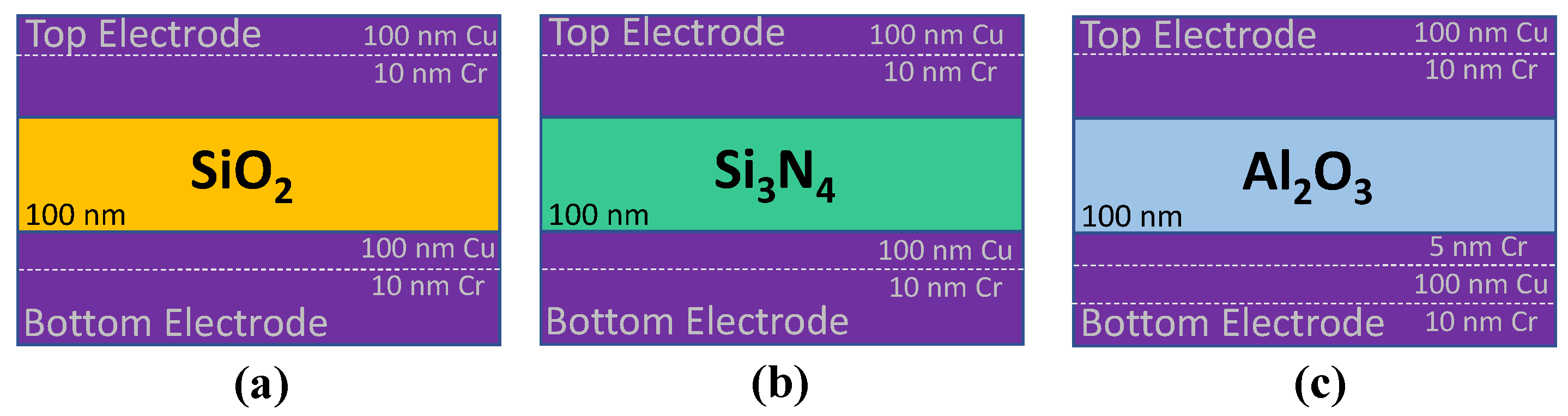
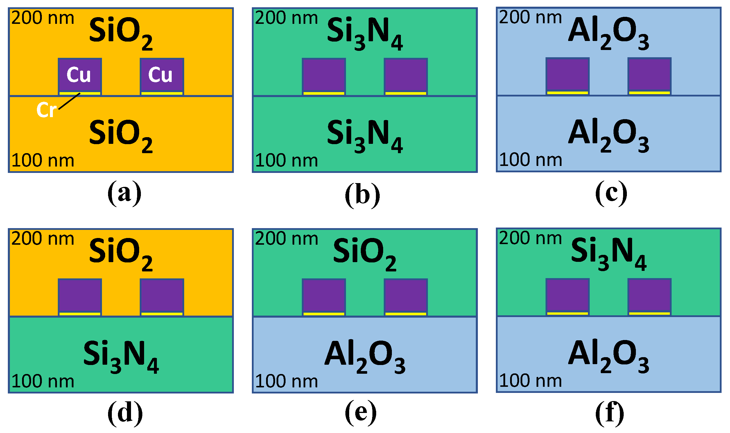
2.1. Overview of Fabrication of PPE and IDE Devices

In this work, initially, the PPE devices with plate areas of 76 μm by 76 μm are fabricated on p-type silicon substrates with < 100 > orientation and resistivity of 8–12 Ω ·cm. The top and bottom metal electrodes are evaporated using a Denton Explorer e-beam evaporator tool. Next, 100 nm SiO 2 and Si 3 N 4 dielectric layers are deposited using a Unaxis plasma enhanced chemical vapor deposition (PECVD) system on the first two PPE devices, and 100 nm of Al 2 O 3 is e-beam evaporated for the third device as shown in Figure 1. The capacitance and conductance values of the PPEs are measured using HP4284A LCR four-point probe meter at f = 1 kHz with an AC amplitude of 1 V with zero offset bias. The measured capacitance values are used to extract the relative permittivities of SiO 2 , Si 3 N 4 , and Al 2 O 3 as k SiO 2 = 4.3, k Si 3 N 4 = 6.6 and k Al 2 O 3 = 9.9, respectively, by means of an analytical parallel plate model and the corresponding simulation models.
Using Si wafers with the aforementioned characteristics, three homogeneous and three heterogeneous IDE devices are fabricated with different combinations of SiO 2 , Si 3 N 4 , and Al 2 O 3 as shown in Figure 2. Initially, 900 nm of SiO 2 is deposited to provide an isolation layer. The wafer with the 900 nm SiO 2 layer is then cleaved using a diamond scribe into six samples. Next, the SiO 2 and Si 3 N 4 layers are deposited on the samples using PECVD, and the Al 2 O 3 is e-beam evaporated. The thickness of the first 900 nm SiO 2 layer is verified using a Nanospec Reflectometer, and for the 100 nm SiO 2 , Si 3 N 4 and Al 2 O 3 layers, a Woollam M2000 Ellipsometer is used. All samples are then spin-coated using an A6 950-polymethylmethacrylate (PMMA) solution and are exposed using an Elionix ELS-G100 electron beam lithography (EBL) system at an exposure current of 3 nA. IDE capacitors with 1000 interleaved electrodes that have spacings of 200 nm are fabricated on each of the six samples using the EBL. The resulting patterns are developed in a mixture of one part methyl isobutyl ketone (MIBK) and one part isopropanol (IPA) and are inspected post-development using an Olympus MX61 Microscope. Next, the IDE electrodes and contact pads required for electrical measurements are formed by evaporating 10 nm of Cr and 100 nm of Cu using the e-beam tool. The PMMA residues on the samples are then lifted off by immersing the samples in a Microposit Remover 1165 and heating the solvent at 120 C for 2 h. After the lift-off, the samples are triple-cleaned using IPA, acetone, and methanol and inspected using an Olympus MX61 Microscope. The widths of the IDE electrodes and the spacings between them are verified using a Hitachi S-4700 scanning electron microscope (SEM).
Similar to the PPE devices, the capacitance and conductance values of the six IDE devices are measured using the HP4284A LCR 4-point probe meter under ambient conditions at f = 1 kHz with an AC amplitude of 1 V with zero offset bias at standard room temperature (25 C). These measurements are explained in more detail in [11]. The devices are then encapsulated with 200 nm SiO 2 , Si 3 N 4 , and Al 2 O 3 layers as shown in Figure 2. As the last step of fabrication, the electrical contact pads of the devices are exposed using the EBL, developed, and thoroughly inspected.

2.2. Current-Voltage (I-V) Measurements

The I-V measurements on PPE and IDE devices are conducted using a Keithley 2450 Source Meter (SMU) instrument. These measurements aim to perform I-V testing that allows for the measurement of low current densities before dielectric breakdown occurs. The measurements are taken at low applied voltages to avoid damaging the PPE or IDE devices. A standard room temperature of 25 C is maintained during the I-V measurements for both devices. Seven devices from each PPE and IDE structure are tested, resulting in 84 I-V measurements. The results of these electrical measurements are averaged and presented in Section 3 of this paper.

3. Results

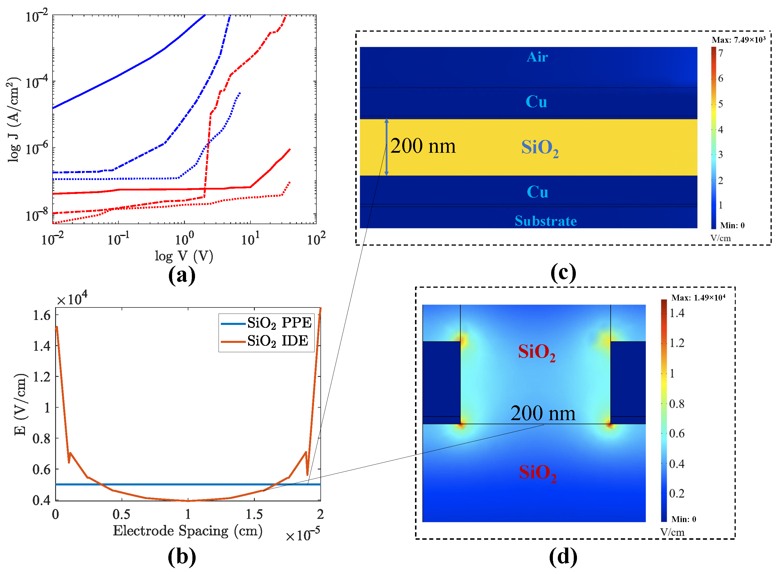
3.1. Homogeneous PPE and IDE Devices

Figure 3a illustrates the current density-voltage (J-V) plot that compares the homogeneous IDE and PPE structures. It is evident from the plot that the IDE geometry exhibits a higher leakage current than the PPE geometry. For instance, the SiO 2 device with homogeneous IDE has a leakage current that is orders of magnitude larger than that of the SiO 2 PPE device. Similarly, there is an approximate order of magnitude difference in leakage currents between the Si 3 N 4 IDE and Si 3 N 4 PPE and between the Al 2 O 3 IDE and Al 2 O 3 PPE structure, as depicted in Figure 3a. Notably, these differences in leakage are observed in homogeneous IDE and PPE devices that lack anomalous interfacial planes, which could cause additional low resistance current paths.
At V = 0.1 V, Figure 3b displays the electric field profile of both homogeneous IDE and PPE structures. In the homogeneous IDE SiO 2 device, the electric field varies between the adjacent electrode finger, with the highest fields situated at the edges of the electrodes (Figure 3c). Conversely, in the PPE SiO 2 structure, the electric field remains consistent between two parallel electrodes, as demonstrated in Figure 3d. The non-uniformity of electric fields in IDEs compared to PPEs can be attributed to the differences in the geometries of the electrodes. The fingers in the IDEs create a series of capacitors, which results in a non-uniform and complex distribution of electric fields along the electrodes [12,13]. The high fields around the IDE electrode could be a source of high carrier injection into the dielectric, while the PPE structure lacks these high fields entirely. Non-trivial carrier injection can occur when the electric field strength around the IDE electrodes exceeds a certain threshold, and the energy barrier of the dielectric material can be overcome, leading to the generation of charge carriers. After injection, these high fields could also initiate impact ionization, increasing the dielectric conductivity and leakage in the capacitor device. The aforementioned observations imply that a PPE electrode design would be more effective in significantly reducing leakage currents for a forthcoming energy storage device. However, due to their sensitivity to this electrical characteristic, IDE structures remain better suited for exploring tangential interfacial permittivity.

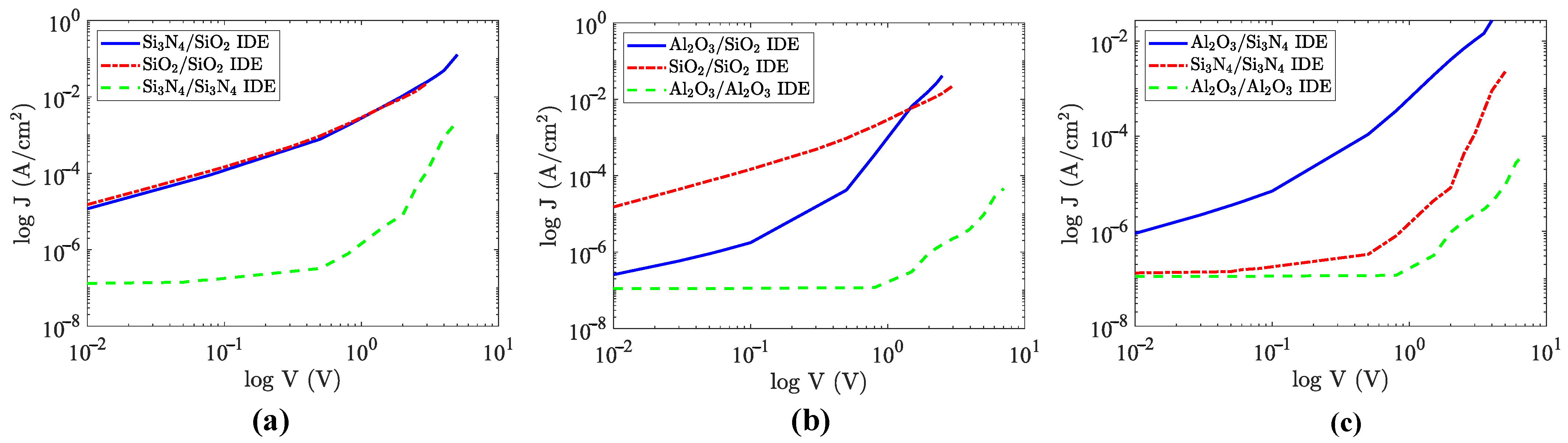
3.2. Homogeneous vs. Heterogeneous Structure in IDE Devices

Figure 4 illustrates the current densities of both homogeneous and heterogeneous encapsulated IDE devices. In Figure 4a, the J-V characteristics of Si 3 N 4 /SiO 2 and SiO 2 IDE structures are quite similar. This suggests that leakage is primarily dominated by the bulk oxide between the electrodes, and consequently, the Si 3 N 4 /SiO2 interface has minimal impact on device leakage. This experimental result holds significance since prior research in [14] identified the interfacial permittivity to be very high (k Si 3 N 4 / SiO 2 1419 ). Therefore, this finding strongly suggests that the Si 3 N 4 /SiO 2 material combination may be a feasible candidate for future device designs.
Furthermore, the J-V characteristic plots of the Al 2 O 3 /SiO 2 , SiO 2 , and Al 2 O 3 IDE structures indicate that the inclusion of the interface has minimal impact on the overall leakage current. In Figure 4b, the Al 2 O 3 /SiO 2 device exhibits an order of magnitude lower leakage current than the homogeneous SiO 2 IDE device, but higher leakage compared to the homogeneous Al 2 O 3 IDE structure. This suggests that the heterogeneous Al 2 O 3 /SiO 2 structure features a relatively low-leakage interface. Such low leakage, coupled with the high interfacial permittivity (k Al 2 O 3 / SiO 2 2373 [14]), provides strong encouragement for incorporating this Al 2 O 3 /SiO 2 interface into future energy storage devices. However, there is an interface that appears to exacerbate leakage current. Figure 4c demonstrates that the higher leakage current in the Al 2 O 3 /Si 3 N 4 heterogeneous IDE structure compared to the other two homogeneous IDE devices indicates that the addition of the heterogeneous interface has degraded the quality of the Al 2 O 3 /Si 3 N 4 heterogeneous device. This could be attributed to more complex interfacial trap states in this structure. Consequently, this outcome suggests that incorporating this interface into an energy storage device would not be suitable.

4. Discussion

Potential Application of Ideal High-Density PPE Devices

This section examines the potential of the previously fabricated homogeneous and heterogeneous IDE and PPE devices to be used as potential candidates for energy storage devices. A new device architecture that utilizes on-chip PPE structures and the directional interfacial anomalies of very thin (5 nm) SiO 2 and Al 2 O 3 nanolaminates is proposed as a possible solution to overcome the shortcomings of current energy storage technologies.
The PPE and IDE structures, both homogeneous and heterogeneous, depicted in Figure 1 and Figure 2 have been evaluated for their breakdown voltage. The J-V characteristics of these structures in Section 3 and the estimated breakdown voltage values for all the fabricated PPE and IDE structures were considered to identify the optimal energy storage device. The recommended device comprises thin nanolaminate dielectric layers of Al 2 O 3 /SiO 2 that are deposited so that the interface layers are perpendicular to the metallic electrodes, enabling the highly polarizable interfaces of these layers to be activated more efficiently, as illustrated in Figure 5.
The PPE structure of a theoretical multilayer nanolaminate energy storage system (MNES) is presented in Figure 5. This model, which was simulated using COMSOL Multiphysics® (COMSOL, Inc., Stockholm, Sweden), consists of 18 alternating layers of 5 nm SiO 2 (k SiO 2 = 4.3) and Al 2 O 3 (k Al 2 O 3 = 9.9), with a 1 nm high-k interfacial layer (k Al 2 O 3 / SiO 2 = 2373), placed between capacitor electrodes with a spacing of 200 nm. The value of the interfacial high-k and the model itself have been extracted from experimental data described in [14,15]. The maximum storage voltage V m a x for the MNES PPE configuration shown in Figure 5 can be calculated using:
V m a x = β V b d = β E b d d ,
where β is the maximum charging factor, V b d is the breakdown voltage, E b d is the breakdown field strength of the dielectric material, and d is the distance between the electrodes. SiO 2 has a breakdown field strength of ∼15 MV/cm, and Al 2 O 3 has a breakdown field strength of ∼10 MV/cm, according to [16] and [17], respectively. Thus, assuming a maximum breakdown factor of β = 0.5, the breakdown voltages of SiO 2 and Al 2 O 3 are calculated to be ∼300 V and ∼200 V, respectively. Assuming that the breakdown of these materials is roughly half the strength of the weakest dielectric material in the laminate structure, i.e., β = 0.5, the structure depicted in Figure 5 is then simulated at a maximum voltage of V b d = 100 V. The resulting simulated capacitance C, which accounts for overhead capacitances, is calculated to be 0.1 pF. The maximum volumetric energy density for the multilayer nanolaminate U v o l can be calculated using:
U v o l = E n e r g y V o l u m e = C V m a x 2 2 · 1 d e v i c e v o l u m e
The MNES PPE energy storage device depicted in Figure 5 with 5 nm Al 2 O 3 /SiO 2 multilayers, assuming β = 0.5, has a maximum obtainable volumetric energy density U v o l of approximately 293 J/cm 3 when operated at a maximum voltage of V m a x = 100 V. The corresponding current density is estimated to be around ∼10 nA/cm 2 . Notably, this volumetric energy storage value is 36× greater than that of an energy storage device of the same dimension with only Al 2 O 3 deposited between the electrodes.

5. Conclusions

In this work, the current density-voltage characteristics of homogeneous and heterogenous IDE and PPE structures with SiO 2 , Si 3 N 4 , and Al 2 O 3 nanolaminates are investigated using experimental data and FEM simulations. The high breakdown field strengths of the materials examined in this work suggest that there may be potential for energy storage in capacitive devices that leverage the experimental findings and simulation results. In particular, preliminary J-V measurements and simulation projections showed that PPE capacitive devices with a high density of Al 2 O 3 /SiO 2 nanolaminates with a laminate thickness of approximately 5 nm could produce devices with volumetric energy densities that are around 15× greater (i.e., ∼290 J/cm 3 ) compared to conventional electrochemical double layer supercapacitors (i.e., ∼20 J/cm 3 ).

Author Contributions

Z.M.K. and J.A.D. carried out the conceptualization, methodology, software, validation, formal analysis, investigation, and resources. Z.M.K. curated the data, prepared the original draft and did the writing. Z.M.K. and J.A.D. carried out the review and editing. J.A.D. supervised. Z.M.K. and J.A.D. administered the project. J.A.D. took care of the funding acquisition. All authors have read and agreed to the published version of the manuscript.

Funding

This research received no external funding.

Institutional Review Board Statement

Not applicable.

Informed Consent Statement

Not applicable.

Data Availability Statement

Not applicable.

Acknowledgments

This work was performed in part at the Georgia Tech Institute for Electronics and Nanotechnology, a member of the National Nanotechnology Coordinated Infrastructure (NNCI), which is supported by the National Science Foundation (ECCS-1542174).

Conflicts of Interest

The authors declare no conflict of interest.

Abbreviations

The following abbreviations are used in this manuscript:
IDEInterdigitated Electrode
PPEParallel Plate Electrode
MNESMultilayer Nanolaminate Energy Storage
FEMFinite Element Method
PECVDPlasma Enhanced Chemical Vapor Deposition
PMMAPolymethylmethacrylate
EBLElectron Beam Lithography
MIBKMethyl Isobutyl Ketone
SEMScanning Electron Microscope

References

  1. Signorelli, R.; Ku, D.C.; Kassakian, J.G.; Schindall, J.E. Electrochemical Double-Layer Capacitors Using Carbon Nanotube Electrode Structures. Proc. IEEE 2009, 97, 1837–1847. [Google Scholar] [CrossRef]
  2. Wu, Z.S.; Parvez, K.; Feng, X.; Müllen, K. Graphene-Based In-Plane Micro-Supercapacitors with High Power and Energy Densities. Nat. Commun. 2013, 4, 2487. [Google Scholar] [CrossRef] [PubMed] [Green Version]
  3. Sarkar, A.; Ranjith, R.; Krupanidhi, S.B. Nonlinear Dielectric Behavior in Three-Component Ferroelectric Superlattices. J. Appl. Phys. 2007, 102, 024108. [Google Scholar] [CrossRef]
  4. Singh, M.P.; Prellier, W. Oxide Superlattices for Mltiferroics: Opportunities, Issues, and Challenges. Philos. Mag. Lett. 2007, 87, 211–222. [Google Scholar] [CrossRef]
  5. Ang, C.; Yu, Z. High Capacitance-Temperature Sensitivity and “Giant” Dielectric Constant in SrTiO3. Appl. Phys. Lett. 2007, 90, 202903. [Google Scholar] [CrossRef]
  6. Ducharme, S. An Inside-Out Approach to Storing Electrostatic Energy. ACS Nano 2009, 3, 2447–2450. [Google Scholar] [CrossRef] [PubMed]
  7. Lee, G.; Lai, B.K.; Phatak, C.; Katiyar, R.S.; Auciello, O. Interface-Controlled High Dielectric Constant Al2O3/TiOx Nanolaminates with Low Loss and Low Leakage Current Density for New Generation Nanodevices. J. Appl. Phys. 2013, 114, 027001. [Google Scholar] [CrossRef]
  8. Coss, B.E.; Loh, W.Y.; Carlo Floresca, H.; Kim, M.J.; Majhi, P.; Wallace, R.M.; Kim, J.; Jammy, R. Dielectric Dipole Mitigated Schottky Barrier Height Tuning Using Atomic Layer Deposited Aluminum Oxide for Contact Resistance Reduction. Appl. Phys. Lett. 2011, 99, 102108. [Google Scholar] [CrossRef]
  9. Wu, Y.Q.; Lin, H.C.; Ye, P.D.; Wilk, G.D. Current Transport and Maximum Dielectric Strength of Atomic-Layer-Deposited Ultrathin Al2O3 on GaAs. Appl. Phys. Lett. 2007, 90, 072105. [Google Scholar] [CrossRef] [Green Version]
  10. Li, J.Y.; Zhang, L.; Ducharme, S. Electric Energy Density of Dielectric Nanocomposites. Appl. Phys. Lett. 2007, 90, 132901. [Google Scholar] [CrossRef] [Green Version]
  11. Mousavi Karimi, Z. Characterization and Modelling of Anomalous Properties of SiO2, Si3N4, and Al2O3 Nanolaminates. Ph.D. Thesis, Georgia Institute of Technology, Atlanta, GA, USA, 2021. [Google Scholar]
  12. Santos-Neto, I.S.D.; Carvalho, C.D.; Filho, G.B.A.; Andrade, C.D.S.S.; Santos, G.C.D.O.; Barros, A.K.; Neto, J.V.D.F.; Casas, V.L.P.; Alencar, L.M.R.; Lopes, A.J.O.; et al. Interdigitated Electrode for Electrical Characterization of Commercial Pseudo-Binary Biodiesel–Diesel Blends. Sensors 2021, 21, 7288. [Google Scholar] [CrossRef] [PubMed]
  13. Bowen, C.R.; Bowles, A.; Drake, S.; Johnson, N.; Mahon, S. Fabrication and Finite Element Modelling of Interdigitated Electrodes. Ferroelectrics 1999, 228, 257–269. [Google Scholar] [CrossRef]
  14. Mousavi Karimi, Z.; Davis, J.A. Interfacial Permittivity Characterization of Heterogeneous Dielectric Bi-Layers. IEEE Trans. Electron Devices 2022, 69, 1950–1955. [Google Scholar] [CrossRef]
  15. Mousavi Karimi, Z.; Davis, J.A. Permittivity Characterization of Dielectric Surfaces Using Nanofabricated In-Plane Capacitors. IEEE Trans. Electron Devices 2021, 68, 4033–4038. [Google Scholar] [CrossRef]
  16. McPherson, J.; Kim, J.; Shanware, A.; Mogul, H.; Rodriguez, J. Proposed Universal Relationship between Dielectric Breakdown and Dielectric Constant. In Proceedings of the Digest. International Electron Devices Meeting, San Francisco, CA, USA, 8–11 December 2002; pp. 633–636. [Google Scholar]
  17. Lin, H.C.; Ye, P.D.; Wilk, G.D. Leakage Current and Breakdown Electric-Field Studies on Ultrathin Atomic-Layer-Deposited Al2O3 on GaAs. Appl. Phys. Lett. 2005, 87, 182904. [Google Scholar] [CrossRef]
Figure 1. Parallel plate electrode (PPE) devices with (a) SiO 2 , (b) Si 3 N 4 and (c) Al 2 O 3 dielectrics.
Materproc 14 00054 g001
Figure 2. Interdigitated electrode (IDE) devices with (a) SiO 2 /SiO 2 , (b) Si 3 N 4 /Si 3 N 4 , (c) Al 2 O 3 /Al 2 O 3 , (d) Si 3 N 4 /SiO 2 , (e) Al 2 O 3 /SiO 2 and (f) Al 2 O 3 /Si 3 N 4 dielectrics.
Materproc 14 00054 g002
Figure 3. (a) J-V characteristic plots for the SiO 2 , Si 3 N 4 , and Al 2 O 3 homogeneous IDE and PPE devices. Solid blue line represents IDE SiO 2 /SiO 2 ; blue dashed line represents IDE Si 3 N 4 /Si 3 N 4 ; blue dotted line represents IDE Al 2 O 3 /Al 2 O 3 ; solid red line represents PPE SiO 2 ; red dashed line represents PPE Si 3 N 4 ; red dotted line represents PPE Al 2 O 3 . (b) Plot of electric field vs. electrode spacing characteristics between two electrodes for homogeneous (c) PPE SiO 2 , and (d) IDE SiO 2 devices with 200 nm electrode spacing at 0.1 V.
Materproc 14 00054 g003
Figure 4. J-V characteristic plots for the heterogeneous and homogeneous IDE devices with (a) Si 3 N 4 /SiO 2 , SiO 2 , and Si 3 N 4 , (b) Al 2 O 3 /SiO 2 , SiO 2 , and Al 2 O 3 , and (c) Al 2 O 3 /Si 3 N 4 , Si 3 N 4 dielectrics.
Materproc 14 00054 g004
Figure 5. A zoomed FEM model of an multilayer nanolaminate energy storage (MNES) PPE structure composed of 18 alternating layers of Al 2 O 3 /SiO 2 with 1 nm high-k interface.
Materproc 14 00054 g005
Disclaimer/Publisher’s Note: The statements, opinions and data contained in all publications are solely those of the individual author(s) and contributor(s) and not of MDPI and/or the editor(s). MDPI and/or the editor(s) disclaim responsibility for any injury to people or property resulting from any ideas, methods, instructions or products referred to in the content.

