
Antenna-on-Chip for Millimeter Wave Applications Using CMOS Process Technology


Department of Electronic Engineering, National Taipei University of Technology, Taipei 10608, Taiwan
*
Author to whom correspondence should be addressed.
Telecom 2023, 4(1), 146-164; https://doi.org/10.3390/telecom4010010
Submission received: 16 January 2023
/
Revised: 22 February 2023
/
Accepted: 24 February 2023
/
Published: 28 February 2023
(This article belongs to the Special Issue Integrated Circuit and Antenna Design for Millimeter-Wave and Terahertz Communication)
Abstract
:In this paper, a monopole patch antenna is designed, and the structure of the antenna is analyzed. The manufacturing process adopts TSMC 0.18 μm CMOS process technology. An artificial magnetic conductor (AMC) on the M1 layer is proposed in this paper to increase the radiation gain and reduce the reflection coefficient (S11) magnitude for impedance matching and antenna performance. This method can make up for the radiation efficiency and benefits of the antenna-on-chip that are affected by the high dielectric constant and low resistivity of the silicon substrate of the CMOS process. The antenna designed in this paper obtains a simulated bandwidth of 37.5 GHz to 69.5 GHz using the Electromagnetic Simulation Software, and the fractional bandwidth of the design is 60%. Among them, 62 GHz shows a maximum gain value of −2.64 dBi. Actual measurements have confirmed that the reflection coefficient of the antenna on the chip proposed in this paper is the same as the simulation trend, and a wider bandwidth is obtained from 20.9 GHz to 67 GHz, with a fractional bandwidth of 104.89%. This bandwidth covers millimeter wave 28 GHz, 38 GHz, and 60 GHz application frequencies.
1. Introduction
In the future, communication frequency band, millimeter wave, and sub-terahertz (Sub-THz) technologies can meet the requirements of the fifth-generation (5G) communication system. Therefore, to provide a wider bandwidth and faster transmission speed in the communication frequency band at this stage, the communication frequency band is developing towards the millimeter wave frequency band [1,2,3]. However, in some countries such as China and South Korea that use the 6 GHz frequency band, 5G mobile communication has been listed as a commercial frequency band. Hence, many transmission requirements increase, and the frequency bands below 6 GHz can no longer satisfy the transmission requirements of existing users. The millimeter wave is one of the most efficient solutions in improving the transmission efficiency of fifth-generation mobile communication and meeting users’ needs. Through the characteristics of a millimeter wave, it can achieve a low delay, high-speed transmission, and other characteristics to meet the transmission needs of communication users [4,5]. The millimeter wave frequency band has various applications, such as fifth-generation (5G) communication systems, satellite communications, synthetic aperture radars, wideband high-speed point-to-point communications, automotive radars, and other technologies. However, millimeter wave frequency bands have shorter wavelengths than other application frequency bands, so the assembly components are smaller, making wireless systems more compact [6,7].
With the advancement of chip-integrated circuit manufacturing in recent years, component miniaturization can be easily achieved. Additionally, because of the advancement of radio frequency integrated circuits (RFIC), society is gradually paying attention to the concept of the antenna-on-chip. The wavelength of the millimeter wave frequency band is shorter than that of other frequency bands, which is conducive to small-size assembly. Therefore, millimeter wave antennas can be easily fabricated on wafers [6,8,9]. The method of the antenna-on-chip is suitable for making millimeter wave antennas. The antenna-on-chip can avoid mutual influence in the circuit through circuit design such as integrated circuits (IC) [10]. In a transceiver, the antenna is often used as the first and last element of the transmitter and receiver. However, the antenna and transceiver circuit must match the 50 ohm impedance system impedance. The requirement of 50 ohm impedance matching is overcome in the antenna-on-chip. This is because the RF front-end and antenna can be co-designed in the chip, saving the external design area and components [11,12]. There are many challenges in antenna-on-chips. First of all, the Si substrate of the CMOS process is not suitable for the structural design of the antenna because the typical six-layer metal layer CMOS process is the reason that affects the radiation performance and efficiency of the antenna. Second, the distance between the metal layers in the manufacturing process is only 10 μm, the thickness of the Si substrate is 500 μm, and the low resistivity is 10 Ω cm. The above reasons cause most of the electromagnetic waves of the antenna to propagate to the substrate, which greatly reduces the gain of the antenna-on-chip. The high dielectric constant of the Si substrate ( = 11.9) is also a reason for the reduction in the radiation efficiency of the antenna-on-chip. The electromagnetic waves generated by the antenna will be absorbed by the Si substrate instead of propagating into the air, so the radiation efficiency and gain of the antenna-on-chip cannot be compared with traditional typical antennas [13,14,15,16].
Many problems and challenges are often faced in the design of antenna-on-chips. Due to the high dielectric constant and low resistivity of the Si substrate made of wafer CMOS, the gain and radiation efficiency of the antenna-on-chip decrease, resulting in a more significant transmission loss for the antenna-on-chip [14,15].
Recently, antenna-on-chip design has often been considered in area planning and antenna architectures—for example, patch antennas [8,15,17,18,19], numerous meander-line antennas [9], slot antennas [20,21], Yagi-Uda antennas [22], and zig-zag antennas [23]. Among the types of patch antennas, the literature [8] reports a 28 GHz antenna-on-chip for wearable devices, using TSMC 0.18 μm CMOS process technology. The antenna size is 1160 μm × 790 μm. The beam steering of the antenna-on-chip is controlled by a parallel coupler design, and the fractional bandwidth is 84.7%. In [15], the patch antenna is proposed and applied in a millimeter wave frequency band for a 5G communication compact front-end receiver and adopts 28 nm CMOS process technology. This structure enhances the radiation gain of the antenna through the PCB-grounded metal structure and reaches 9.8 dBi. In [17], a patch antenna is used to propose an antenna-on-chip with dual frequency bands. The operating frequencies are 77 GHz and 140 GHz, respectively. The frequency bands fall into 63 GHz–78 GHz and 101 GHz–157 GHz. The fractional bandwidth is 21.28% and 35.21%, and the antenna radiation gain is −3.24 dBi and −5.795 dBi. The dual-band antenna has more advantages in the application. In [18], monopole patch antennas are designed, as well as specially designed square split ring resonators. By coupling to the feeding antenna, additional resonance is generated to solve the disadvantage of the antenna-on-chip gain drop. The literature experiment adopts 0.13 μm SiGe process technology, the working frequency is 81.5 GHz, and it has a gain of 1.61 dBi and a working bandwidth of 77 GHz–87 GHz. In [19], an antenna-on-chip is proposed, which combines a patch antenna with a substrate-integrated waveguide (SIW) and a dielectric resonator antenna (DRA), uses a 65 nm CMOS process with an operating frequency of 94 GHz, and uses an artificial magnetic conductor (AMC) to increase radiation. In [9], a numerous meander-line antenna is proposed, which is applied to the antenna chip in the millimeter wave frequency band. The dual-band operating frequency is 28 GHz and 60 GHz, and it uses 65 nm CMOS process technology. A gain of −10 dBi and a fractional bandwidth of 5.3% were obtained when measured at 28 GHz. A gain of 0 dBi and a fractional bandwidth of 5.9% were obtained when measured at 60 GHz. This antenna-on-chip has the advantage of dual-band 28 GHz and 60 GHz operation in the millimeter wave frequency band. It is applied in the slot antenna of the antenna-on-chip. In [20], a rectangular ring slot antenna is proposed, using a dielectric resonator antenna (DRA) to make the gain of the antenna-on-chip reach 0 dBi at 40 GHz. In [21], the authors specially designed a back-to-back E-type artificial magnetic conductor (AMC) surface-assisted double-diamond slot structure antenna-on-chip, and it is used in the W-frequency band. It adopts 0.13 μm CMOS process technology, and the working frequency band is 80–90 GHz. It has a maximum radiation gain of −0.58 dBi at 84 GHz. The diamond-shaped slot structure antenna array and parasitic elements proposed in this document can obtain a wider bandwidth. In addition, Yagi-Uda antennas are often used as antennas-on-chip. In [22], a solution to the low-gain disadvantage of the antenna-on-chip is proposed, and the Yagi-Uda antenna architecture is designed. Through the basic driving elements, the reflectors and director of the Yagi-Uda antenna and the outer design of the semicircular arc structure increase the radiation gain of the antenna. This design architecture adopts a 180 nm CMOS technology process, the working frequency is 60 GHz, and the radiation gain is −20 dBi. In [23], the zigzag antenna is designed; the system architecture of the antenna-on-chip is proposed and provides high-speed transmission efficiency.
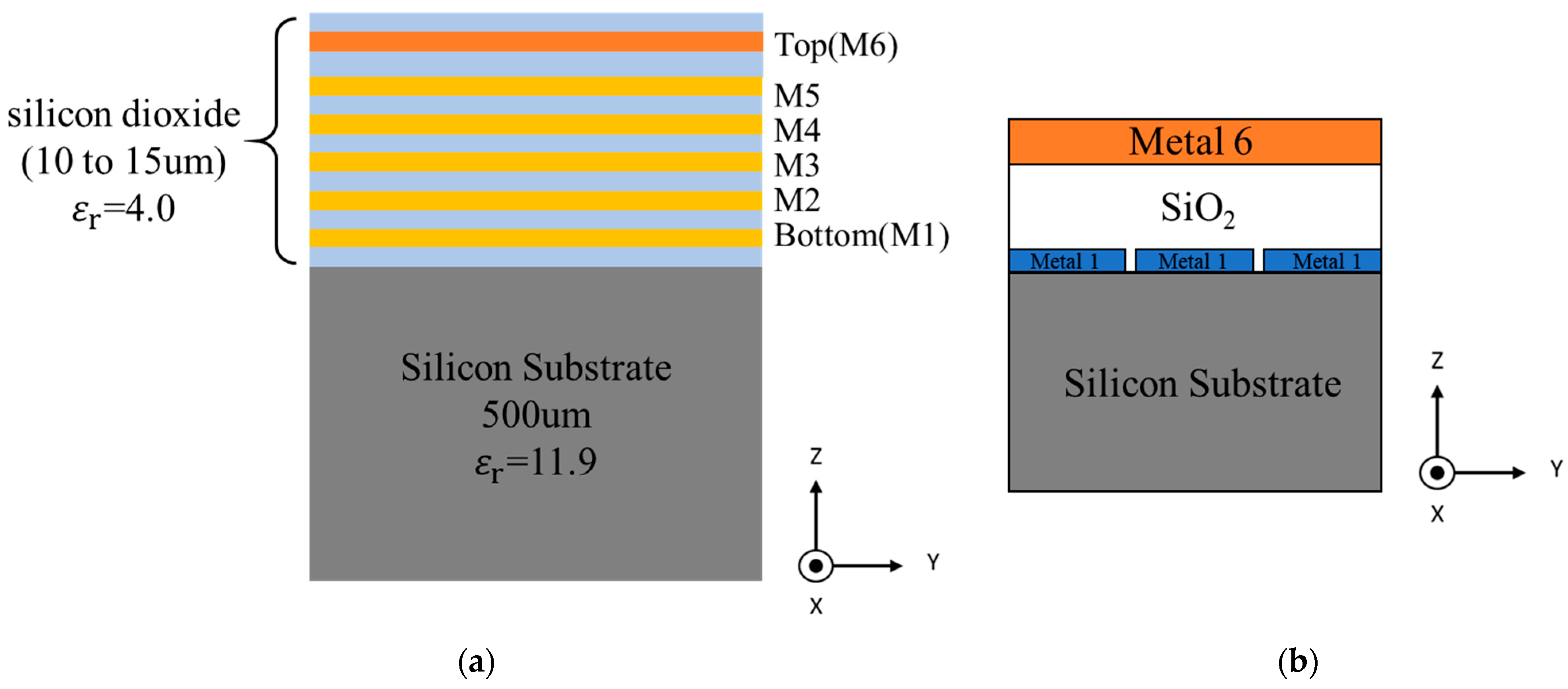
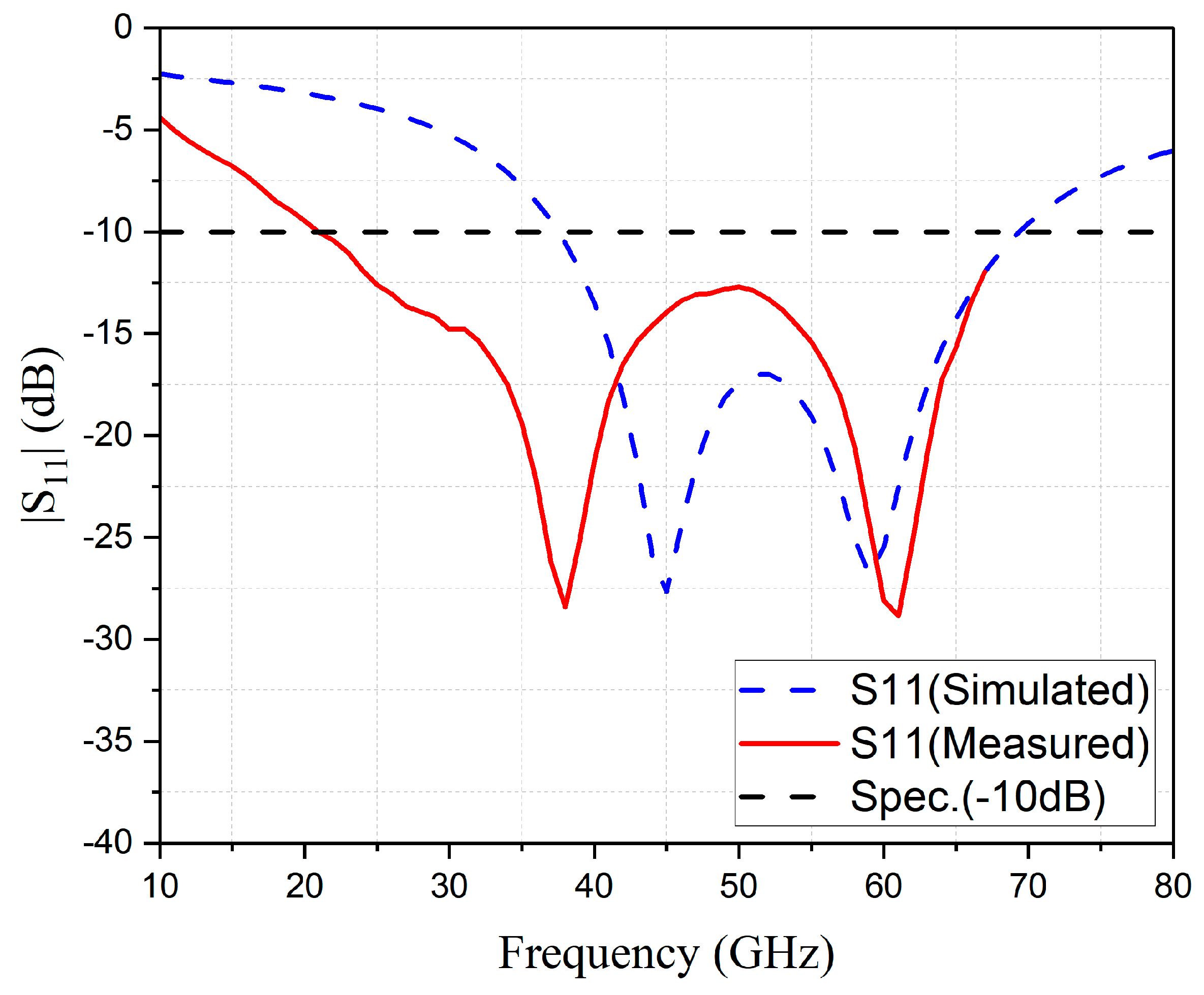
However, the area that can be planned on the top layer of the chip is limited, and how to design an antenna with a high gain and radiation efficiency in the limited area is a big challenge. Therefore, the use of the area needs to be considered when designing the antenna structure, so the antenna type must be carefully selected. For example, the patch antenna [8,15,17,18,19] and Yagi-Uda antenna [22] have a high gain and high directivity, which can make up for the low gain of the antenna-on-chip in terms of performance. This article adopts the structure of the monopole patch antenna to optimize the defects of the chip through the characteristics of high gain and high directivity. The design in this paper adopts TSMC 0.18 μm CMOS process technology, as shown in Figure 1a, which consists of six metal layers (Metal 1 to Metal 6 and the top metal layer) of six layers of silicon dioxide and an Si substrate. In the 0.18 μm CMOS process, the top metal layer (Metal 6) is the designed antenna layer, with a thickness of 2.34 μm, while the thickness of the Si substrate is 500 μm. The antenna design architecture consists of a transmission line and a tapered slit monopole patch antenna and is designed on the top metal layer (Metal 6). The design of AMC on the M1 layer, as shown in Figure 1b, can reduce the loss of electromagnetic waves due to the silicon substrate so that the antenna-on-chip designed in this paper has a better gain and wider application bandwidth. Through the high-frequency electromagnetic simulation software performing full-wave simulation, the antenna-on-chip’s reflection coefficient (S11) is below the −10 dB standard, covering the frequency band from 37.5 GHz to 69.5 GHz, and the fractional bandwidth is 60%. Among them, the bandwidth covers the 38 GHz and 60 GHz application frequency bands of millimeter waves. The antenna has a maximum gain value at 62.1 GHz, exhibiting −2.64 dBi, and was measured at the Taiwan Semiconductor Research Institute of the National Research Institute. The measurement proves that the designed antenna-on-chip has a wider bandwidth. The measured bandwidth is 20.9 to 67 GHz, and the fractional bandwidth is 104.89%. This bandwidth covers the following application frequencies of the millimeter wave: 28 GHz, 38 GHz, and 60 GHz.
2. Structure, Mechanism, and Design
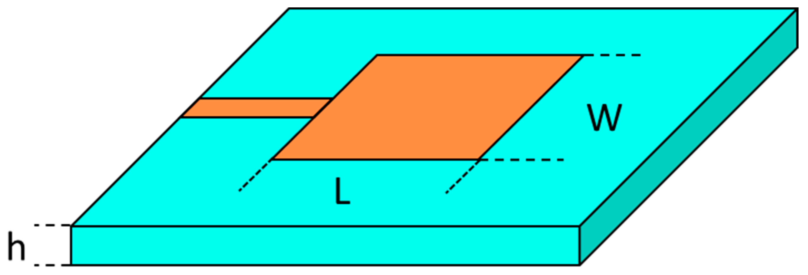
To miniaturize the millimeter wave antenna, the characteristics of a compact size and small assembly components are realized, having performance advantages such as a high gain and high directivity. Figure 2 shows that the patch antenna is the most common design style because of its simple structure. Moreover, structural changes can be designed efficiently for design applications such as cone beams and fan beams, and they are also easy to control.
The following is the basic formula for designing a microstrip patch. The width W of a rectangular patch is obtained by the following Formula (1); the effective dielectric constant can be calculated using (2); the length L is obtained by the following Formula (5):
where W is the width of the patch antenna, is the speed of light, is the dielectric constant of the substrate, is the frequency, is the effective dielectric constant, is the length difference affected by the edge effect, is the effective length, and L is the actual length of the patch antenna.
In addition, the antenna element is fed by a microstrip transmission line with a characteristic impedance of 50 Ω. It can be expressed using Formula (6):
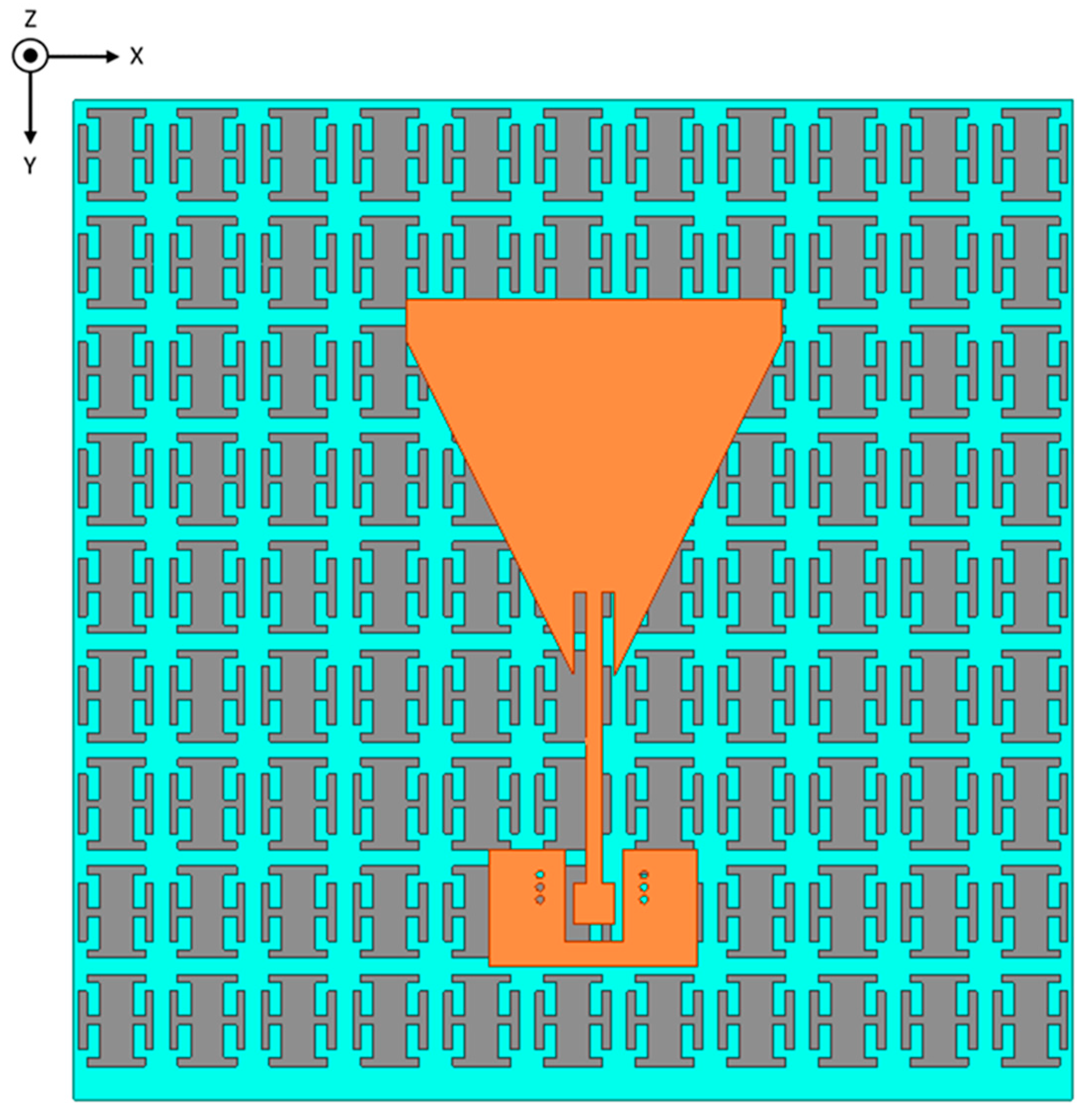
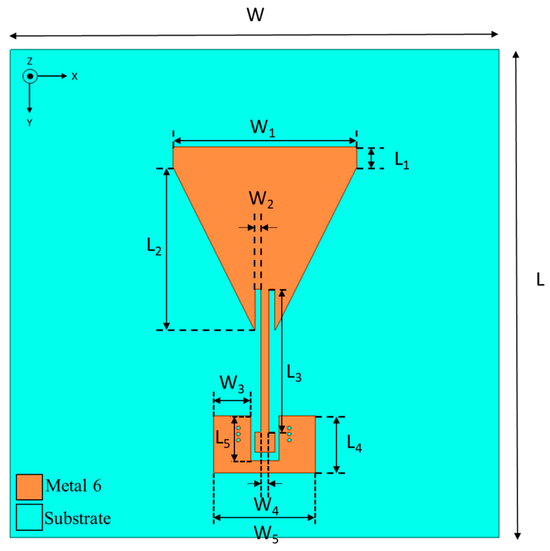
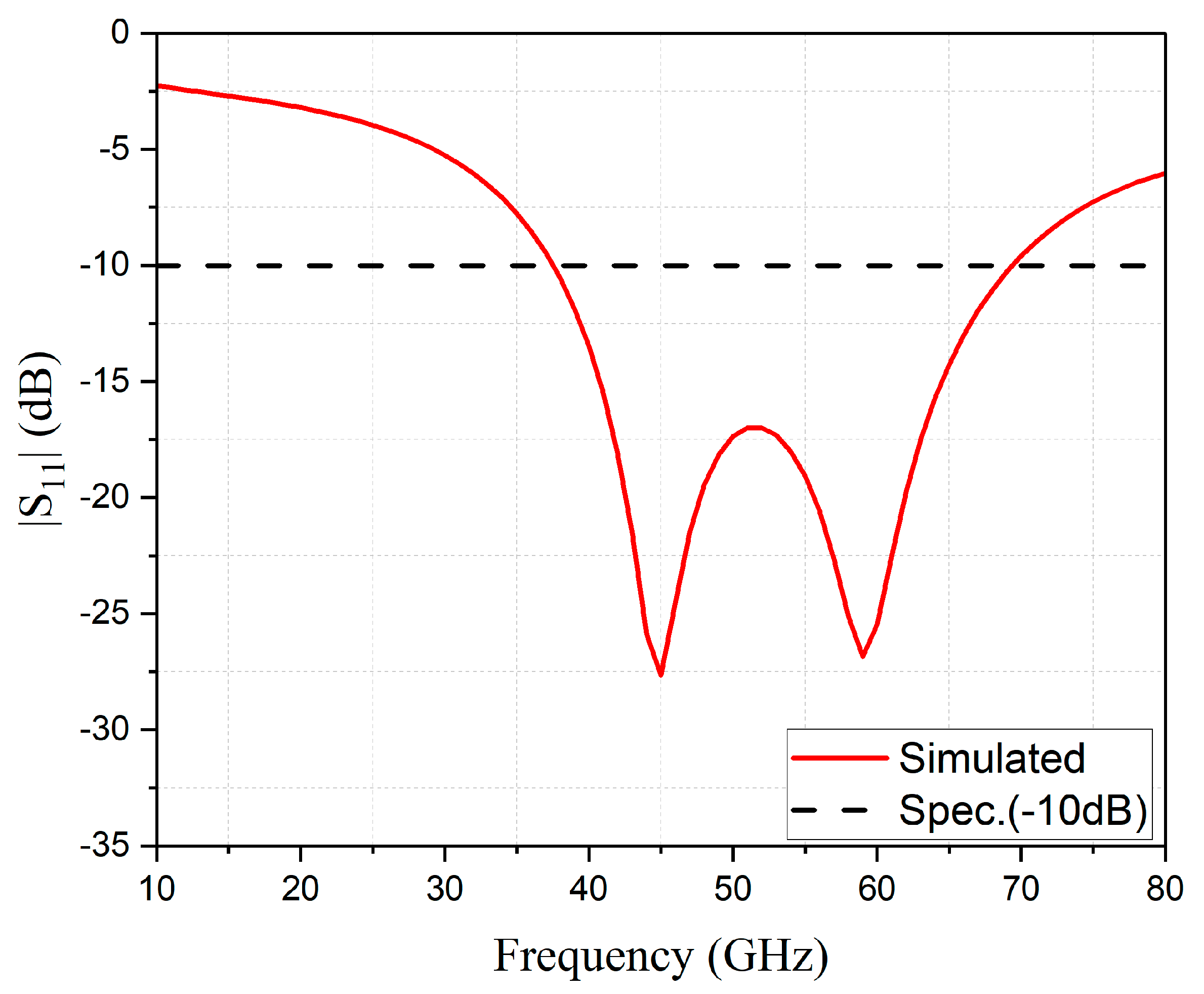
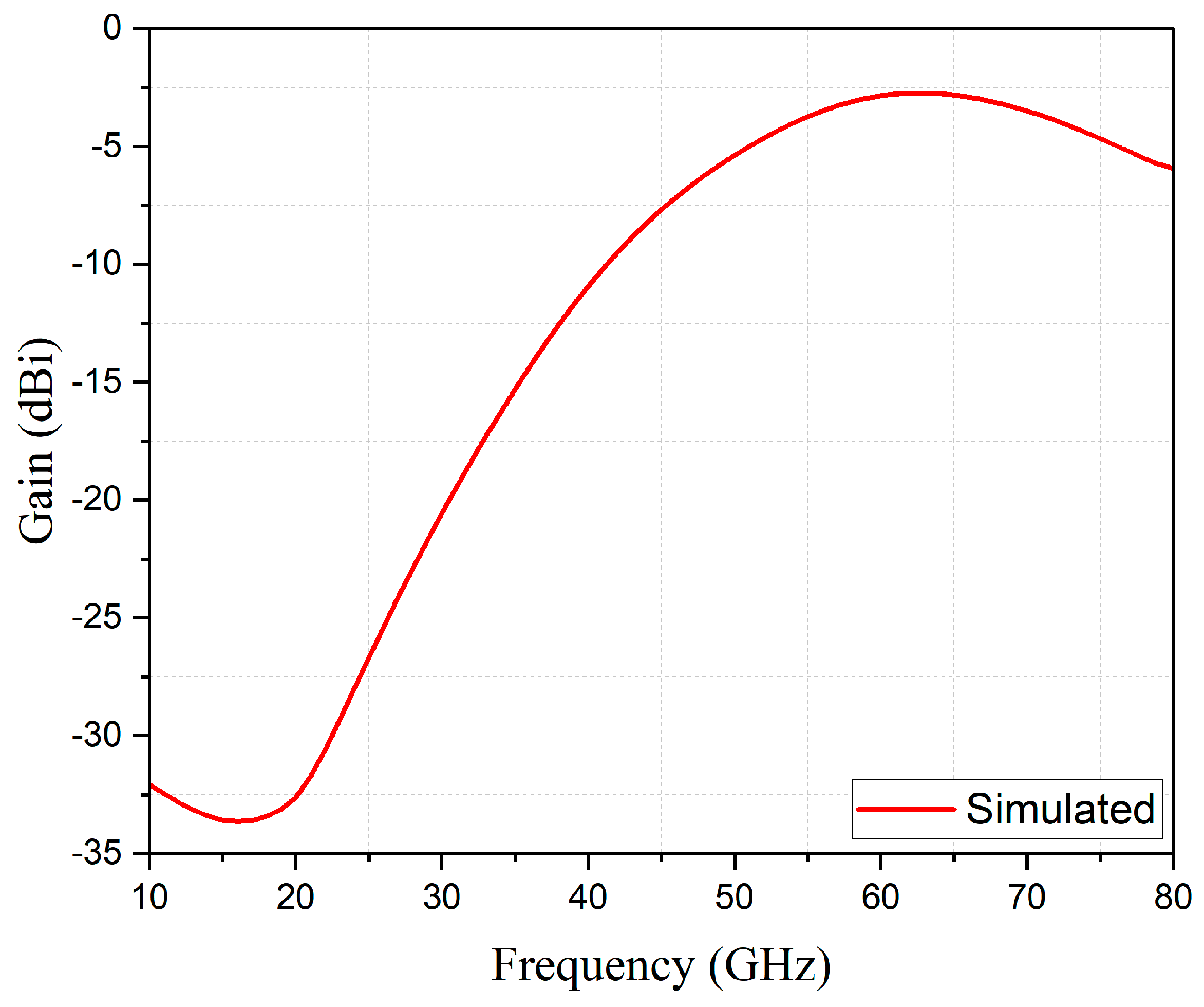
As shown by the above documents, patch antennas have many advantages. Therefore, considering the above documents, this paper designs an antenna-on-chip using TSMC 0.18 μm CMOS process technology, having a high bandwidth in the millimeter wave band. As shown in Figure 3, the overall structure comprises a triangular patch monopole antenna and a transmission line. In addition, the design of the AMC on the M1 layer is designed to enhance the gain of the antenna-on-chip, to prevent electromagnetic waves from spreading to the bottom and damaging the Si substrate, and to reduce the loss of electromagnetic waves [21]. The grounding of the antenna and the transmission line fed into the monopole antenna form a coplanar waveguide (CPW). The radiation gain and direction of the antenna-on-chip can be controlled by adjusting the size of the grounding area to achieve high-gain, high-directivity antenna performance. The geometric size of the antenna-on-chip and the overall size of the chip are marked with parameters, as shown in Figure 4. The values of all parameters are summarized in Table 1. The geometric size and detailed parameter values of the M1-layer AMC single structure are shown in Figure 5 and Table 2 and are simulated by high-frequency electromagnetic simulation software. The simulated reflection coefficient and radiation gain of the antenna-on-chip are shown in Figure 6 and Figure 7. In this simulation, the antenna has the minimum reflection coefficient at 45 GHz, a coverage frequency band from 37.5 GHz to 69.5 GHz, and a maximum gain value of −2.64 dBi at 62 GHz.
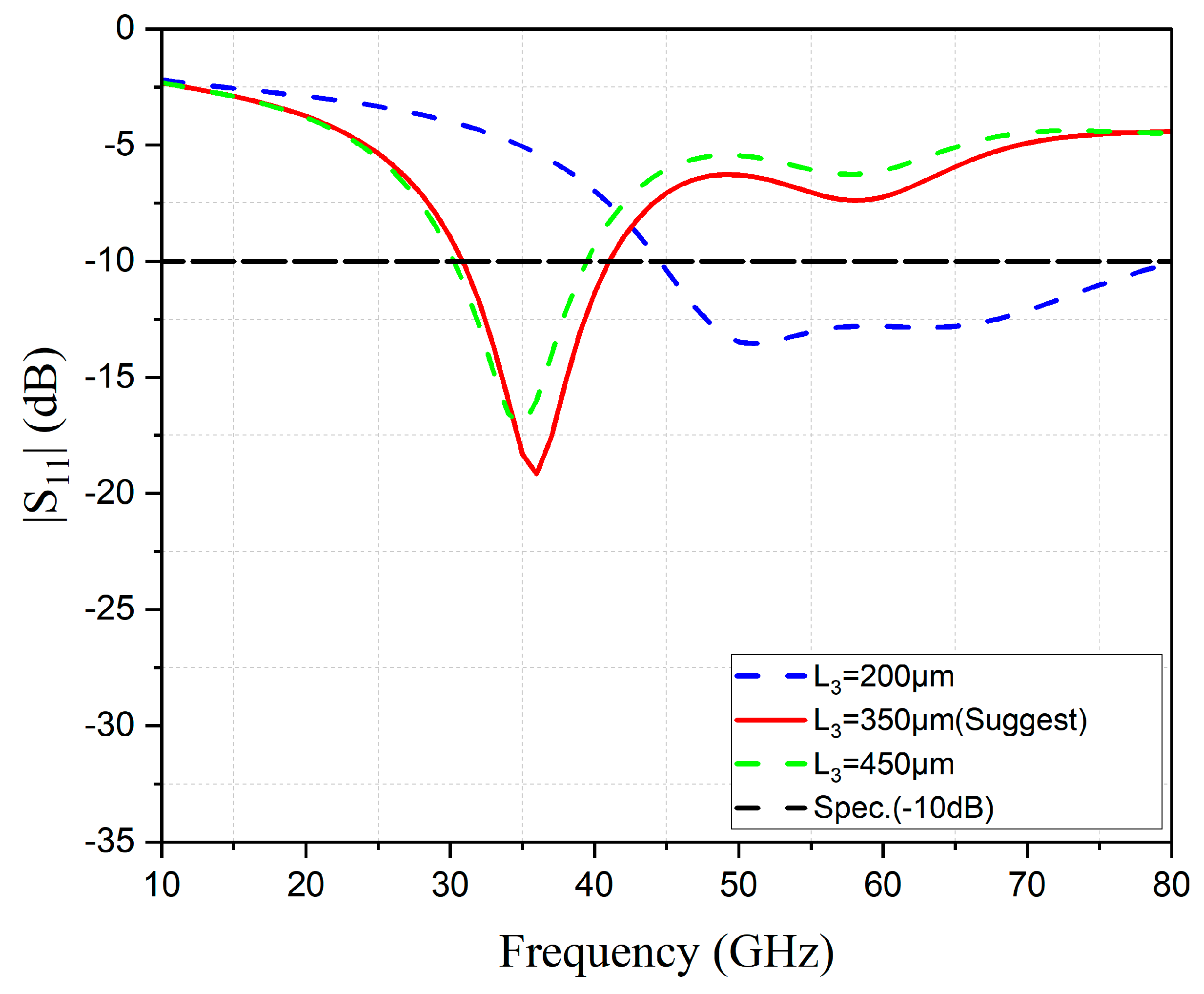
The parameters of the antenna structure designed in this paper are analyzed to obtain the maximum radiation gain. As shown in Figure 8, the length of the feeder transmission line of this antenna structure is analyzed, and the detailed size and bandwidth are shown in Table 3. When the feed-in line length L3 is 200 μm, the frequency bandwidth is 35 GHz when the reflection coefficient of the frequency band is lower than −10 dB, but the minimum reflection coefficient is only −13 dB. Moreover, when the length L3 of the feed line is increased to 350 μm, the bandwidth is 11 GHz when the reflection coefficient of the frequency band is lower than −10 dB, and the minimum value of the reflection coefficient reaches −20 dB. Finally, when the length L3 of the feed-in line increases to 450 μm, the bandwidth is 9 GHz when the reflection coefficient of the frequency band is lower than −10 dB. Therefore, through parameter analysis, the optimal length L3 of the feed-in transmission line can be known, so 350 μm is selected for the length L3 of the feed-in transmission line to obtain the best bandwidth and minimum reflection coefficient.
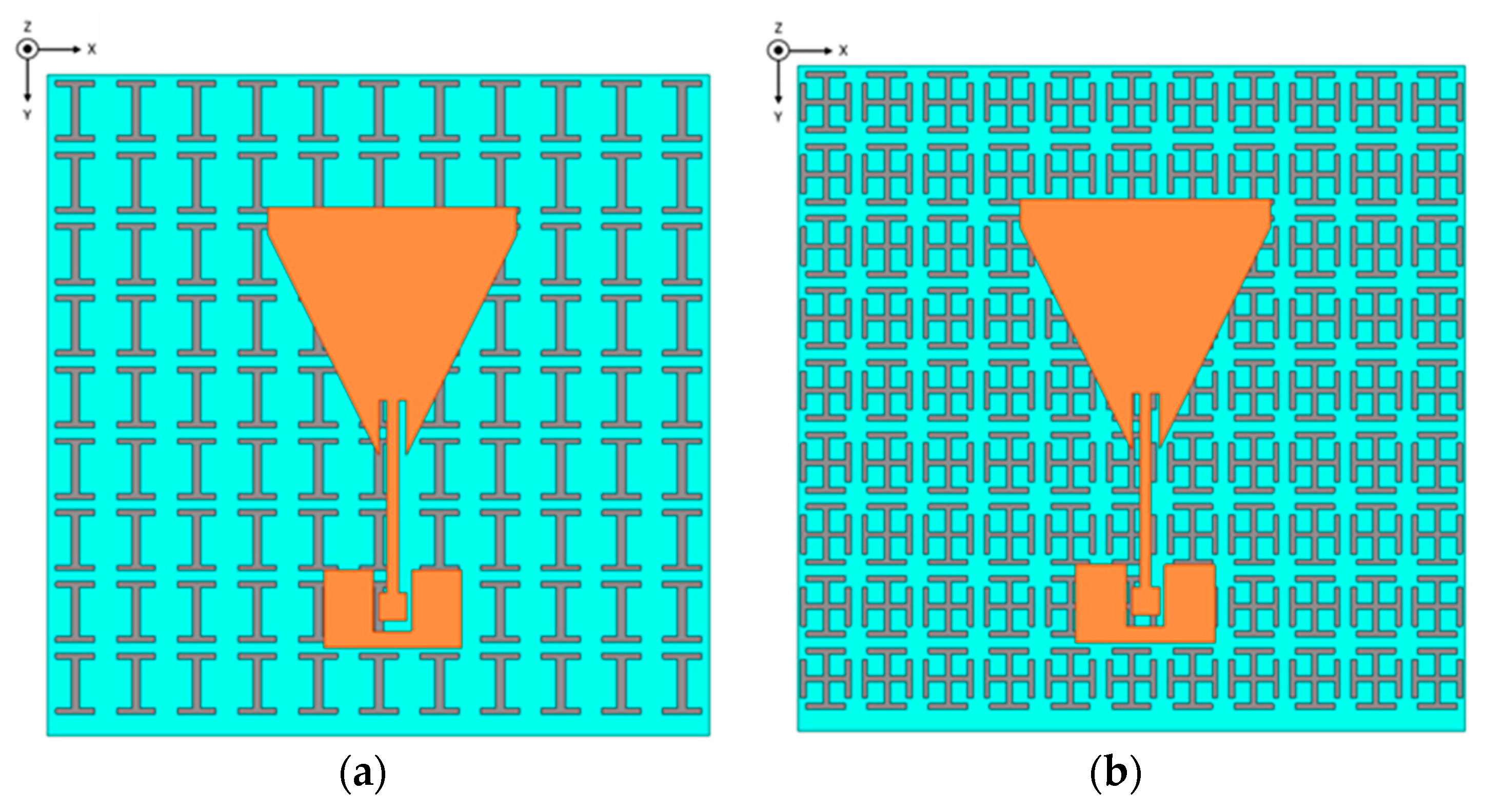
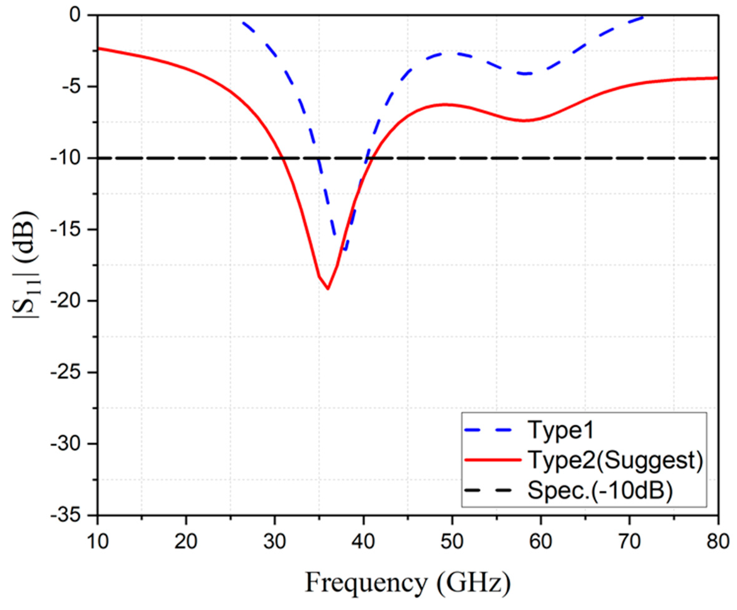
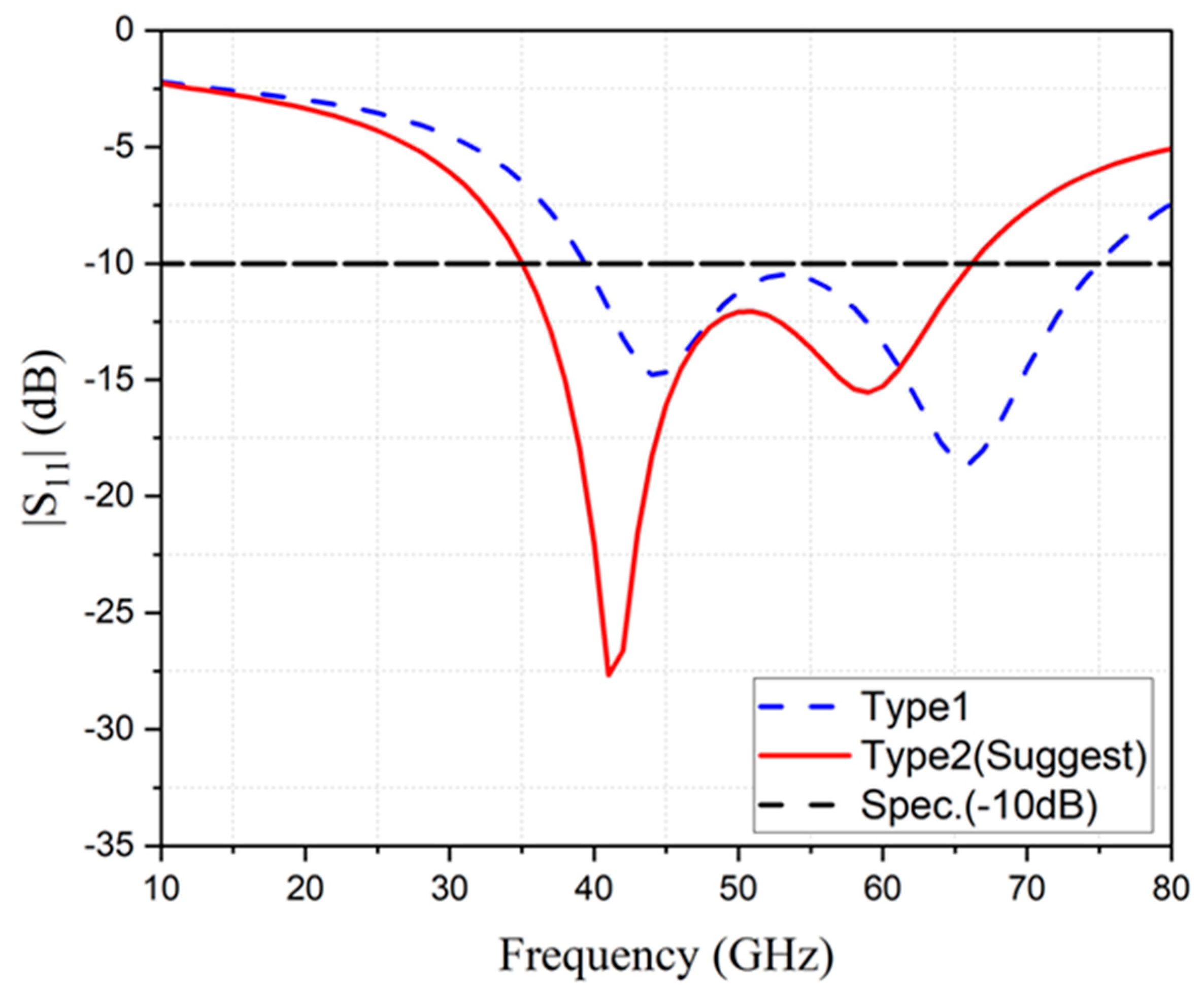
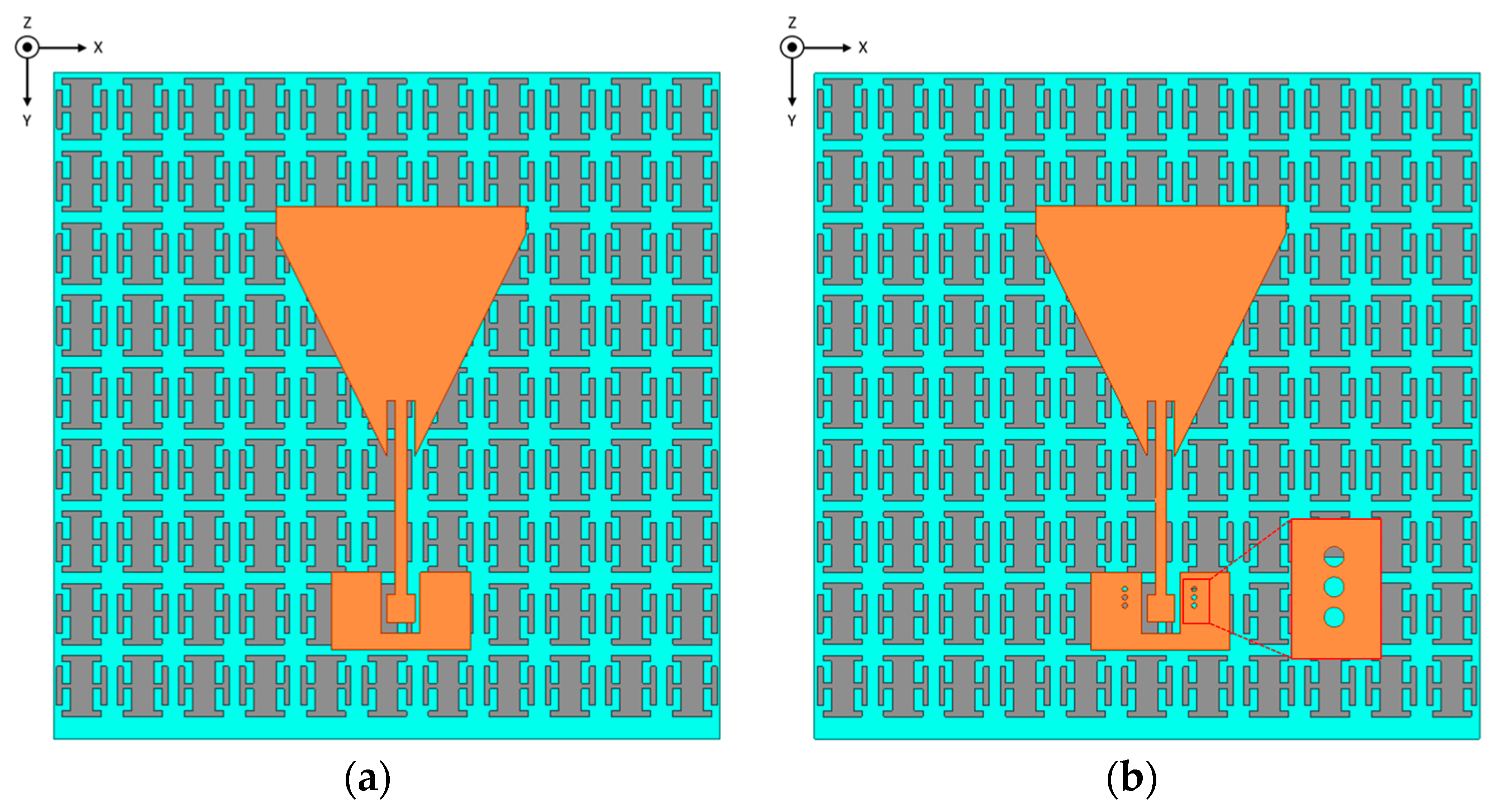
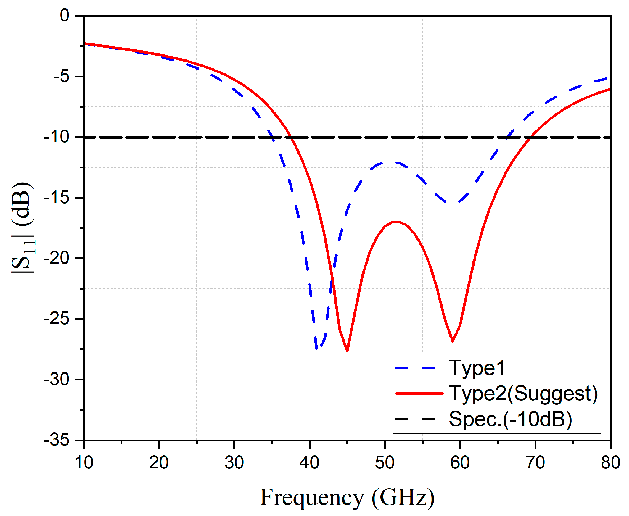
Through parameter analysis, the graphic unit of the M1 layer AMC is designed. It can be seen from Figure 9 that two types of AMCs are designed in this paper, and it can be known that the type of AMC will affect the reflection coefficient (S11) from the Figure 10. In the first type, it can be known that the bandwidth is only 6 GHz under the reflection coefficient standard −10 dB. In the second type, it can be known that, under the reflection coefficient standard −10 dB, a wider bandwidth and a smaller reflection coefficient are obtained. Therefore, the second type in AMC is chosen for the best performance.
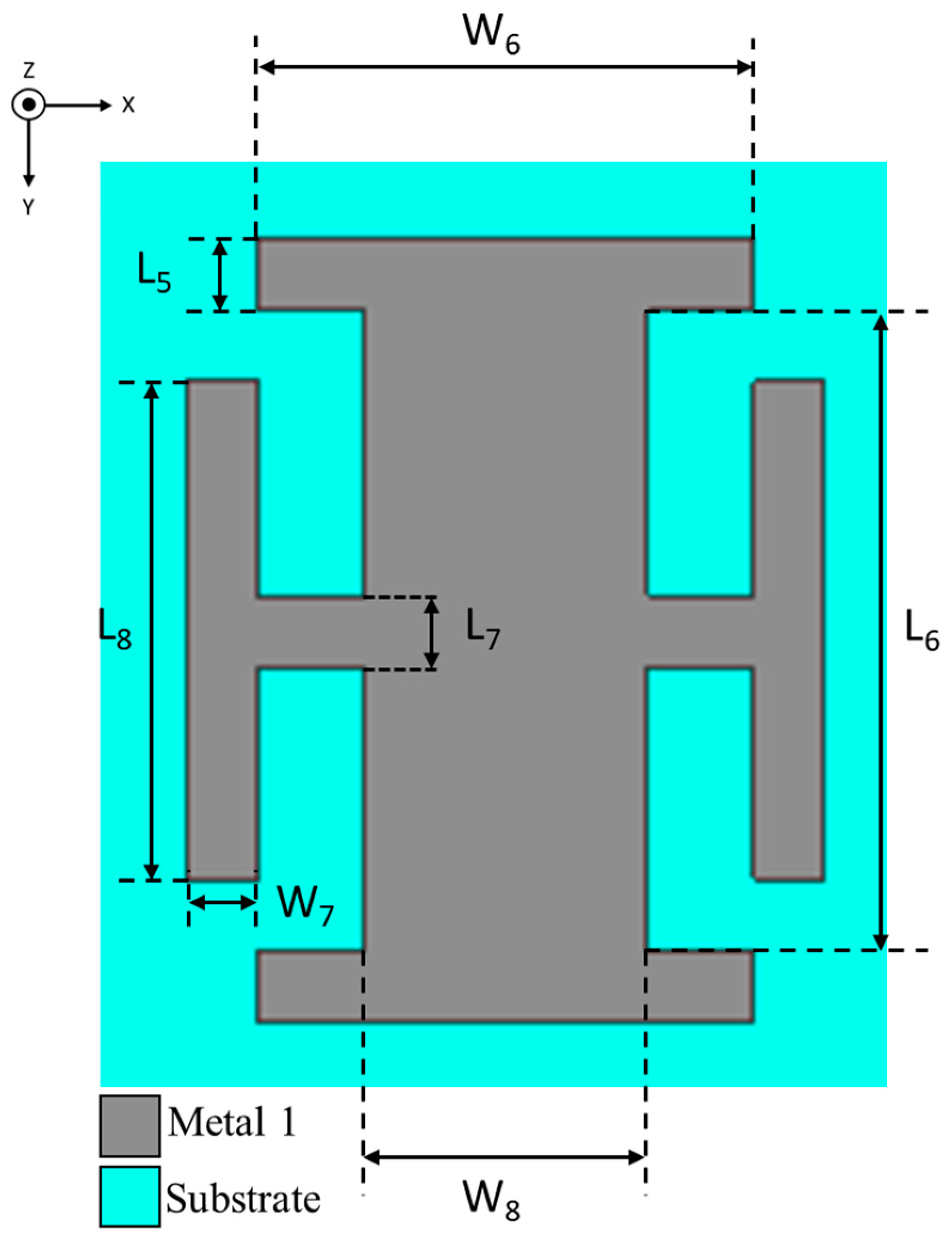
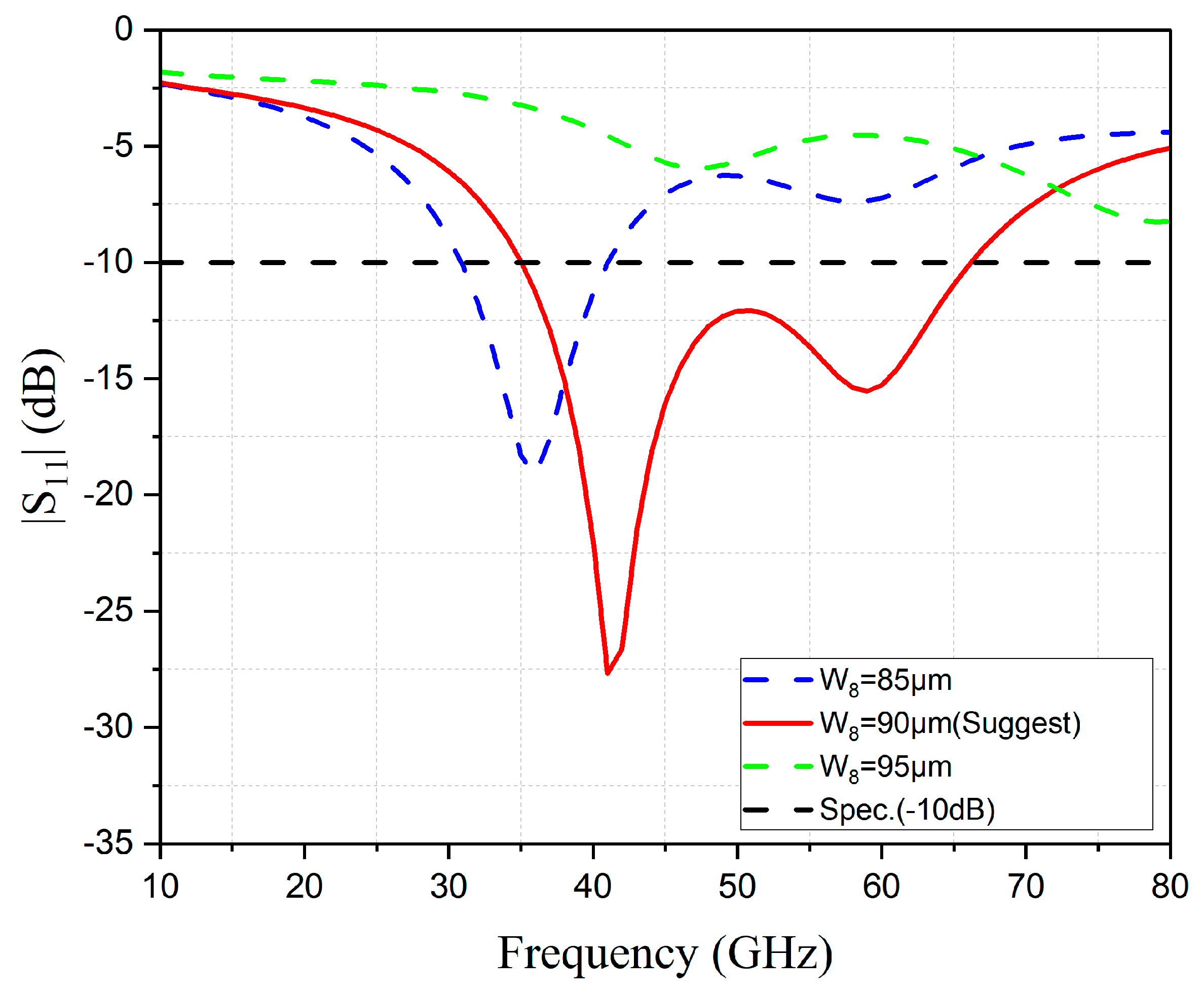
The graphics unit of the M1 layer AMC was analyzed by parametric analysis. It can be known from Figure 11 that the width of the graphic unit pattern will affect the minimum value and bandwidth of the reflection coefficient (S11) in the horizontal structure adjustment of the graphic unit. For example, when the width W8 of the horizontal structure of the unit pattern is 85 μm, it can be known that, under the reflection coefficient standard of −10 dB, the bandwidth has no obvious tendency to become the surface. Furthermore, when the horizontal frame width of the unit pattern is 90 μm, it can be found that, under the reflection coefficient standard −10 dB, it has a wider bandwidth and a minimum reflection coefficient compared to when W8 is 85 μm. However, when the horizontal width of the unit pattern reaches 95 μm, it can already be found that the reflection coefficient cannot reach the standard value of −10 dB. Therefore, the lateral structure width of the graphic unit of the AMC of the M1 layer is selected to be 90 μm to obtain the best performance.
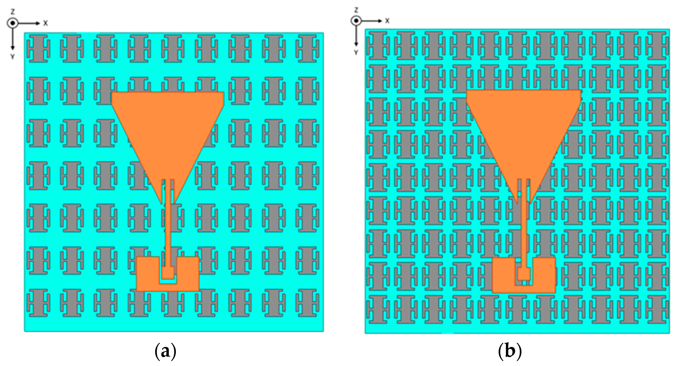
The AMC with different periodic array sizes is analyzed, as shown in Figure 12. For example, it can be seen from Figure 13 that, in the AMC with a regular array size of 7 × 9, it can be known that the minimum reflection coefficient (S11) is −18 dB. On the other hand, in an AMC with a regular array size of 9 × 11, its bandwidth is 31 GHz, with a minimum reflection coefficient (S11) of −27 dB at a standard reflection coefficient of −10 dB. Therefore, an AMC with a regular array size of 9 × 11 is chosen.
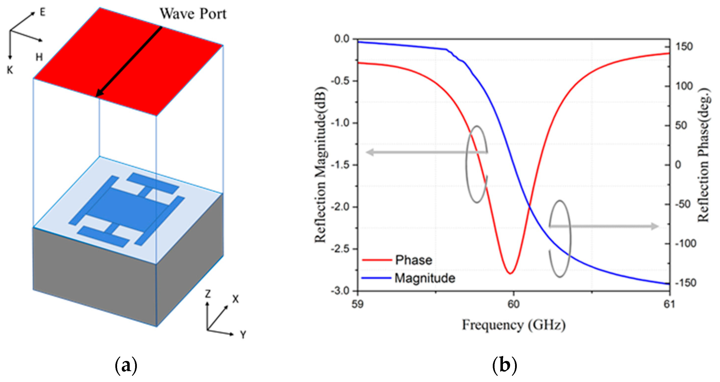
Next, the reflection phase of AMC in the M1 layer is analyzed. Figure 14a is the AMC unit model designed in this paper. It can be known from Figure 14b that the AMC designed in this paper has a phase bandwidth and a high reflection coefficient at an operating frequency of 60 GHz.
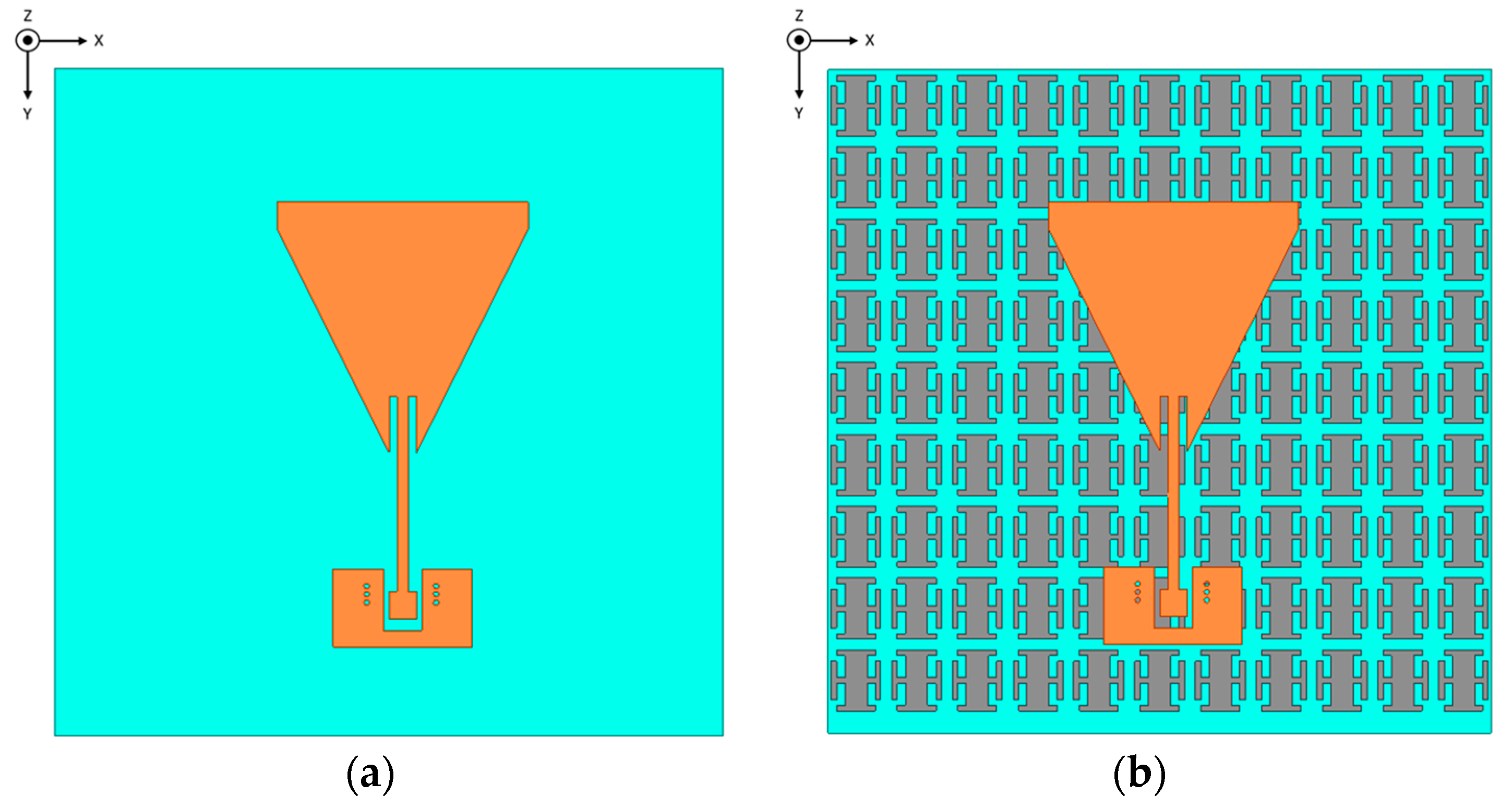
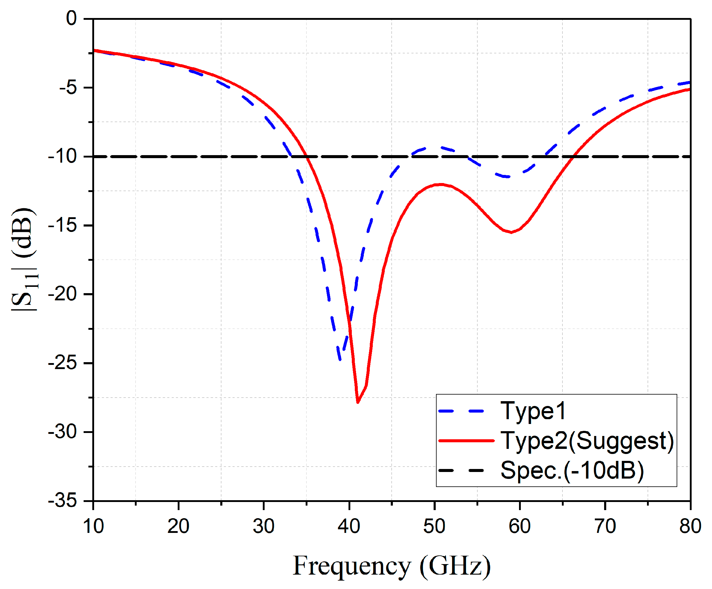
In Figure 15, parameter analysis is also performed through the presence or absence of M1 AMC. Figure 16 shows that when the AMC is designed with the M1 layer, a lower value of the reflection coefficient (S11) can be obtained. However, when AMC is designed without the M1 layer, the bandwidth cannot continuously reach the standard −10 dB of the reflection coefficient. Therefore, by comparing the simulations, it is possible to analyze the influence on the reflection coefficient of the antenna when designing the AMC with or without the M1 layer.
In terms of probe GSG grounding, as shown in Figure 17, in this paper, a circular hole is drilled in the probe grounding area, and the simulation diagram is shown in Figure 18. When the probe GSG grounding area has no holes, and the frequency is 60 GHz, the minimum reflection coefficient is only −14 dB, and the bandwidth is 31 GHz. Then, through the penetration method of the hole in the GSG grounding area, impedance matching is achieved so that the 60 GHz frequency band can reach the standard reflection coefficient of −10 dB, the minimum reflection coefficient can reach −26 dB, and the bandwidth can reach 32 GHz.
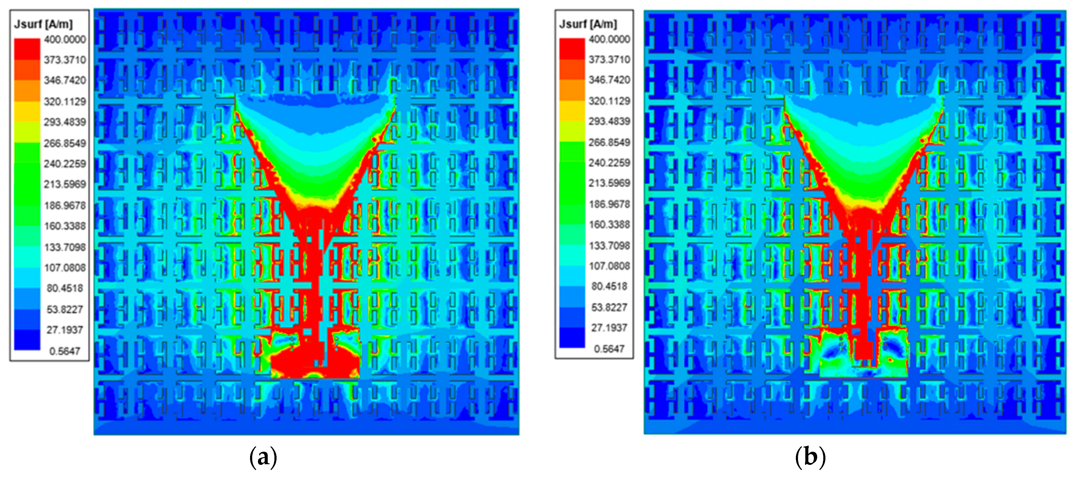
As shown in Figure 19, this paper analyzes the antenna’s architectural operation through the current distribution. The antenna designed in this paper uses the probe GSG method to feed the signal, which excites the antenna body to generate the surface current. The current is distributed to the antenna body through the CPW structure of the feeding line. Figure 19a,b show the current distribution state at 38 and 60 GHz. In the 34 GHz to 65 GHz frequency band, the area where the current distribution is more obvious is the area of the tapered patch and its surrounding area. It can be judged that the resonance of the tapered patch antenna generates this frequency band.
3. Results
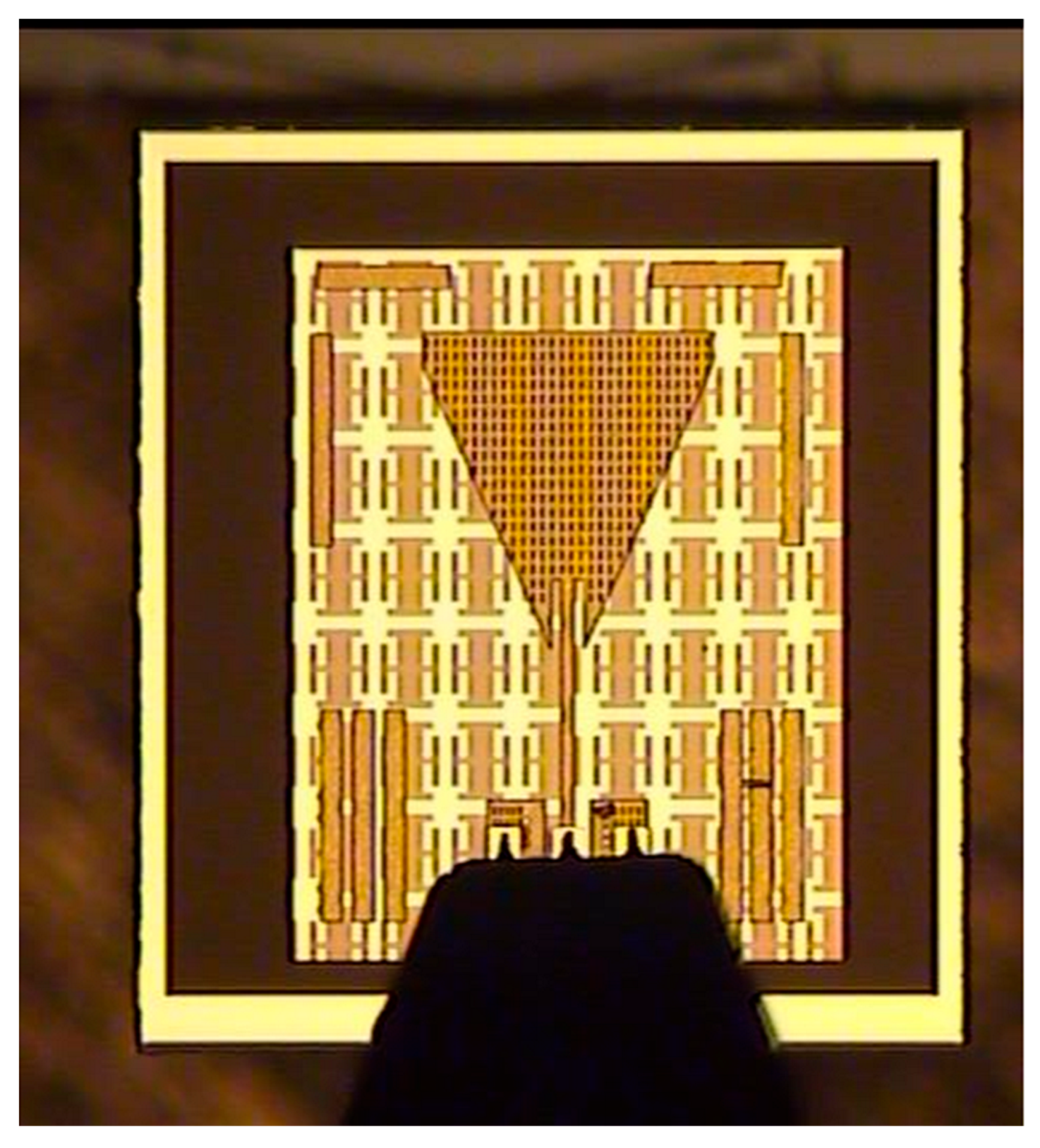
Figure 20 shows the antenna–on-chip designed in this paper, using the GSG probe to perform needle insertion and using the large magnification to measure frontal photos. The measured reflection coefficient (S11) of the antenna designed in this paper was measured at the Taiwan Semiconductor Research Institute of the National Research Institute (Taiwan Semiconductor Research Institute), using a vector network analyzer (Agilent E8361C) as the feed system and using a spacing of 100 μm; the GSG probe transmits signals for the antenna. Figure 21 shows the simulation and measurement results of the millimeter wave band antenna-on-chip designed in this experiment, which have the same trend. However, the difference between the position of the GSG probe and the simulation during the measurement affects the bandwidth result of the measurement, and the bandwidth under the standard reflection coefficient of −10 dB has a higher application frequency than the simulation, covering millimeter wave application frequencies of 28 GHz, 38 GHz, and 60 GHz. The measurement results after the frequency of 67 GHz are unknown, but it can be inferred from the previous measurement trend that the measurement results will be similar to those of the simulation.
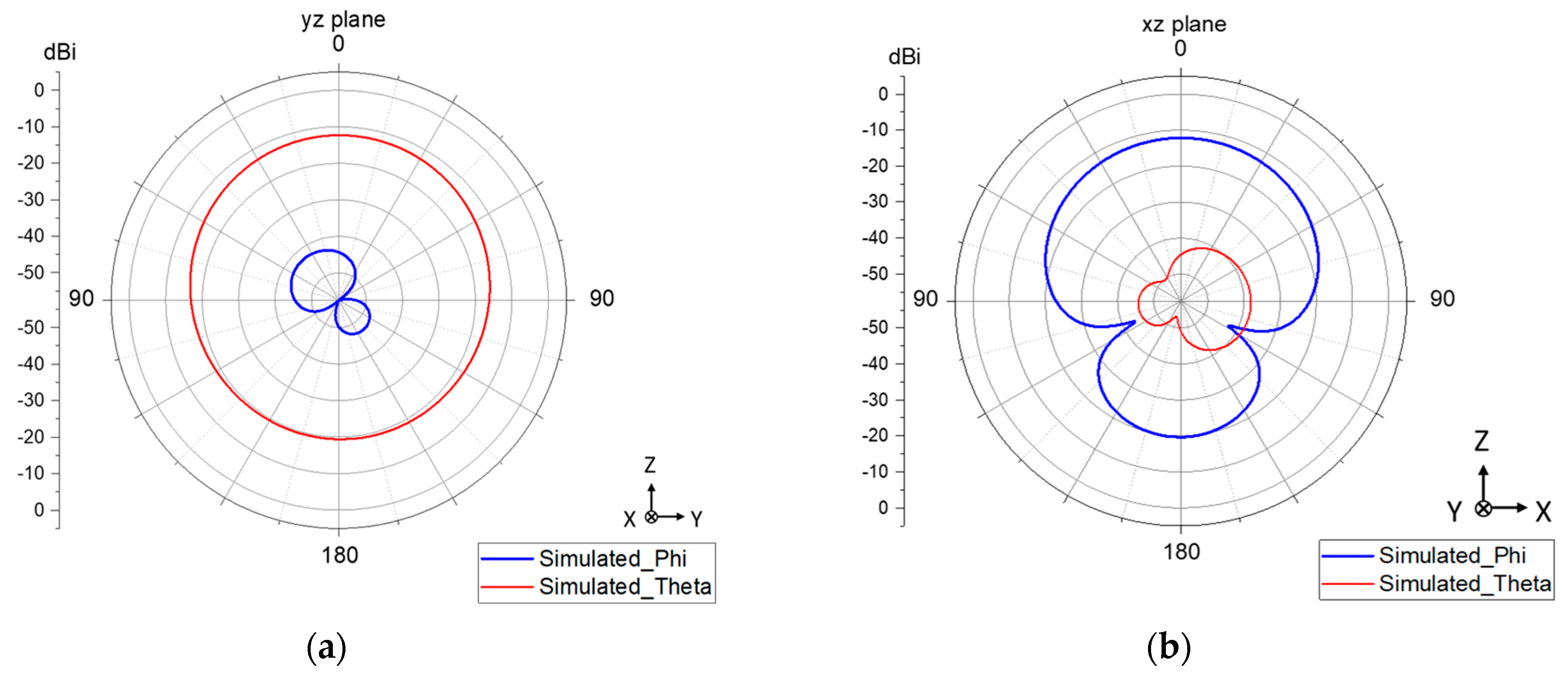
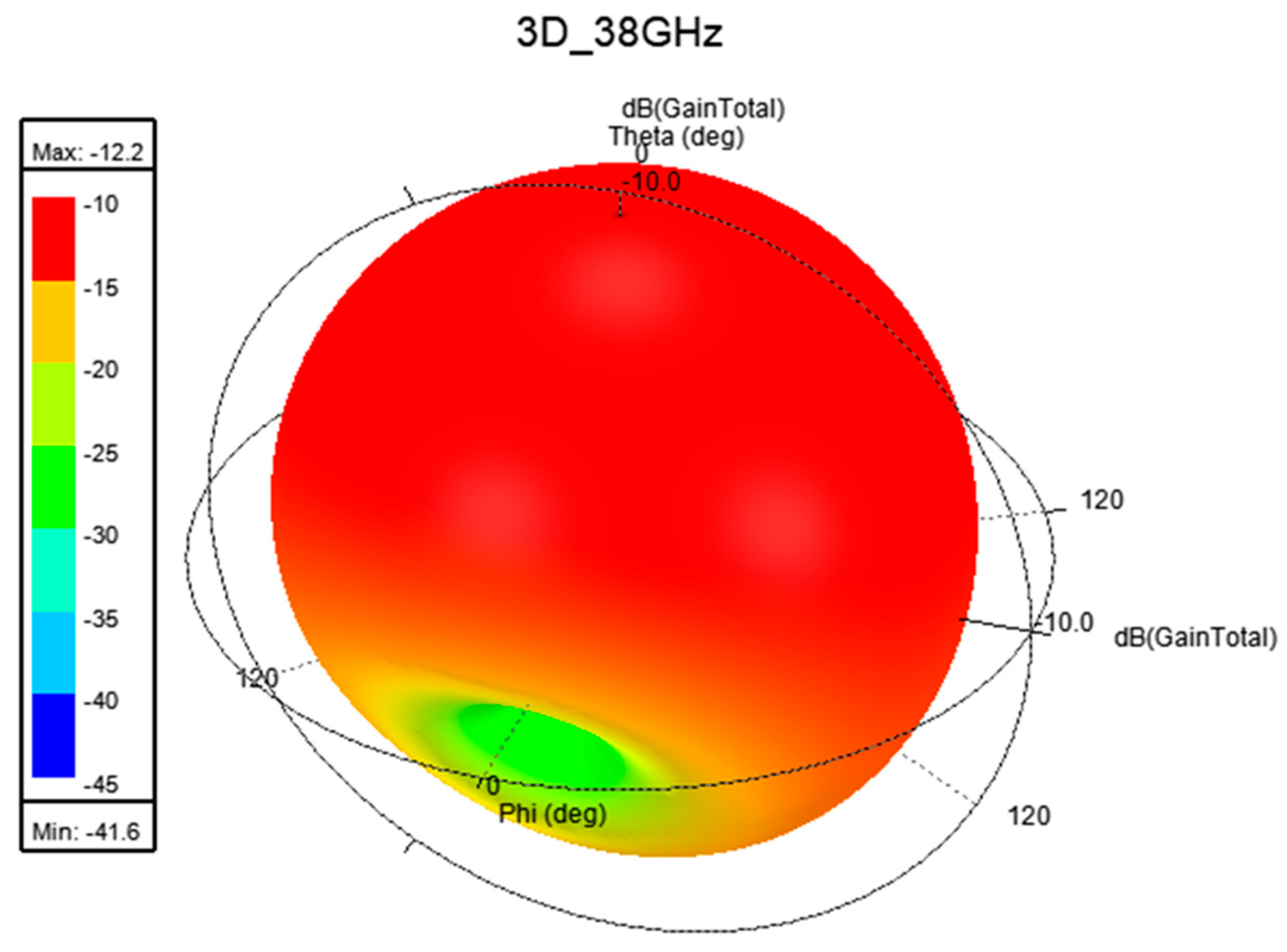
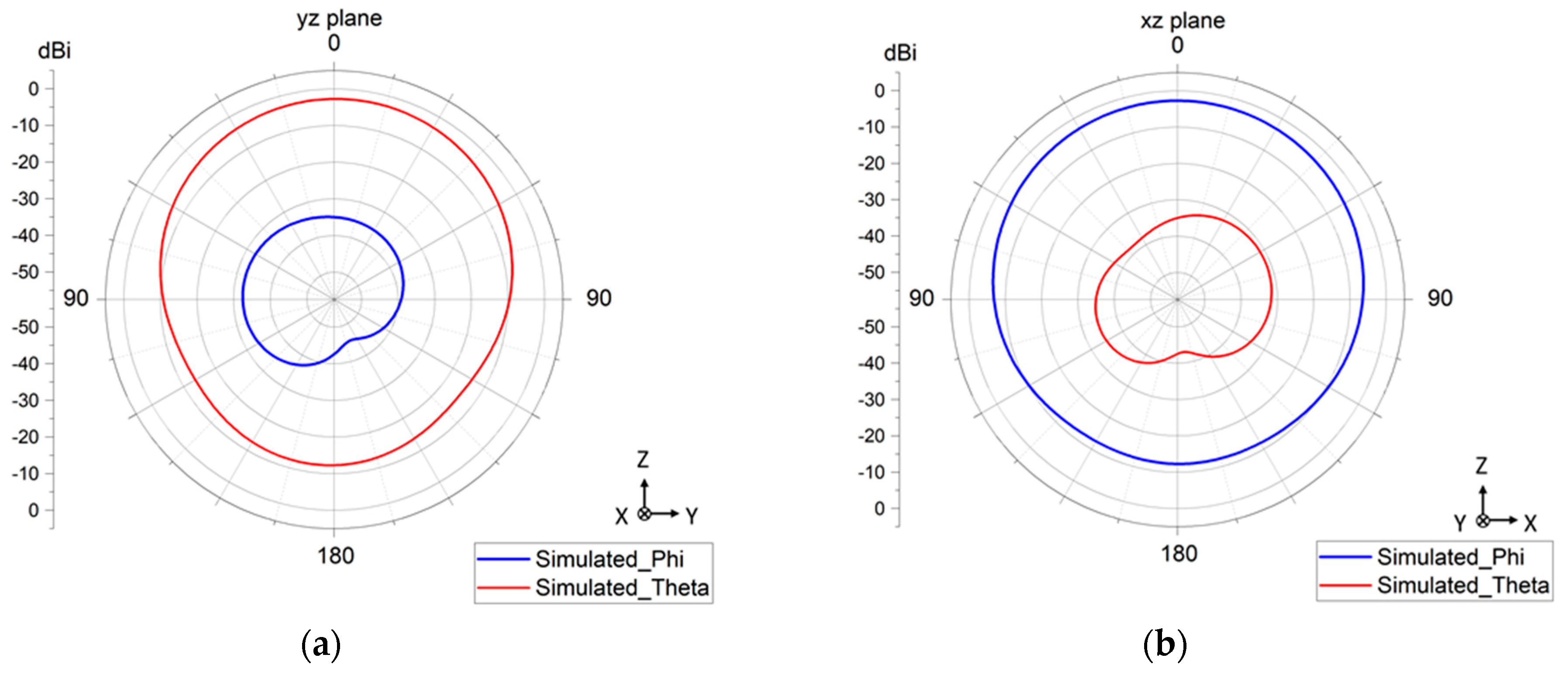
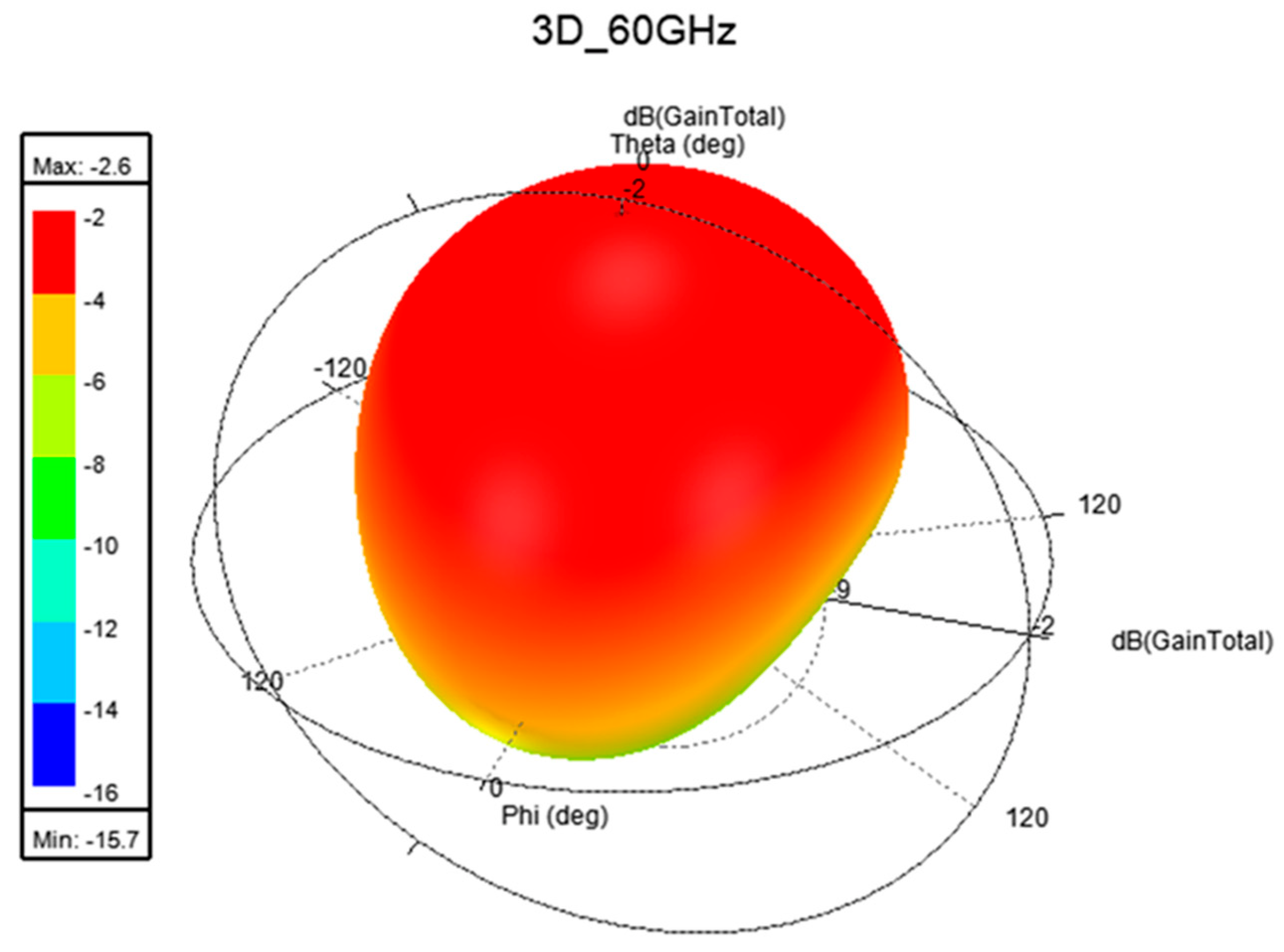
This paper simulated the radiation direction through high-frequency electromagnetic simulation software regarding the antenna radiation pattern. Through the 2D field pattern, the radiation directions in the xz and yz planes can be analyzed, and the radiation directions of the chip antenna designed in this document at 38 GHz and 60 GHz can be better understood. Figure 22 and Figure 23 are the 2D plane field radiation diagram and the 3D field radiation diagram of 38 GHz. When the theta angle is 1 degree, the maximum gain is −12.2 dBi. The xz plane field radiation diagram shows that when the Theta angle is 2 degrees, the maximum gain is −12 dBi. Figure 24 and Figure 25 are 2D planar field radiation diagrams and 3D field radiation diagrams of 60 GHz. It can be known that when the theta angle is 2 degrees, the maximum gain is −2.64 dBi. The xz plane field radiation diagram shows that when the theta angle is 2 degrees, the maximum gain is −2.56 dBi. According to the above xz, yz plane radiation pattern simulation diagram and 3D radiation simulation diagram, it can be known that the radiation pattern of this antenna is upward, and the maximum gain is −2.64 dBi.
4. Discussion
From the above parameter simulation, it can be known that the grounding part of GSG can achieve impedance matching through our hole design so that the design frequency band can reach the standard reflection coefficient of −10 dB and achieve a smaller value of reflection coefficient (S11). By designing AMC in the M1 layer, the antenna-on-chip can achieve a better performance and widen the bandwidth. Coupled with the advantages of the high gain and high directivity of the patch antenna, it can complement the lack of performance of the antenna-on-chip. As shows in Table 4, the measurement results of the antenna designed in this paper are more comprehensive than the bandwidth of the literature [8,9,15,17,18,19,20,21,22,23] and have more and broader bandwidth application advantages. In terms of gain, it has a more significant gain value than those in the literature [17,23]. Furthermore, the area part is smaller than the area used in the literature [18,20], using a smaller area to achieve a broader bandwidth.
5. Conclusions
This paper proposes a monopole patch antenna, and AMC is designed in the M1 layer. Through simulation analysis, it can be known that, without AMC, the antenna bandwidth designed in this paper cannot be lower than the standard reflection coefficient of −10 dB. The design of AMC achieves the minimum reflection coefficient, and the designed bandwidth is lower than the standard reflection coefficient standard of −10 dB. In simulations, the bandwidth ranges from 34 to 65 GHz, with a fractional bandwidth of 104%. At 62 GHz, a maximum radiation benefit value of −2.64 dB is obtained. The measurement obtained a larger bandwidth covering 20.9 GHz to 67 GHz, with a fractional bandwidth of 104.89%. The method proposed in this paper can improve the influence of the antenna-on-chip caused by the CMOS process and can obtain more of a radiation gain and a lower reflection coefficient (S11). As a result, future millimeter wave antennas can be implemented on chips, making the antennas compact and less susceptible to external factors while still having a good radiation gain and efficiency.
Author Contributions
Conceptualization, M.-A.C.; methodology, M.-A.C.; software, M.-A.C. and I.-P.M.; validation, M.-A.C., Y.-H.C. and I.-P.M.; formal analysis, M.-A.C., Y.-H.C. and I.-P.M.; investigation, Y.-H.C. and I.-P.M.; resources, M.-A.C.; writing—original draft preparation, M.-A.C. and Y.-H.C.; writing—review and editing, M.-A.C.; visualization, M.-A.C.; supervision, M.-A.C.; project administration, M.-A.C.; funding acquisition, M.-A.C. All authors have read and agreed to the published version of the manuscript.
Funding
This research received no external funding.
Data Availability Statement
All data are included within the manuscript.
Conflicts of Interest
The authors declare no conflict of interest.
References
- Li, M.; Zhang, F.; Ji, Y.; Fan, W. Virtual Antenna Array with Directional Antennas for Millimeter-Wave Channel Characterization. IEEE Trans. Antennas Propag. 2022, 70, 6992–7003. [Google Scholar] [CrossRef]
- Sun, Y.-X.; Leung, K.W.; Lu, K. Compact dual microwave/millimeter-wave planar shared-aperture antenna for vehicle-to-vehicle/5G communications. IEEE Trans. Veh. Technol. 2021, 70, 5071–5076. [Google Scholar] [CrossRef]
- Yaduvanshi, R.S. Terahertz Dielectric Resonator Antennas for High Speed Communication and Sensing: From Theory to Design and Implementation; IET: Stevenage, UK, 2021; Volume 103. [Google Scholar]
- Sun, G.-H.; Wong, H. A planar millimeter-wave antenna array with a pillbox-distributed network. IEEE Trans. Antennas Propag. 2020, 68, 3664–3672. [Google Scholar] [CrossRef]
- Tong, X.; Jiang, Z.H.; Yu, C.; Wu, F.; Xu, X.; Hong, W. Low-Profile, Broadband, Dual-Linearly Polarized, and Wide-Angle Millimeter-Wave Antenna Arrays for Ka-Band 5G Applications. IEEE Antennas Wirel. Propag. Lett. 2021, 20, 2038–2042. [Google Scholar] [CrossRef]
- Le Zhang, Q.; Chen, B.J.; Chan, K.F.; Chan, C.H. High-gain millimeter-wave antennas based on spoof surface plasmon polaritons. IEEE Trans. Antennas Propag. 2020, 68, 4320–4331. [Google Scholar] [CrossRef]
- Yu, Y.; Jiang, Z.H.; Zhang, J.-D.; Wu, W. Broadband Millimeter-Wave Endfire Circularly Polarized Array With a Low-Profile Feeding Structure. IEEE Trans. Antennas Propag. 2022, 70, 7270–7275. [Google Scholar] [CrossRef]
- Chung, M.-A.; Lin, C.-W.; Lo, W.-J. Near Field Sensing Applications with Tunable Beam Millimeter Wave Antenna Sensors in an All-in-One Chip Design. Electronics 2022, 11, 2231. [Google Scholar] [CrossRef]
- Burasa, P.; Djerafi, T.; Wu, K. A 28 GHz and 60 GHz dual-band on-chip antenna for 5G-compatible IoT-served sensors in standard CMOS process. IEEE Trans. Antennas Propag. 2020, 69, 2940–2945. [Google Scholar] [CrossRef]
- Liu, Q.; van den Biggelaar, A.; Johannsen, U.; van Beurden, M.C.; Smolders, A.B. On-chip metal tiling for improving grounded mm-Wave antenna-on-chip performance in standard low-cost packaging. IEEE Trans. Antennas Propag. 2019, 68, 2638–2645. [Google Scholar] [CrossRef]
- Althuwayb, A.A.; Alibakhshikenari, M.; Virdee, B.S.; Benetatos, H.; Falcone, F.; Limiti, E. Antenna on chip (AoC) design using metasurface and SIW technologies for THz wireless applications. Electronics 2021, 10, 1120. [Google Scholar] [CrossRef]
- Karim, R.; Iftikhar, A.; Ramzan, R. Performance-Issues-Mitigation-Techniques for On-Chip-Antennas–Recent Developments in RF, MM-Wave, and THz Bands with Future Directions. IEEE Access 2020, 8, 219577–219610. [Google Scholar] [CrossRef]
- Gutierrez, F.; Agarwal, S.; Parrish, K.; Rappaport, T.S. On-chip integrated antenna structures in CMOS for 60 GHz WPAN systems. IEEE J. Sel. Areas Commun. 2009, 27, 1367–1378. [Google Scholar] [CrossRef]
- Zhu, H.; Li, X.; Feng, W.; Xiao, J.; Zhang, J. 235 GHz on-chip antenna with miniaturised AMC loading in 65 nm CMOS. IET Microw. Antennas Propag. 2018, 12, 727–733. [Google Scholar] [CrossRef]
- Hedayati, M.K.; Abdipour, A.; Shirazi, R.S.; Ammann, M.J.; John, M.; Cetintepe, C.; Staszewski, R.B. Challenges in on-chip antenna design and integration with RF receiver front-end circuitry in nanoscale CMOS for 5G communication systems. IEEE Access 2019, 7, 43190–43204. [Google Scholar] [CrossRef]
- Kong, S.; Shum, K.M.; Yang, C.; Gao, L.; Chan, C.H. Wide impedance-bandwidth and gain-bandwidth terahertz on-chip antenna with chip-integrated dielectric resonator. IEEE Trans. Antennas Propag. 2021, 69, 4269–4278. [Google Scholar] [CrossRef]
- Gaha, H.I.; Balti, M. Novel Bi-UWB on-Chip Antenna for Wireless NoC. Micromachines 2022, 13, 231. [Google Scholar] [CrossRef]
- Mustacchio, C.; Boccia, L.; Arnieri, E.; Amendola, G. A gain levelling technique for on-chip antennas based on split-ring resonators. IEEE Access 2021, 9, 90750–90756. [Google Scholar] [CrossRef]
- Zhu, C.; Duan, Z.; Ma, Q. 94-GHz CMOS on-Chip Antenna Based on Stacked Dielectric Resonators and Substrate Integrated Waveguide Multi-Feed Network. In Proceedings of the 2021 46th International Conference on Infrared, Millimeter and Terahertz Waves (IRMMW-THz), Chengdu, China, 29 August–3 September 2021; pp. 1–3. [Google Scholar]
- Burasa, P.; Djerafi, T.; Constantin, N.G.; Wu, K. On-chip dual-band rectangular slot antenna for single-chip millimeter-wave identification tag in standard CMOS technology. IEEE Trans. Antennas Propag. 2017, 65, 3858–3868. [Google Scholar] [CrossRef]
- Khan, M.S.; Tahir, F.A.; Meredov, A.; Shamim, A.; Cheema, H.M. A W-band EBG-backed double-rhomboid bowtie-slot on-chip antenna. IEEE Antennas Wirel. Propag. Lett. 2019, 18, 1046–1050. [Google Scholar] [CrossRef]
- Sultan, K.S.; Abdallah, E.A.; El Hennawy, H. A multiple-input-multiple-output on-chip Quasi-Yagi-Uda antenna for multigigabit communications: Preliminary study. Eng. Rep. 2020, 2, e12133. [Google Scholar] [CrossRef] [Green Version]
- Shamim, M.S.; Mansoor, N.; Narde, R.S.; Kothandapani, V.; Ganguly, A.; Venkataraman, J. A wireless interconnection framework for seamless inter and intra-chip communication in multichip systems. IEEE Trans. Comput. 2016, 66, 389–402. [Google Scholar] [CrossRef]
Figure 1.
Layer stack of a typical six-metal-layer TSMC 0.18 μm CMOS process: (a) Cross-section view of the adopted TSMC 0.18 μm CMOS process; (b) The number of layers used in the antenna design on this chip.
Figure 1.
Layer stack of a typical six-metal-layer TSMC 0.18 μm CMOS process: (a) Cross-section view of the adopted TSMC 0.18 μm CMOS process; (b) The number of layers used in the antenna design on this chip.

Figure 2.
The geometry of the patch antenna.

Figure 3.
The geometry of the designed monopole patch antenna and M1 layer AMC.

Figure 4.
The geometry of the proposed antenna-on-chip.

Figure 5.
The geometry of AMC in the M1 layer.

Figure 6.
Simulated S11 of the antenna.

Figure 7.
Simulated gain of the antenna.

Figure 8.
Reflection coefficient of L3 variation.

Figure 9.
The type of the proposed AMC: (a) Type 1; (b) Type 2.

Figure 10.
Reflection coefficients (S11) of different types of AMC.

Figure 11.
Reflection coefficient of W8 variation.

Figure 12.
The periodic array size of the proposed AMC: (a) Type 1 regular array size is 7 × 9; (b) Type 2 regular array size is 9 × 11.
Figure 12.
The periodic array size of the proposed AMC: (a) Type 1 regular array size is 7 × 9; (b) Type 2 regular array size is 9 × 11.

Figure 13.
Reflection coefficients (S11) of different periodic array sizes of AMC.

Figure 14.
(a) Artificial magnetic conductor simulation model; (b) Reflection magnitude and phase for AMC.
Figure 14.
(a) Artificial magnetic conductor simulation model; (b) Reflection magnitude and phase for AMC.

Figure 15.
Geometry of the proposed antenna-on-chip: (a) Without the M1 layer of AMC; (b) With the M1 layer of AMC.
Figure 15.
Geometry of the proposed antenna-on-chip: (a) Without the M1 layer of AMC; (b) With the M1 layer of AMC.

Figure 16.
Simulation diagram with and without AMC.

Figure 17.
The geometry of the proposed antenna-on-chip: (a) Design no holes in the GSG grounding area; (b) Design holes in the GSG grounding area.
Figure 17.
The geometry of the proposed antenna-on-chip: (a) Design no holes in the GSG grounding area; (b) Design holes in the GSG grounding area.

Figure 18.
Reflection coefficient of probe GSG grounding with or without holes.

Figure 19.
The surface current of the antenna-on-chip: (a) 38 GHz; (b) 60 GHz.

Figure 20.
GSG connector and actual measurement diagram.

Figure 21.
Simulation and measurement of reflection coefficient S11.

Figure 22.
2D field simulation at 38 GHz: (a) yz plane; (b) xz plane.

Figure 23.
The 3D field simulation diagram at 38 GHz.

Figure 24.
2D field simulation at 60GHz: (a) yz plane; (b) xz plane.

Figure 25.
The 3D field simulation diagram at 60 GHz.


Table 1.
Detailed value of the proposed antenna.
| Parameter | Value (μm) | Parameter | Value (μm) |
|---|---|---|---|
| L | 1200 | W | 1200 |
| L1 | 50 | W1 | 450 |
| L2 | 400 | W2 | 15 |
| L3 | 350 | W3 | 90 |
| L4 | 140 | W4 | 20 |
| L5 | 110 | W5 | 250 |
Table 2.
The detailed value of the proposed AMC.
| Parameter | Value (μm) | Parameter | Value (μm) |
|---|---|---|---|
| L5 | 10 | W6 | 70 |
| L6 | 90 | W7 | 10 |
| L7 | 10 | W8 | 40 |
| L8 | 70 |
Table 3.
The bandwidth of L3 variation.
| Value (μm) | Bandwidth (GHz) |
|---|---|
| 200 | 44.5 GHz~80.5 GHz |
| 350 | 30 GHz~41 GHz |
| 450 | 30 GHz~39 GHz |
Table 4.
Comparison of the proposed antenna with other research literature.
| References | Process | Frequency (GHz) | * FBW | Gain (dBi) | Size (mm2) |
|---|---|---|---|---|---|
| [8] | 0.18 μm CMOS | 28 | 84.7% | N/A | 1.16 × 0.76 |
| [9] | 65 nm CMOS | 28 60 | 5.3% 5.9% | −10 0 | 0.25 × 0.3 |
| [15] | 28 nm CMOS | 33 | 32% | −1.8 | 0.69 × 0.85 |
| [17] | N/A | 77 140 | 21.28% 35.21% | −3.24 −5.78 | 0.9 × 0.9 |
| [18] | SiGe | 81.5 | 12.2% | 1.61 | 1.29 × 1.5 |
| [19] | 65 nm CMOS | 94 | 25.5% | 0.42 | N/A |
| [20] | 65 nm CMOS | 24 | 19% | −1 | 2.5 × 2.5 |
| [21] | 0.13 μm CMOS | 84 | 11.76% | −0.58 | 1 × 1 |
| [22] | 0.18 μm CMOS | 60 | 30.5% | 0.35 | 0.63 × 0.46 |
| [23] | N/A | 60 | 17.6% | −20 | 0.5 × 0.15 |
| Proposed | 0.18 μm CMOS | 60 | 104.6% | −2.64 | 1.2 × 1.2 |
* FBW = Fractional bandwidth.
Disclaimer/Publisher’s Note: The statements, opinions and data contained in all publications are solely those of the individual author(s) and contributor(s) and not of MDPI and/or the editor(s). MDPI and/or the editor(s) disclaim responsibility for any injury to people or property resulting from any ideas, methods, instructions or products referred to in the content. |
© 2023 by the authors. Licensee MDPI, Basel, Switzerland. This article is an open access article distributed under the terms and conditions of the Creative Commons Attribution (CC BY) license (https://creativecommons.org/licenses/by/4.0/).
Share and Cite
MDPI and ACS Style
Chung, M.-A.; Chen, Y.-H.; Meiy, I.-P. Antenna-on-Chip for Millimeter Wave Applications Using CMOS Process Technology. Telecom 2023, 4, 146-164. https://doi.org/10.3390/telecom4010010
AMA Style
Chung M-A, Chen Y-H, Meiy I-P. Antenna-on-Chip for Millimeter Wave Applications Using CMOS Process Technology. Telecom. 2023; 4(1):146-164. https://doi.org/10.3390/telecom4010010
Chicago/Turabian StyleChung, Ming-An, Yu-Hsun Chen, and Ing-Peng Meiy. 2023. "Antenna-on-Chip for Millimeter Wave Applications Using CMOS Process Technology" Telecom 4, no. 1: 146-164. https://doi.org/10.3390/telecom4010010