Article

Effect of the RF Power of PECVD on the Crystalline Fractions of Microcrystalline Silicon (μc-Si:H) Films and Their Structural, Optical, and Electronic Properties

1
Electronics Department, National Institute of Astrophysics, Optics and Electronics, Puebla 72840, Mexico
2
Electronics Department, Meritorious Autonomous University of Puebla, Puebla 72590, Mexico
*
Author to whom correspondence should be addressed.
Electron. Mater. 2023, 4(3), 110-123; https://doi.org/10.3390/electronicmat4030009
Submission received: 22 March 2023 / Revised: 6 June 2023 / Accepted: 19 June 2023 / Published: 22 June 2023

Abstract

:
In this work, we report on the deposition of microcrystalline silicon (µc-Si:H) films produced from silane (SiH4), hydrogen (H2), and argon (Ar) mixtures using the plasma-enhanced chemical vapor deposition (PECVD) technique at 200 °C. Particularly, we studied the effect of RF power on the crystalline fraction (XC) of the deposited films, and we have correlated the XC with their optical, electrical, and structural characteristics. Different types of characterization were performed in the µc-Si:H film series. We used several techniques, such as Raman scattering spectroscopy, Fourier transform infrared spectroscopy (FTIR), atomic force microscopy (AFM), field emission scanning electron microscopy (FE-SEM), and transmission electron microscopy (TEM), among others. Our results show that RF power had a strong effect on the XC of the films, and there is an optimal value for producing films with the largest XC.

1. Introduction

Hydrogenated amorphous silicon (a-Si:H) is a mature material that has been extensively studied because of its compatibility with silicon complementary metal–oxide–semiconductor (CMOS) technology, its low substrate temperature deposition (≤200 °C) via the plasma-enhanced chemical vapor deposition (PECVD) technique, the possibility of doping it (n- or p-type), and the fact that it can be deposited on large substrate areas (>1 m2), such as metal foils, glasses, and flexible substrates [1,2,3]. In photovoltaics and microelectronics, it has been extensively used for the development of large-area thin-film solar cells [4] and thin-film transistors (TFTs) [5,6].
However, a-Si:H has several drawbacks because of the short-range order of the atoms that make it up; this order is mainly related to the length of covalent bonds and the bond angle, which is only maintained between the nearest neighbor atoms [7]. As a result of this, a-Si:H has poor transport properties, low electron mobility (µe), a large density of dangling bonds (defects), and degradation from light exposure (the Staebler–Wronski effect) [8,9].
Polycrystalline silicon (poly-Si) has a long-range order since it is composed of crystalline grains of sizes as large as 1 µm [10]. This results in better transport properties, such as larger µe and better stability; however, it requires deposition temperatures of about 600 °C using the low-pressure chemical vapor deposition (LPCVD) technique.
Microcrystalline silicon (µc-Si:H) is a semiconductor material also produced by PECVD at low temperatures (≤200 °C) that exhibits different properties from those of a-Si:H and poly-Si. µc-Si:H films grow in crystalline columns of different orientations, separated by boundaries composed of amorphous silicon. The crystals in the columns have sizes in the order of hundreds of nanometers, and the crystalline fraction (XC) of the films can be tailored by the deposition conditions. Compared with a-Si:H, µc-Si:H has higher room temperature conductivity, higher µe, is more stable against radiation, and the bandgap (Eg) and absorption coefficient (α) are different [11,12]. When compared with poly-Si, µc-Si:H has lower crystal sizes, a lower XC, and lower µe. Nevertheless, its lower deposition temperature allows for its integration on glass and flexible substrates, which is the main advantage over poly-Si.
For higher-performance devices, such as tandem solar cells (a-Si:H/μc-Si:H), it is necessary to have both large absorption in the ultraviolet/visible part of the electromagnetic spectrum, provided by an a-Si:H solar cell, and large absorption in the infrared part of the spectrum, provided by a μc-Si:H solar cell [13,14]. The latter is achieved with a large XC in the μc-Si:H film. For TFTs, high µe in the active layer is required to create faster devices, which is also achieved with a large XC in the μc-Si:H film [15].
Therefore, there is interest in controlling and optimizing the XC of µc-Si:H films using PECVD deposition conditions. In this work, we studied how RF power affects a film’s XC using silane (SiH4), hydrogen (H2), and argon (Ar) mixtures. RF power is an important parameter to control since it affects the XC of films; in addition, large RF values produce excessive powder in plasma [16], which can result in damage to the vacuum pumps of the deposition system. Therefore, producing μc-Si:H films with large XC values with relatively low RF power is an issue.
Several techniques were employed to characterize the structural, optical, and electrical properties of the films. We used Fourier transform infrared (FTIR) spectroscopy, Raman scattering spectroscopy, atomic force microscopy (AFM), field emission scanning electron microscopy (FE-SEM), and transmission electron microscopy (TEM). Moreover, several parameters were measured and calculated, such as the photoconductivity (σph), activation energy (EA), absorption coefficient (α), and bandgap (Eg).
Our results show that RF power had a strong effect on the XC of the films, where the use of an optimized value results in films with a large XC, but this also affects the electrical and optical parameters. From these results, we were able to select optimized films for applications in both thin-film transistors (TFTs) and thin-film solar cells where μc-Si:H films with a large XC are required.

2. Materials and Methods

A series of μc-Si:H films were deposited using a capacitively coupled PECVD reactor (Cluster Tool, MVSystems LLC, Arvada, CO, USA) at a radio frequency (RF) of 13.56 MHz with a chamber pressure of 1500 mTorr at a substrate temperature of 200 °C and a deposition time of 30 min. The gas mixture was composed of SiH4 (10% in H2), H2, and Ar, and the RF power levels were 20, 25, 30, 35, 40, and 45 W. Table 1 shows the deposition conditions of the films, including the RF power density. For the deposition of microcrystalline semiconductors, a high H2 dilution, a high chamber pressure, and optimized RF power are required; therefore, the latter is the parameter that was varied in the series. The films were characterized structurally, optically, and electrically, and we employed several techniques for the characterization.
Various substrates with a 1-square-inch area were used for the deposition of each film since they are necessary for different types of characterization. The substrates used were 1.1 mm thick corning glass 2934 (Corning, New York, NY, USA), 0.7 mm thick corning glass 1737 (Precision Glass & Optics, PG&O, Santa Ana, CA, USA), a 300 μm thick p-type <100> crystalline silicon wafer (Addison Engineering, San Jose, CA, USA), and 1.1 mm thick corning glass 2934 (Corning, New York, NY, USA) with 0.2 μm thick aluminum (Al) electrodes. For the fabrication of the electrodes, an Al metal layer with a thickness of 0.2 μm was evaporated via electron beam evaporation (e-beam evaporator, Oerlikon Balzers, Balzers Liechtenstein), and a photolithographic step was performed using a mask with patterns of 7 × 2 mm2, separated by 2 mm, using a positive photoresist (AZ 1512 HS, MicroChemicals GmbH, Ulm, Germany). A mask aligner was used for UV exposure (Model 800, OAI, San Jose, CA, USA), and wet etching was employed to define the electrodes. Finally, the photoresist was removed with acetone in an ultrasonic bath for ten minutes.
Note that the films were deposited in the four substrates at the same time (for each RF power); therefore, a standard deviation of the films’ characteristics cannot be calculated at this time, and future work will be necessary.
The films deposited on corning glass 2947 were used for the following characterization. The films’ thicknesses were measured with a profilometer (Dektak XT, Bruker, MA, USA). For the analysis of the films’ roughness, we used an AFM (EasyScan, Nanosurf, Liestal, Switzerland). To determine the XC of the films, Raman spectroscopy was performed using a Raman spectrometer (LabRam HR 800, Horiba Jobin-Yvon, CA, USA) with a 632.8 nm laser.
The surface structural analysis of the selected film deposited on corning glass 2947 was performed using a high-resolution FE-SEM (JSM-7800F Prime, Jeol, Tokyo, Japan) with a Schottky field emission gun and an accelerating voltage range in the range of 10 V–30 kV. The transversal structural analysis of the same film was performed using a TEM (Talos F200X, FEI, OR, USA) with a 200 kV field emission gun (FEG) emitter.
FTIR spectroscopy characterization was performed on the films deposited on p-type <100> silicon wafers using an infrared spectrometer (Vector 22, Bruker, MA, USA). We also used a clean silicon wafer without native silicon oxide, for reference.
The absorption spectra on films deposited on corning glass 1737 substrates were calculated through transmittance measurements using a spectrophotometer (Lambda 3 Series, Perkin-Elmer, MA, USA) in a wavelength range of 400–900 nm, and the Tauc method was used for the Eg determination [17]. The selection of corning glass 1737 was due to its large optical transmission (up to 90%) in a range of 400–2500 nm.
The films deposited on corning glass 2947 substrates with aluminum electrodes were used for electrical characterization. The σph of the films was obtained using a solar simulator (Oriel Sol 2A, Newport, CA, USA) with AM 1.5 standard radiation, providing a power intensity of 100 mW/cm2. The films’ temperature dependence of conductivity (σ(T)) was measured in a vacuum at a pressure of 50 mTorr in a cryostat (Janis Research, MA, USA) with a substrate temperature range of 300–400 °K, and the EA of the films was determined.

3. Results

As mentioned previously, the μc-Si:H films were characterized structurally, optically, and electrically; therefore, this section is divided into different subsections containing the different types of analysis.

3.1. Structural Characterization

3.1.1. Thickness Measurements

A photolithographic step was performed on the μc-Si:H film series deposited on corning glass 2947 substrates using a mask aligner for UV exposure (Model 800, OAI, California, USA). To protect part of the films, we used a positive photoresist (AZ 1512 HS, from MicroChemicals GmbH, Ulm, Germany). The uncovered part was etched with carbon tetrafluoride (CF4) plasma using a Reactive Ion Etching (RIE) system (micro RIE, Technics). After removing the photoresist with acetone in an ultrasonic bath for ten minutes, the films’ thicknesses were measured using the profilometer described in the previous section. Table 2 shows the thicknesses of the different films deposited for 30 min, and the deposition rate (Vd) was calculated. We can see that the Vd is in a range of 0.80 to 1.09 Å/s.

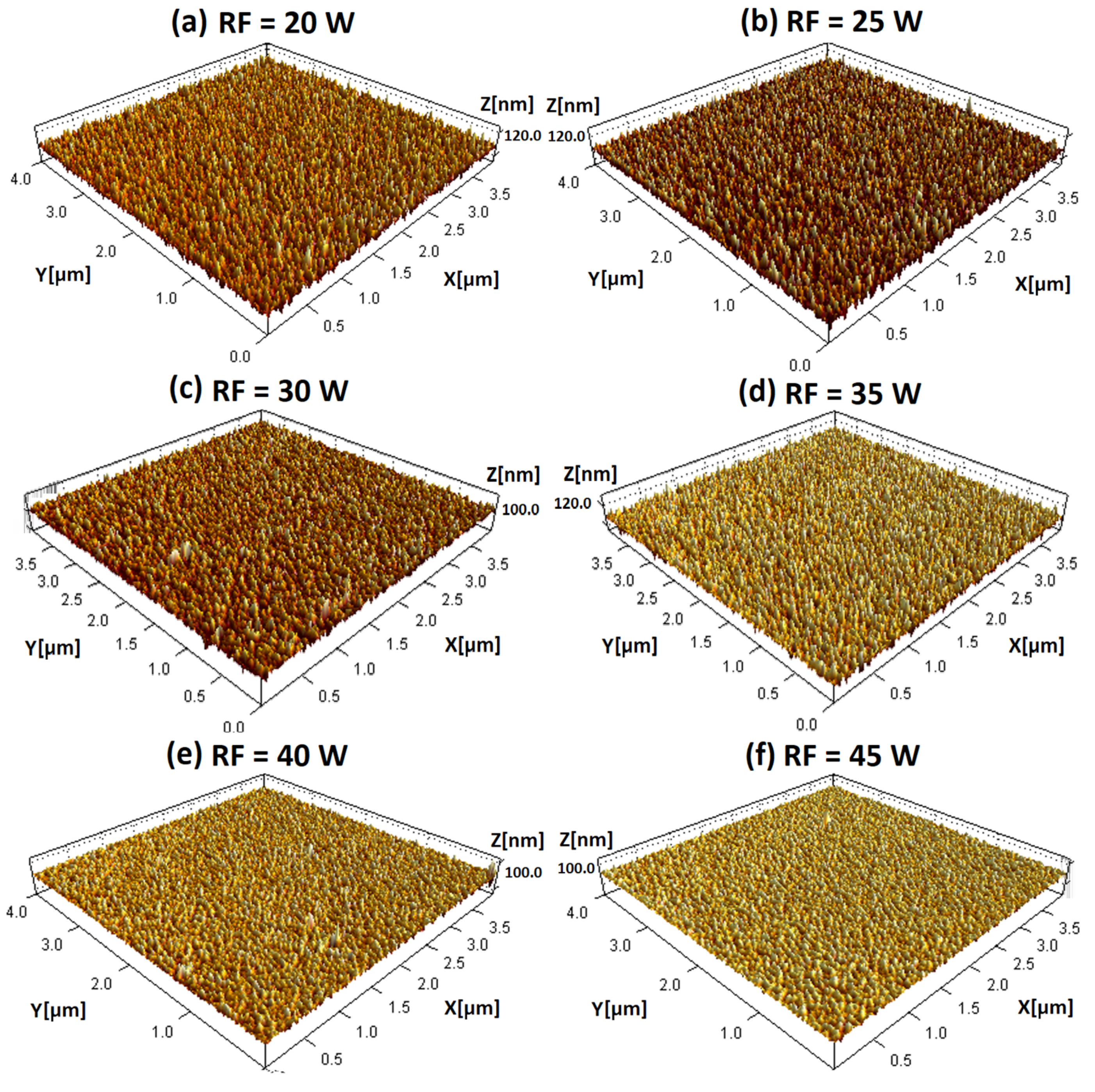
3.1.2. Atomic Force Microscopy

The AFM characterization was performed on the μc-Si:H films deposited on corning glass 2947 substrates in an area of 4 × 4 μm2. Figure 1 shows 3D images of the μc-Si:H films deposited using different RF powers. From these measurements, we extracted the average roughness (Sa) and the root-mean-square (RMS) roughness values, which are included in Table 2.
We employed the Scanning Probe Image Processor (SPIP) software as described in [18] to calculate the average roughness (Sa), which is defined by Equation (1):
S a = 1 M N k = 0 M 1 l = 0 N 1 z x k , y l μ
where M is the data number in the X point, N is the data number in the Y point of the rectangular image, and µ is the mean height defined by Equation (2):
μ = 1 M N K = 0 M 1 l = 0 N 1 z x k , y i
It is clear that there was an increase in film roughness upon increasing the RF power to deposit the films. It has been reported that larger roughness values in μc-Si:H films are associated with large crystal sizes [11]. However, in our characterization, we did not observe a relationship between surface roughness and the XC. A possible explanation is that, with Raman spectroscopy, we are able to calculate the crystalline fraction (Xc), but we do not gain information on crystal sizes. For determining the sizes of crystals, other techniques can be used, such as X-ray diffraction and the Scherrer equation [19,20].

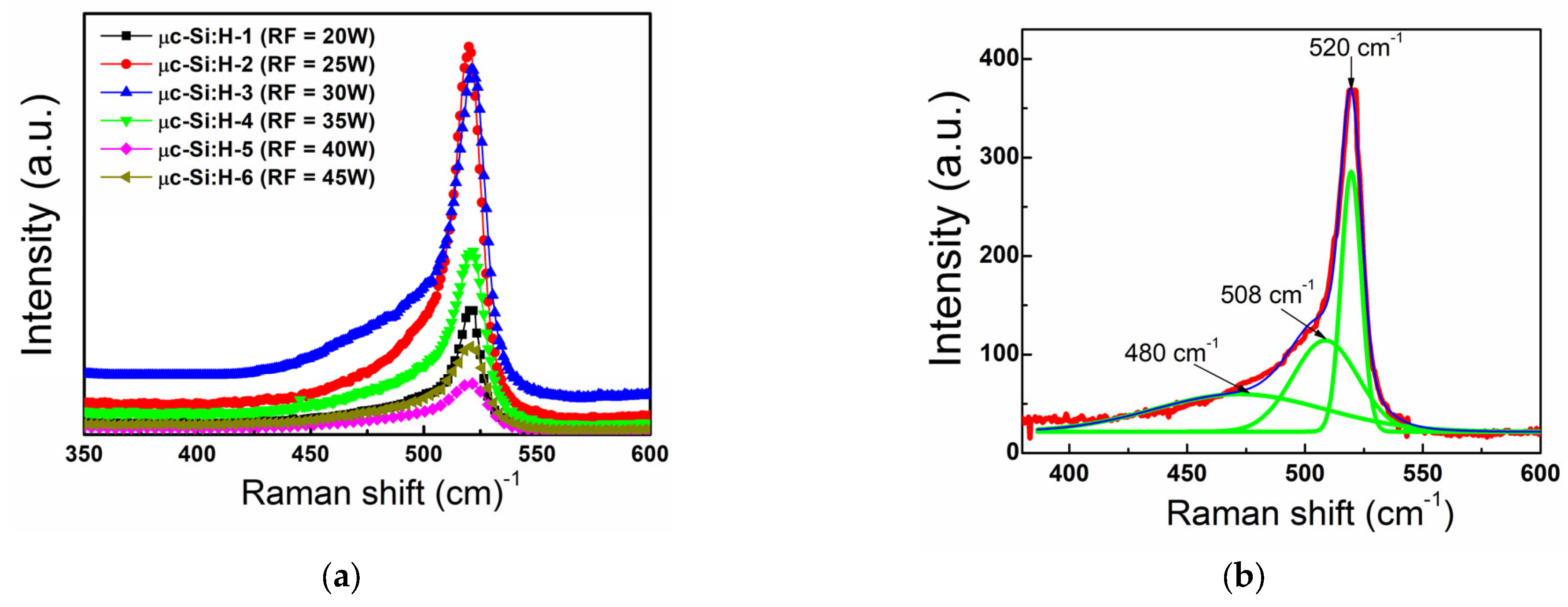
3.1.3. Raman Spectroscopy

As mentioned previously, Raman spectroscopy was used for the μc-Si:H films’ characterization; Figure 2a shows the Raman spectra of the films deposited with different RF power levels, where we can observe a pronounced peak at 520 cm−1 in the spectra. The XC of the films was calculated using the following equation:
XC = (IC + IB)/(IC + IB + IA)
where IC, IB, and IA are the integrated intensities of peaks associated with the crystalline phase at 520 cm−1, an intermediate phase (correlated with small crystal sizes) at 500–514 cm−1, and the amorphous phase at 480 cm−1, respectively [21]. Figure 2b shows the spectrum of a μc-Si:H film with deconvolution in three Gaussian peaks located at 520 cm−1, 508 cm−1, and 480 cm−1. We determined the XC of the μc-Si:H films using Equation (3). Table 2 contains the XC (%) values calculated, where we observed that the XC was in a range of 64–75%, and the film deposited with an RF of 25 W (86.5 mW/cm2) had the largest XC.
As mentioned in Section 2, for the deposition of μc-Si:H, three conditions are required, which are the high dilution of SiH4 in H2, higher chamber pressure, and higher RF power levels than those used for the deposition of a-Si:H. During the deposition of the μc-Si:H films, a H2 etching process can occur [22,23]. From our results, we can see that the etching process is sensitive to the RF power; on the one hand, low RF power produces μc-Si:H with a low XC, while on the other hand, high RF power can promote the H2 etching process, also affecting the XC.

3.1.4. Field Emission Scanning Electron Microscopy

We selected the film with the largest XC (μc-Si:H-2) for scanning electron microscopy analysis (FE-SEM). Figure 3a shows the surface of the μc-Si:H film obtained using FE-SEM with a magnification of 50,000× and an accelerating voltage of 3 kV for the electron beam; we can see that the film surface is composed of grains. Figure 3b shows an amplified image with a magnification of 200,000× and an accelerating voltage of 3 kV, and we can see that the silicon grains are approximately 30–80 nm.
One important aspect is that the film was not prepared for observation; it was analyzed as it was deposited. The quality of the image is an indication that the film is electrically conductive, and this is of importance for the development of TFTs. In Section 3.3, the electrical characterization of the films is reported.

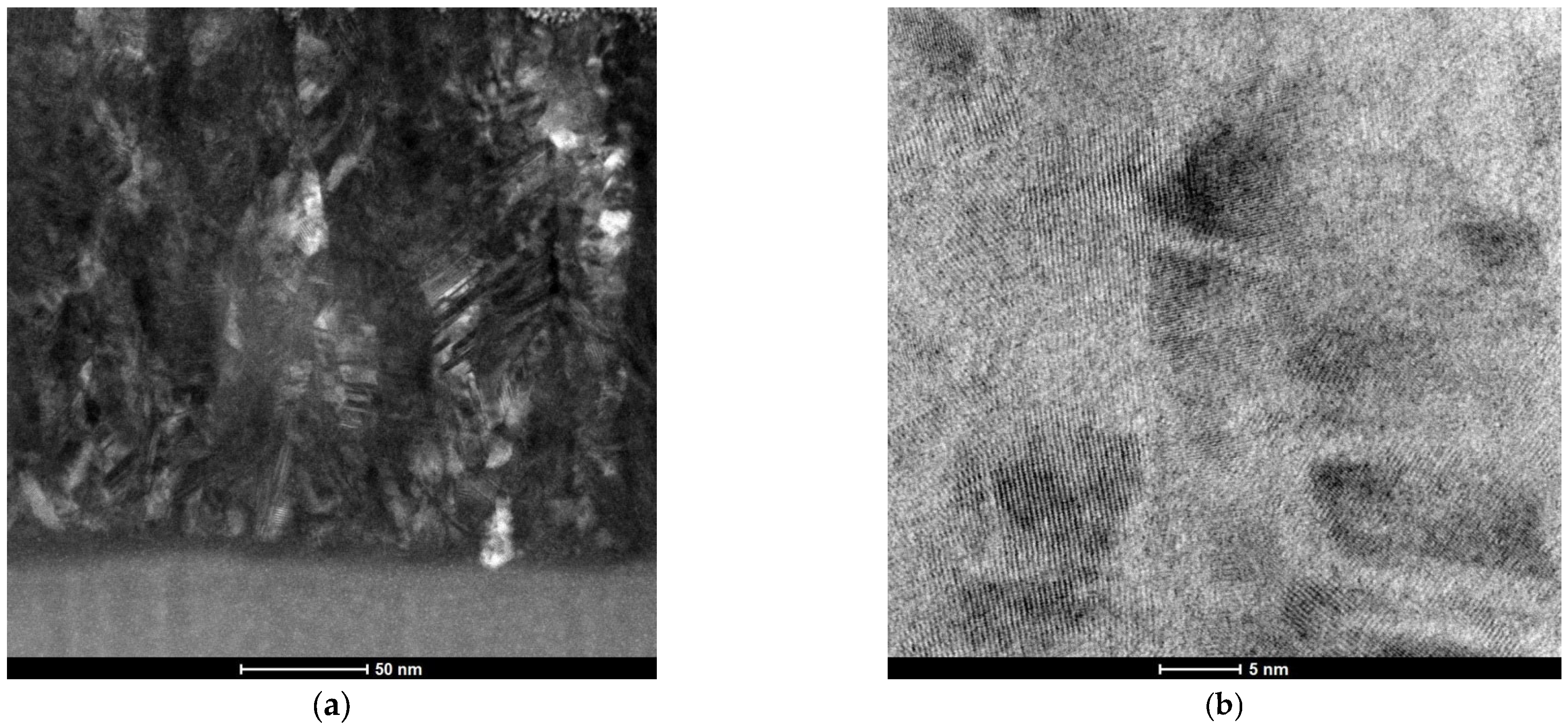
3.1.5. Transmission Electron Microscopy

Even though grains can be observed on the surface of the μc-Si:H film shown in Figure 3, the bulk of the microcrystalline semiconductors was composed of crystalline columns [11,24]. Therefore, in order to analyze the transversal structure of the μc-Si:H film, we used TEM characterization, as described in the previous section. Figure 4a shows a dark-field transversal view of the film (μc-Si:H-2) in an area of 250 × 250 nm2, obtained with an accelerating voltage of 200 keV. In the image, it can be seen that the film effectively grows in crystalline columns, and these columns are of different orientations. Figure 4b shows an amplified transversal view of an area of 50 × 50 nm2, obtained with an accelerating voltage of 200 keV. In this image, we can see, with more detail, different orientations of silicon atoms, and moreover, practically all the area is microcrystalline.

3.2. Optical Characterization

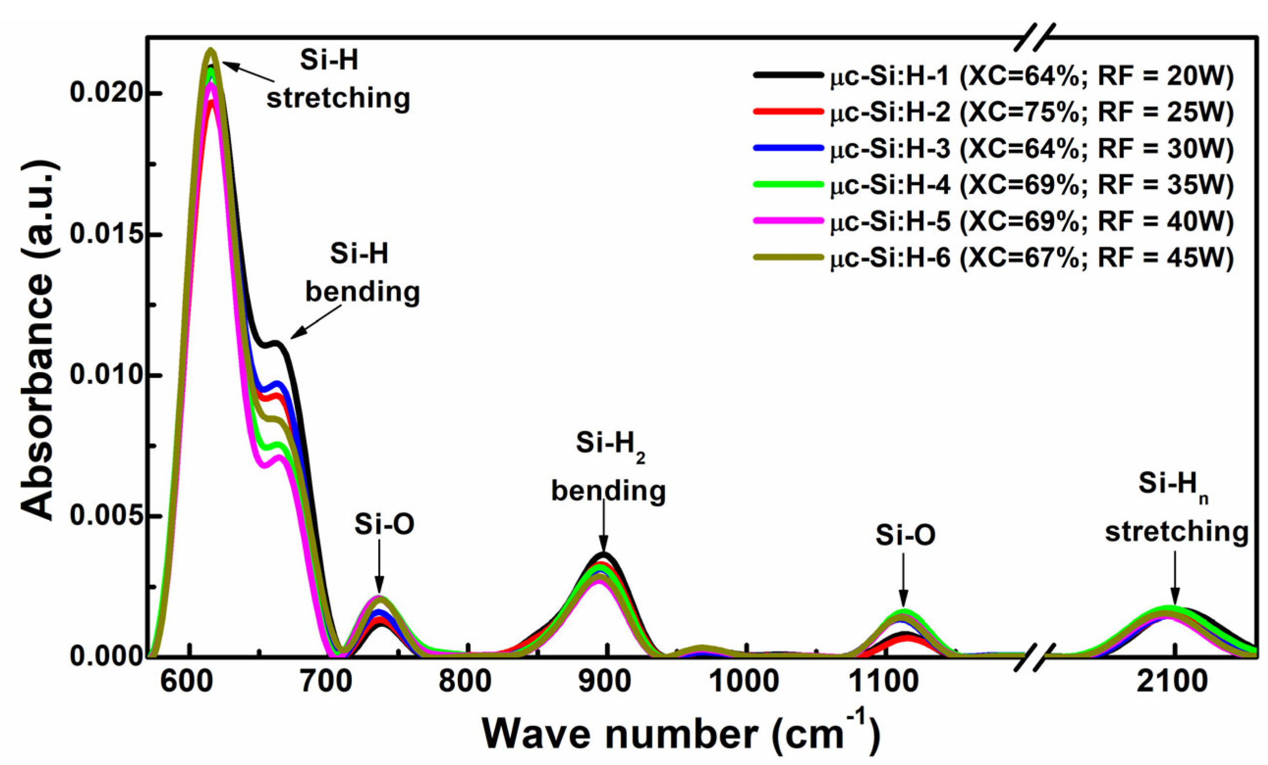
3.2.1. Fourier Transform Infrared Spectroscopy

FTIR spectroscopy was used to characterize the films, as described in Section 2. Figure 5 shows the absorbance spectra of the μc-Si:H film series in a range of 570–2150 cm−1, where several bands are observed, corresponding to different vibration modes.
We observed a band located close to 640 cm−1, which is associated with SiH bonds in bending mode [25]. At approximately 890 cm−1 is a band associated with SiH2 bonds in bending mode [26]. Moreover, two bands associated with Si-O bonds at 750 cm−1 and 1100 cm−1 are observed [26]. Finally, the band at 2000–2200 cm−1 is attributed to SiH, SiH2, and SiH3 stretching modes [27].
The total H2-bonded content (CH) of the films was calculated by integrating the area under the Si-H peak at 640 cm−1 and using Equation (4) [28]:
CH (%) = Aω/NSi ∫ α(ω)/ω dω
where ∫ α(ω)/ω dω is the area of the deconvolution of the peak at 640 cm−1; α is the absorption coefficient at frequency (ω); Aω is the oscillator strength in wagging mode at 640 cm−1 (A(640) = 1.6 × 1019 cm−2) [28]; and NSi = 5 × 1022 cm−3, the atomic density of pure silicon. Table 3 includes the calculated H2-bonded content for the μc-Si:H films, which are in a range of 7.0 to 13.1%.

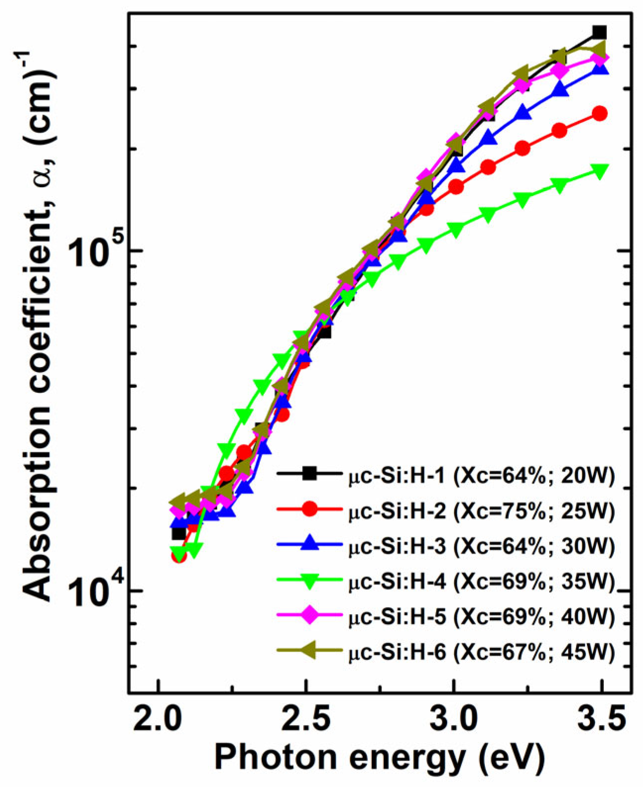
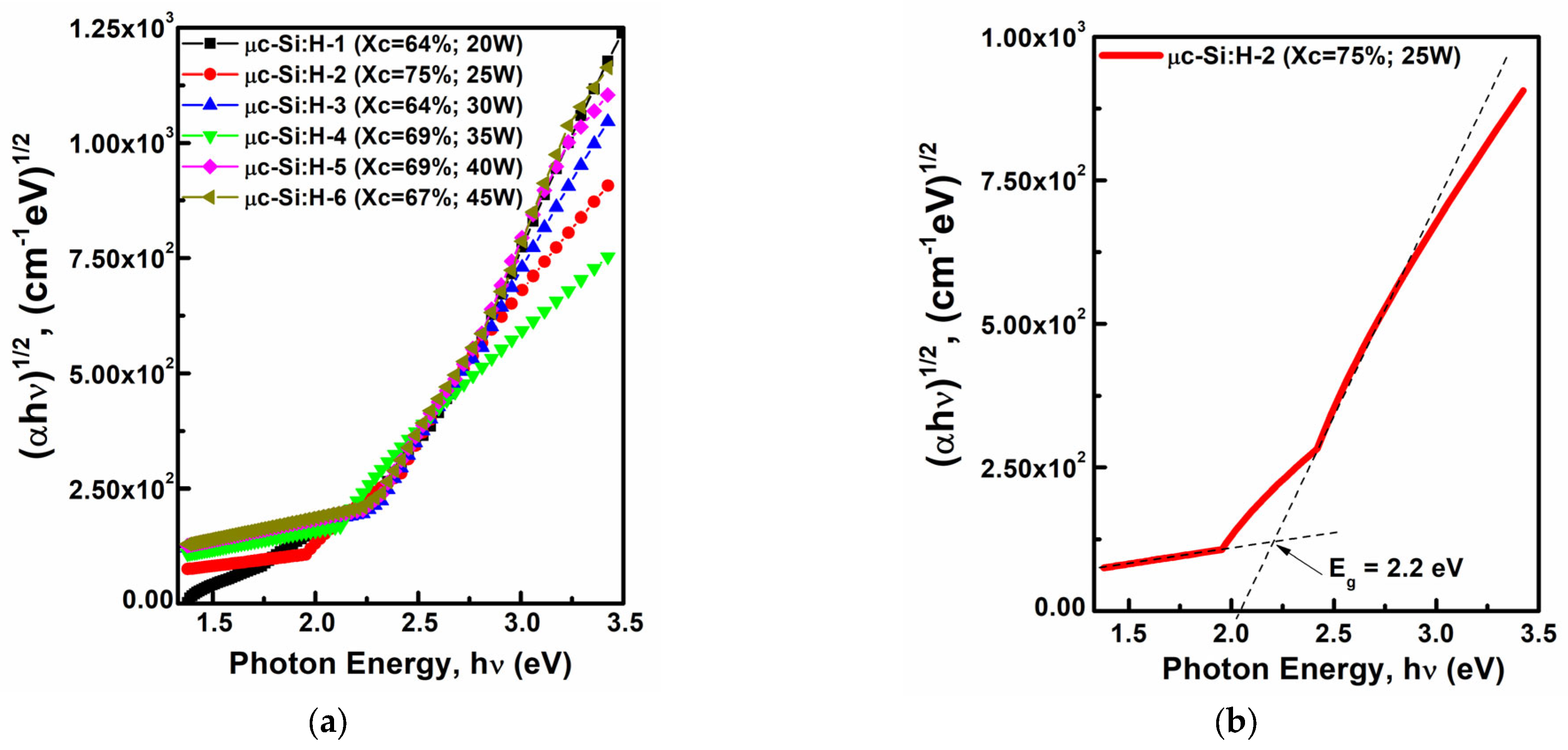
3.2.2. Absorption Coefficient and Determination of the Bandgap

The absorption (α) spectra of the μc-Si:H films deposited on corning glass 1737 substrates were calculated via transmittance measurements using a spectrometer (Perkin-Elmer, Lambda Series) in a wavelength range of 400–900 nm and the Pointwise Unconstrained Minimization Approach [29,30]. Figure 6 shows the α spectra of the μc-Si:H film series in a range of 2 to 3.5 eV. The films with lower Xcs have more absorption in the UV region of the spectra (2.5–3.5 eV), which is in agreement with our previous work, where higher α in the UV region was observed in films with a lower fraction of large crystalline grains [31].
The above is related to the fact that a-Si:H has a larger absorption coefficient in the UV region of the electromagnetic spectrum than µc-Si:H. On the other hand, µc-Si:H has a larger absorption coefficient in the infrared region than a-Si:H [13,14]; these properties are related to their structural arrangements. The µc-Si:H films with lower XCs have a larger amorphous fraction, and therefore, they have larger absorption in the UV region.
The bandgap (Eg) can be calculated using the Tauc plot method. Figure 7a shows the Tauc plots of the different μc-Si:H thin films; α is related to the Eg of the material via the expression of Tauc, that is, Equation (5):
(αhυ)1/2 = B(Eg)
where h is Planck’s constant, v is the frequency of the photon, and B is a constant. From the plot, (αhv)1/2 vs. (hv); the extrapolation of (αhv)1/2 to α =0 (when α > 103 cm−1) provides the Eg. This procedure is accurate for direct bandgap materials such as a-Si:H, but for indirect bandgap materials, such as μc-Si:H, it could provide erroneous results. To obtain more accurate results, we followed the process reported in [17], where a baseline in the sub-bandgap region of the Tauc plot was used, as shown in Figure 7b for the film marked as μc-Si:H-2. The extrapolation of the curve with the baseline provides the Eg value. The Eg values are in a range of 2.1 to 2.48 eV and are shown in Table 2.

3.3. Electrical Characterization

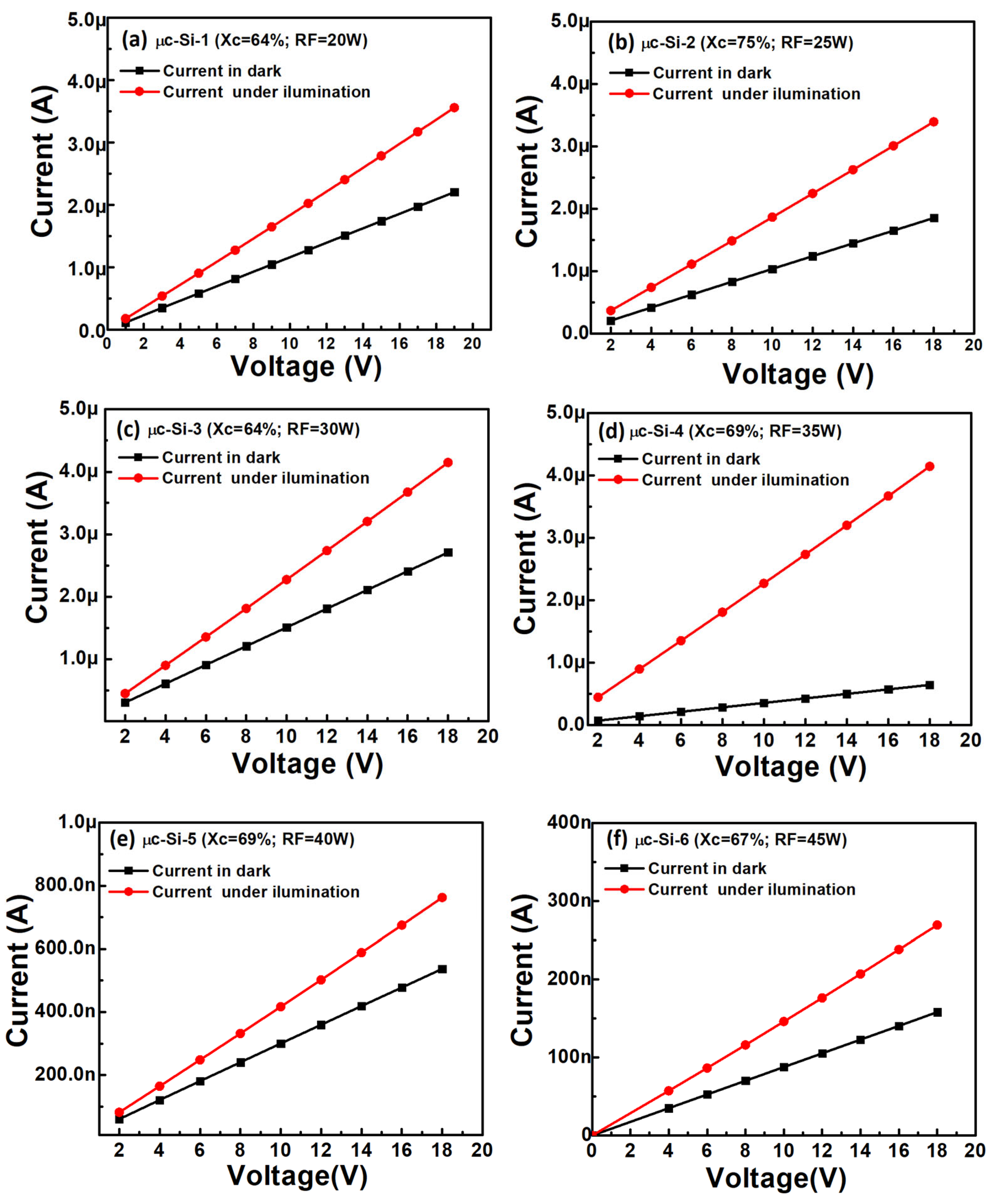
3.3.1. Room Temperature Conductivity and Photoconductivity

To determine the room temperature conductivity (σRT) and photoconductivity (σph) of the films, current–voltage (I-V) measurements were performed in the dark and under illumination, respectively, on the samples deposited on corning glass 2947 with aluminum contacts. Measurements under light were made using the ORIEL SOL 2 solar simulator, which provides light with a standard AM 1.5 spectrum and a power density of 100 mW/cm2. In both measurements, an electrometer (Keithley6517A) was used, configured as a voltage source and current meter.
Figure 8a–f show the current–voltage (I–V) characteristics of the films in the dark and under AM 1.5 radiation, applying a voltage ranging from 0 to 18 V. With the current values and the geometrical parameters of the films, the σRT and σph were calculated. Table 3 shows the σRT and σph values and the photo-response (σphRT) of the deposited µc-Si:H films. The film marked as μc-Si:H-3 has the largest σRT value, while the film labeled as μc-Si:H-4 has the largest σphRT value.
A μc-Si:H film is structurally composed of a crystalline fraction, an amorphous fraction, and voids [31,32]. If the film has a large XC, its σRT value is large as well; on the other hand, if the film has a low XC (and a large amorphous fraction), its σRT value is lower. However, we did not see a correlation between the XC and the σRT. A possible reason is the undesirable oxygen doping of the films during deposition, which can increase the σRT. In fact, the film with the lowest EA (as shown below) had the largest σRT, which makes sense since doping reduces the EA.
Furthermore, oxygen doping can be the reason for larger σRT values in these μc-Si:H films than those reported in the literature [33]. Moreover, in µc-Si:H, the σph is affected by the XC of the film and the SiH4 concentration during deposition. It has been reported that in μc-Si:H intrinsic films with large XCs the change from σRT to σph is lower than one order of magnitude [33].

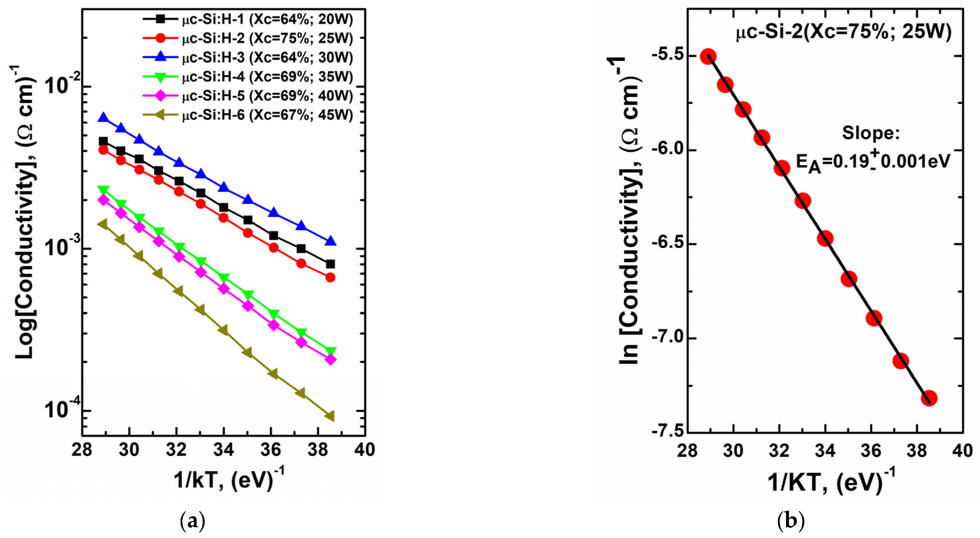
3.3.2. Temperature Dependence of Conductivity and Activation Energy

Temperature dependence of conductivity (σ(T)) measurements were performed on the films deposited on corning glass 2947 with aluminum contacts. The samples were collocated inside a cryostat at a pressure of 60 mTorr. Voltage was applied in a range of −20 to 20 V on the samples, and the current was measured using an electrometer (Keithley6517A) in a range of temperature of 27 to 127 °C. Finally, the dark conductivity (σD) was calculated using the films’ geometrical parameters. Figure 9a shows the Log(σD) vs. 1/kT, where k is the Boltzmann constant, and T is the temperature.
The σD, T, and EA are related by an Arrhenius-type Equation (6):
σD = σ0 exp [−EA/kT]
where k is the Boltzmann constant, and σ0 is a pre-exponential factor; the previous equation can be expressed as Equation (7):
Ln (σD) = Ln (σ0) − EA/kT
Equation (7) has the form of the equation depicting a straight line (y = A+ Bx). Experimentally, the activation energy is obtained from the slope of the graph of ln (σD) vs. 1/kT, as shown in Figure 9b, corresponding to the film labeled as μc-Si:H-2. A linear fit of the experimental data points was performed, and the slope was extracted.
Table 3 shows the EA values of the μc-Si:H film series, where we can see that the EA values are low, indicating that the films were unintentionally doped, possibly with oxygen, which was incorporated into the film during deposition. This result agrees with the FTIR characterization, where pronounced peaks can be observed in the 1000–1200 cm−1 region, which is related to Si-O bonds. Moreover, as the dopant is oxygen, the µc-Si:H films are n-type.

4. Discussion

From the previous analysis of the μc-Si:H film series, we saw that, effectively, there is an optimal RF power level that can obtain a large XC in films deposited by PECVD. An RF power of 25 W (86.5 mW/cm2), coupled with a large H2/SiH4 ratio, resulted in an XC of 75%. Larger or lower RF power levels resulted in films with lower XCs.
From the FE-SEM characterization, we observed that the film surface seems to be composed of grains of sizes ranging from 30 to 80 nm; however, from the TEM analysis, we observed that the films grew in columns (Figure 4a) with a thin initial incubation layer, which is of an amorphous nature. A larger magnification in the analysis of the columns (Figure 4b) gave us information on the microcrystalline nature of the film, and several crystalline orientations are observed.
From the optical characterization, we observed that the total H2 content (CH) of the μc-Si:H films was in a range of 7.0–13.1%, which agrees with the results reported in [28,34]. Furthermore, we observed that the Eg values of the μc-Si:H film series were in a range of 2.1–2.48 eV; these values are larger than those reported in [35] and are also larger than those values of a-Si:H, which are in a range of 1.6–1.88 eV [36]. The film with the largest XC had an Eg of 2.2 eV, and we did not observe any trend related to the deposition RF power.
The electrical characterization gave us information on several parameters of the μc-Si:H films. The σRT was in a range of 8.3 × 10⁻⁵–1.2 × 10⁻³ (Ωcm)−1, while the film with the largest XC had a σRT of 6.4 × 10⁻⁴ (Ωcm)−1. This value is larger than those reported in the literature [24], and it is possibly related to unintentional doping with O2 during the deposition of the films. The above is corroborated by a peak at 1000–1200 cm−1 in the films’ absorbance spectra obtained via FTIR spectroscopy, which was related to Si-O bonds. Furthermore, the small EA values were in a range of 0.18 to 0.28 eV, indicating that the films are not intrinsic.
On the other hand, the σph values were in a range of 1.4 × 10⁻⁴–1.8 × 10⁻³ (Ωcm)−1, and the σphRT ratio was in a range of 1.5–6.4. The film with the lowest XC had the largest σphRT ratio (of 6.4), which agrees with the fact that the more amorphous a film is, the more photoconductive it is.
It is important to produce μc-Si:H films with large XC values since this is related to both larger µe and larger absorption in the infrared region of the electromagnetic spectrum [13,14,15,16]. These properties are important for the development of faster TFTs and tandem (a-Si:H/μc-Si:H) solar cells with high conversion efficiency, respectively. Moreover, it is important to control the deposition RF power since large values produce excessive powder in the deposition chamber and can damage the vacuum pumps of the PECVD deposition system. In this work, we demonstrated that a high RF power is not necessary to obtain μc-Si:H films with a large XC, and consequently, the powder formed in the deposition chamber was reduced significantly, preserving the integrity of the vacuum pumps.

5. Conclusions

In this work, we studied μc-Si:H films deposited using the PECVD technique at 200 °C with a SiH4, H2, and Ar mixture. Particularly, we focused our study on the effect of the deposition RF power and the XC of μc-Si:H films, and these were correlated with their structural, optical, and electrical properties. We found an optimal RF power value of 25 W (an RF power density of 86.5 mW/cm2) for producing films with high XC values (75%), coupled with a high H2/SiH4 ratio (of 50) and a high chamber pressure (of 1500 mTorr). Even though the films were deposited without any unintentional doping, they were highly conductive, and furthermore, they had low EA values, indicating their non-intrinsic nature. Using electron microscopy, we observed that, effectively, the films grew in crystalline columns, and these columns were of different orientations. We can stress that producing μc-Si:H films with high XCs will result in high-performance devices, such as TFTs and a-Si:H/μc-Si:H tandem solar cells, where high µe and high absorption in the infrared spectrum are necessary, respectively. Finally, we produced μc-Si:H films with large XC values using relatively low RF power densities, significantly reducing powder formation in the plasma and preserving the integrity of the vacuum pumps of the PECVD system.

Author Contributions

Conceptualization, M.M., P.R., A.T.-S. and A.T.; methodology, A.M., A.T.-S., A.T., J.F., L.H. and C.Z.; validation, P.R., A.T.-S. and C.A.; formal analysis, M.M., A.M., A.T., P.R. and A.A.; investigation M.M., A.M., L.H. and C.A.; writing—original draft preparation, M.M., J.F. and C.Z.; writing—review and editing, J.F., L.H., C.Z. and A.A.; visualization, M.M., P.R., A.T. and A.T.-S.; supervision, M.M., C.A. and A.A. All authors have read and agreed to the published version of the manuscript.

Funding

This research received no external funding.

Data Availability Statement

Not applicable.

Acknowledgments

This work was supported by the National Council of Humanities, Sciences and Technologies of Mexico (CONAHCYT).

Conflicts of Interest

The authors declare no conflict of interest.

References

  1. Spear, W.E.; Le Comber, P.G.; Kinmond, S.; Brodsky, M.H. Amorphous silicon p-n junction. Appl. Phys. Lett. 1976, 28, 105–107. [Google Scholar] [CrossRef]
  2. Schropp, R.E.I.; Zeman, M. New Developments in Amorphous Thin-Film Silicon Solar Cells. IEEE Trans. Electron Dev. 1999, 46, 2086–2092. [Google Scholar] [CrossRef]
  3. Ichikawa, Y.; Yoshida, T.; Hama, T.; Sakai, H.; Harashima, K. Production technology for amorphous silicon-based flexible solar cells. Sol. Energy Mater. Sol. Cells 2001, 66, 107–115. [Google Scholar] [CrossRef]
  4. Sonntag, P.; Preissler, N.; Bokalič, M.; Trahms, M.; Haschke, J.; Schlatmann, R.; Topič, M.; Rech, B.; Amkreutz, D. Silicon Solar Cells on Glass with Power Conversion Efficiency above 13% at Thickness below 15 Micrometer. Sci. Rep. 2017, 7, 873. [Google Scholar] [CrossRef] [PubMed] [Green Version]
  5. Powell Martin, J. The physics of amorphous-silicon thin-film transistors. IEEE Trans. Electron Dev. 1989, 36, 2753–2763. [Google Scholar] [CrossRef]
  6. Flewitt, A.J. Hydrogenated Amorphous Silicon Thin-Film Transistors (a-Si:H TFTs). In Handbook of Visual Display Technology; Blankenbach, K., Yan, Q., O’Brien, R.J., Eds.; Springer: Berlin/Heidelberg, Germany, 2014; pp. 1–18. [Google Scholar]
  7. Tanaka, K.; Matsuda, A. Glow-discharge amorphous silicon: Growth process and structure. Mater. Sci. Rep. 1987, 2, 139–184. [Google Scholar] [CrossRef]
  8. Staebler, D.L.; Wronski, C.R. Reversible conductivity changes in discharge-produced amorphous Si. Appl. Phys. Lett. 1977, 31, 292–294. [Google Scholar] [CrossRef]
  9. Bronner, W.; Kleider, J.P.; Bruggemann, R.; Mencaraglia, D.; Mehring, M. Comparison of transport and defects properties in hydrogenated polymorphous and amorphous silicon. J. Non-Cryst. Solids 2002, 299–302, 551–555. [Google Scholar] [CrossRef]
  10. Joubert, P.; Loisel, B.; Chouan, Y.; Haji, L. The Effect of Low Pressure on the Structure of LPCVD Polycrystalline Silicon Films. J. Electrochem. Soc. 1987, 134, 2541–2545. [Google Scholar] [CrossRef]
  11. Shah, A.; Vallat-Sauvain, E.; Torres, P.; Meier, J.; Kroll, U.; Hof, C.; Droz, C.; Goerlitzer, M.; Wyrsch, N.; Vanecek, M. Intrinsic microcrystalline silicon (μc-Si:H) deposited by VHF-GD (very high frequency-glow discharge): A new material for photovoltaics and optoelectronics. Mater. Sci. Eng. B 2000, 69–70, 219–226. [Google Scholar] [CrossRef]
  12. Dorostghol, Z.; Kosarian, A. Improving structural, optical, and electrical properties of μc-Si:H using non-uniform hydrogen dilution treatment on RF-PECVD prepared layers. Mat. Sci. Semicon. Proc. 2021, 129, 105790. [Google Scholar] [CrossRef]
  13. Fischer, D.; Dubail, S.; Selvan, J.A.A.; Vaucher, N.P.; Platz, R.; Hof, C.H.; Kroll, U.; Meier, J.; Torres, P.; Keppner, H.; et al. The “micromorph” solar cell: Extending a-Si:H technology towards thin film crystalline silicon. In Proceedings of the Conference Record of the Twenty Fifth IEEE Photovoltaic Specialists Conference, Washington, DC, USA, 6 August 1996. [Google Scholar]
  14. Keppner, H.; Meier, J.; Torres, P.; Fischer, D.; Shah, A. Microcrystalline silicon and micromorph tandem solar cells. Appl. Phys. A 1999, 69, 169–177. [Google Scholar] [CrossRef] [Green Version]
  15. Chan, K.-Y.; Knipp, D.; Gordijn, A.; Stiebig, H. Influence of crystalline volume fraction on the performance of high mobility microcrystalline silicon thin-film transistors. J. Non-Cryst. Solids 2008, 354, 2505–2508. [Google Scholar] [CrossRef]
  16. Cabarrocas, P.R.I.; Morral, A.F.I.; Lebib, S.; Poissant, Y. Plasma production of nanocrystalline silicon particles and polymorphous silicon thin films for large-area electronic devices. Pure Appl. Chem. 2002, 74, 359–367. [Google Scholar] [CrossRef]
  17. Makuła, P.; Pacia, M.; Macyk, W. How To Correctly Determine the Band Gap Energy of Modified Semiconductor Photocatalysts Based on UV–Vis Spectra. J. Phys. Chem. Lett. 2018, 9, 6814–6817. [Google Scholar] [CrossRef] [Green Version]
  18. Luna-López, J.A.; Morales-Sánchez, A.; Aceves-Mijares, M.; Yu, Z.; Domínguez, C. Analysis of surface roughness and its relationship with photoluminescence properties of silicon-rich oxide films. J. Vac. Sci. Technol. A 2009, 27, 57–62. [Google Scholar] [CrossRef]
  19. Langford, J.I.; Wilson, A.J.C. Scherrer after Sixty Years: A Survey and Some New Results in the Determination of Crystallite Size. J. Appl. Cryst. 1978, 11, 102–113. [Google Scholar] [CrossRef]
  20. Veprek, S.; Sarott, F.-A.; Rückschloss, M. Temperature dependence of the crystallite size and crystalline fraction of microcrystalline silicon deposited from silane by plasma CVD. J. Non-Cryst. Solids 1991, 137–138, 733–736. [Google Scholar] [CrossRef]
  21. Viera, G.; Huet, S.; Boufendi, L. Crystal size and temperature measurements in nanostructured silicon using Raman spectroscopy. J. Appl. Phys. 2001, 90, 4175–4183. [Google Scholar] [CrossRef]
  22. Drevillon, B.; Solomon, I.; Fang, M. The Physics of Plasma Deposition of Microcrystalline Silicon. Mat. Res. Soc. Symp. Proc. 1993, 283, 455–462. [Google Scholar] [CrossRef]
  23. Solomon, I.; Drévillon, B.; Shirai, H.; Layadi, N. Plasma deposition of microcrystalline silicon: The selective etching model. J. Non-Cryst. Solids 1993, 164–166, 989–992. [Google Scholar] [CrossRef]
  24. Vetterl, O.; Finger, F.; Carius, R.; Hapke, P.; Houben, L.; Kluth, O.; Lambertz, A.; MuKck, A.; Rech, B.; Wagner, H. Intrinsic microcrystalline silicon: A new material for photovoltaics. Sol. Energy Mater. Sol. Cells 2000, 62, 97–108. [Google Scholar] [CrossRef]
  25. Goldie, D.M.; Persheyev, S.K. Quantitative hydrogen measurements in PECVD and HWCVD a-Si:H using FTIR spectroscopy. J. Mater. Sci. 2006, 41, 5287–5291. [Google Scholar] [CrossRef]
  26. Han, D.; Wang, K.; Owens, J.M.; Gedvilas, L.; Nelson, B.; Habuchi, H.; Tanaka, M. Hydrogen structures and the optoelectronic properties in transition films from amorphous to microcrystalline silicon prepared by hot-wire chemical vapor deposition. J. Appl. Phys. 2003, 93, 3776–3783. [Google Scholar] [CrossRef]
  27. Tang, Z.; Wang, W.; Zhou, B.; Wang, D.; Peng, S.; He, D. The influence of H2/(H2 + Ar) ratio on microstructure and optoelectronic properties of microcrystalline silicon films deposited by plasma-enhanced CVD. Appl. Surf. Sci. 2009, 255, 8867–8873. [Google Scholar] [CrossRef]
  28. Kroll, U.; Meier, J.; Shah, A. Hydrogen in amorphous and microcrystalline silicon films prepared by hydrogen dilution. J. Appl. Phys. 1996, 80, 4971–4975. [Google Scholar] [CrossRef]
  29. Birgin, E.G.; Chambouleyron, I.; Martínez, J.M. Estimation of optical constants of thin films using unconstrained optimization. J. Comput. Phys. 1999, 151, 862–880. [Google Scholar] [CrossRef] [Green Version]
  30. Mulato, M.; Chambouleyron, I.; Birgin, E.G.; Martínez, J.M. Determination of thickness and optical constants of a-Si:H films from transmittance data. Appl. Phys. Lett. 2000, 77, 2133–2135. [Google Scholar] [CrossRef] [Green Version]
  31. Moreno, M.; Boubekri, R.; Cabarrocas, P.R.I. Study of the effects of different fractions of large grains of µc-Si:H:F films on the infrared absorption on thin film solar cells. Sol. Energy Mater. Sol. Cells 2012, 100, 16–20. [Google Scholar] [CrossRef]
  32. Moreno, M.; Ponce, A.; Galindo, A.; Ortega, E.; Morales, A.; Flores, J.; Ambrosio, R.; Torres, A.; Hernandez, L.; Vazquez-Leal, H.; et al. Comparative Study on the Quality of Microcrystalline and Epitaxial Silicon Films Produced by PECVD Using Identical SiF4 Based Process Conditions. Materials 2021, 14, 6947. [Google Scholar] [CrossRef]
  33. Astakhov, O. Relationship between defect density and charge carrier transport in amorphous and microcrystalline silicon. Phys. Rev. B 2009, 79, 104205. [Google Scholar] [CrossRef] [Green Version]
  34. Remes, Z.; Vanecek, M.; Torres, P.; Kroll, U.; Mahan, A.H.; Crandall, R.S. Optical determination of the mass density of amorphous and microcrystalline silicon layers with different hydrogen contents. J. Non-Cryst. Solids 1998, 227–230, 876–879. [Google Scholar] [CrossRef] [Green Version]
  35. Wei, L.; Donglin, X.; Huifang, W.; Xiujian, Z. Hydrogenated nanocrystalline silicon thin film prepared by RF-PECVD at high pressure. J. Non-Cryst. Solids 2010, 356, 2552–2556. [Google Scholar]
  36. Hishikawa, Y.; Nakamura, N.; Tsuda, S.; Nakano, S.; Kishi, Y.; Kuwano, Y. Interference-Free Determination of the Optical Absorption Coefficient and the Optical Gap of Amorphous Silicon Thin Films. Jap. J. Appl. Phys. 1991, 30, 1008–1014. [Google Scholar] [CrossRef]
Figure 1. AFM images of the series of μc-Si:H films deposited with different RF power levels: (a) RF = 20 W, (b) RF = 25 W, (c) RF = 30 W, (d) RF = 35 W, (e) RF = 40 W, and (f) RF = 45 W.
Electronicmat 04 00009 g001
Figure 2. (a) Raman spectra of the series of μc-Si:H films deposited with different RF power levels; (b) Raman spectra of the film deposited with an RF power of 25 W (86.5 mW/cm2), where the deconvolution of the spectrum in three Gaussian peaks at 520 cm−1, 508 cm−1, and 480 cm−1 is shown.
Electronicmat 04 00009 g002
Figure 3. Field emission scanning electron microscopy (FE-SEM) analysis of the surface of the μc-Si:H film deposited with an RF power of 25 W (86.5 mW/cm2): (a) magnification at 50,000×; (b) magnification at 200,000×.
Electronicmat 04 00009 g003
Figure 4. Transmission electron microscopy (TEM) analysis of the surface of the μc-Si:H film deposited with an RF power of 25 W (86.5 mW/cm2): (a) area observed at 250 × 250 nm2; (b) area observed at 50 × 50 nm2.
Electronicmat 04 00009 g004
Figure 5. FTIR absorbance spectra of the series of μc-Si:H films deposited at different RF power levels.
Electronicmat 04 00009 g005
Figure 6. Absorption coefficient of the series of μc-Si:H films deposited at different RF power levels.
Electronicmat 04 00009 g006
Figure 7. (a) Tauc plots of the series of μc-Si:H films deposited with different RF powers; (b) extraction of Eg for the film marked as μc-Si:H-2.
Electronicmat 04 00009 g007
Figure 8. I–V characteristics of the μc-Si:H films deposited at different RF power levels in the dark and under AM 1.5 radiation: (a) RF = 20 W, (b) RF = 25 W, (c) RF = 30 W, (d) RF = 35 W, (e) RF = 40 W, and (f) RF = 45 W.
Electronicmat 04 00009 g008
Figure 9. (a) Temperature dependence of conductivity (σ(T)) of the series of μc-Si:H films deposited with different RF power levels; (b) extraction of EA for the film marked as μc-Si:H-2, which has a larger XC.
Electronicmat 04 00009 g009
Table 1. Deposition parameters of the series of μc-Si:H films. The deposition time was 30 min, and the temperature was 200 °C.
SamplePressure
(mTorr)
RF
Power
(W)
RF Power
Density
(mW/cm2)
SiH4
10% in H2
(Sccm)
H2
(Sccm)
Ar
(Sccm)
H2/SiH4
Ratio
μc-Si:H-115002069.210411050
μc-Si:H-215002586.510411050
μc-Si:H-3150030103.810411050
μc-Si:H-4150035121.110411050
μc-Si:H-5150040138.410411050
μc-Si:H-6150045155.710411050
Table 2. Properties of the series of μc-Si:H films obtained from structural characterization.
SampleThickness
(nm)
Deposition
Rate
(Å/s)
Average
Roughness
(nm)
RMS
Roughness
(nm)
Crystalline Fraction, XC
(%)
μc-Si:H-11811.091.121.4664
μc-Si:H-21600.881.211.6775
μc-Si:H-31610.891.571.9564
μc-Si:H-41640.911.231.6569
μc-Si:H-51570.871.572.1269
μc-Si:H-61450.801.862.4867
Table 3. Properties of the series of μc-Si:H films obtained using optical and electrical characterization; XC is included to correlate it with the other film parameters.
SampleCrystalline
Fraction, XC (%)
CH
(%)
Eg
(eV)
σRT
(Ωcm)−1
σph
(Ωcm)−1
σphRTEA
(eV)
μc-Si:H-16410.32.466.9 × 10−41.1 × 10−31.60.18
μc-Si:H-2759.42.26.4 × 10−41.0 × 10−31.80.19
μc-Si:H-3649.42.371.2 × 10−31.8 × 10−31.50.17
μc-Si:H-4697.02.102.2 × 10−41.4 × 10−36.40.23
μc-Si:H-5697.22.422.3 × 10−43.3 × 10−41.40.22
μc-Si:H-66713.12.488.3 × 10−51.4 × 10−41.70.28
Disclaimer/Publisher’s Note: The statements, opinions and data contained in all publications are solely those of the individual author(s) and contributor(s) and not of MDPI and/or the editor(s). MDPI and/or the editor(s) disclaim responsibility for any injury to people or property resulting from any ideas, methods, instructions or products referred to in the content.

