Article

Exploring the Impact of Fe-Implantation on the Electrical Characteristics of Al/p-Si Schottky Barrier Diodes

by
Joseph Oluwadamilola Bodunrin
1,*,
Duke Ateyh Oeba
2 and
Sabata Jonas Moloi
1
1
Department of Physics, College of Science, Engineering and Technology, University of South Africa, Private Bag X6, Florida 1710, South Africa
2
Department of Physics, Egerton University, Njoro P.O. Box 536-20115, Kenya
*
Author to whom correspondence should be addressed.
Electron. Mater. 2023, 4(2), 95-109; https://doi.org/10.3390/electronicmat4020008
Submission received: 17 April 2023 / Revised: 8 June 2023 / Accepted: 13 June 2023 / Published: 16 June 2023

Abstract

:
The effects of Fe-implantation on the electrical characteristics of Au/p-Si Schottky barrier diodes (SBDs) were studied using current–voltage (IV) and capacitance–voltage (CV) techniques. The Rutherford Backscattering Spectrometry (RBS) and Energy Dispersive Spectroscopy (EDS) results showed that Fe ions are well implanted and present in the Fe-implanted Si material. The acquired results from IV and CV analysis showed that the diodes were well fabricated, and Fe-implantation changed the normal diode’s IV behaviour from typical exponential to ohmic. The ohmic behaviour was described in terms of the defect levels induced by Fe in the middle of the band gap of Si. The conduction mechanism for both forward and reverse currents was presented, and the effect of Fe-implantation on the conduction mechanisms was investigated. The CV results show that Fe generates a high density of minority carriers in p-Si, which agreed with the increase in reverse current observed in the IV results. The diode parameters in terms of saturation current, ideality factor, Schottky barrier height, doping density, and space charge region (SCR) width were used to investigate the effect of Fe in p-Si based diode. Owing to the observed changes, which were analogous to those induced by dopants that improve the radiation hardness of silicon, it was safe to say that Fe can also assist in the quest to improve the radiation hardness of silicon using the defect-engineering method.

1. Introduction

Schottky barrier diodes (SBDs) are the building blocks of a variety of semiconductor electronic devices, including solar cells, photodetectors, field-effect transistors (FETs), and semiconductor-based detectors. In these diodes, the formed metal-semiconductor (m-s) junctions allow the current to flow in one direction, and their forward current is made up of the majority carriers injected into the junction from the semiconductor. Silicon (Si) is an essential semiconductor that has been used for the fabrication of devices, and its choice can be attributed to its cheap cost, resilience, and well-known technology, amongst other advantages. However, a major challenge associated with Si-based devices used as radiation detectors is that they suffer severe radiation damage, resulting in a degradation in their performance [1,2].
As a result of radiation-induced defects that act as generation and recombination (g-r) centres, the leakage current increases [3,4]. High leakage current has a detrimental impact on detector performance by lowering the signal-to-noise ratio (SNR) and increasing the power consumption [5]. Furthermore, the efficacy of the detector deteriorates because of the free-charge carrier traps produced by radiation-induced defects. In a bid to address these challenges, it is necessary to improve the radiation hardness of Si. An improved radiation hardness of Si will enable the devices to perform efficiently in high radiation environments, such as high energy physics experiments (HEPE).
Studies have shown that doping with dopants such as gold (Au) and platinum (Pt) improves the radiation hardness of Si [6,7,8]. The effects of Au and Pt dopants on the electrical properties of Si-based devices have been studied previously [6,7,8,9,10]. Au induces defect levels at E C − 0.34 eV, E C  − 0.55 eV, and E V + 0.34 eV [6,10] in the band gap of Si, where E C is the bottom of the conduction band and E V is the top of the valence band. Pt, on the other hand, creates defect levels in the Si band gap at E C  − 0.23 eV, E C  − 0.52 eV, and E V + 0.36 eV [7,10]. It is worth noting that Au and Pt induce a common defect level that can be referred to as a “midgap defect”, a defect level located at the middle of the Si band gap. These defect levels are responsible for the relaxation behaviour of Si, thereby improving its radiation hardness [11]. Though these metals have demonstrated the ability to suppress the effects of radiation damage to Si [6,12], they are prohibitively expensive for research. Further, Au and Pt create other defect levels located at E C   − 0.36, E V   + 0.34, and E C  − 0.23 eV, which change the material’s conductivity, thereby reducing the sensitivity of the Si-based detector. These shortcomings have prompted an urgent search for alternative dopants in an effort to enhance the electrical characteristics of Si-based devices for radiation-sensing applications.
Iron (Fe) is a transitional metal that has an electronic configuration of {Ar}3d6 4s2 with two valence electrons. The properties of Fe in Si have been previously investigated [13,14,15]. Fe diffuses interstitially in Si, introducing defect levels in the Si band gap at E C  − 0.55 eV, E V + 0.40, and E C  − 0.27 eV [13]. The defect level at E V + 0.40 increases the concentration of minority carriers in p-Si, hence the conductivity of the material. The Fe-induced defect levels at E C  − 0.27 eV and E C  − 0.55 eV are donor levels and are expected to reduce the charge carrier’s density, resulting in an increase in the resistivity of the device fabricated on Fe-implanted p-Si material. As a result, the effects of Fe-implantation on the conductivity/resistivity of Si are important to fully comprehend the effect of Fe in Si.
The defect level of the main interest caused by Fe in Si is E C  − 0.55 eV, the defect level positioned in the middle of the band gap of Si. The defect level is comparable to those induced by Au and Pt [6,7,8,16] and has been reported to be responsible for the relaxation behaviour of the material [8]. Diodes fabricated on a relaxation material have been reported to have high electrical resistivity as well as ohmic IV behaviour. In addition, these materials are resistant to radiation damage [8,11].
The electrical measurements (IV and CV) were performed on the Schottky diodes fabricated on unimplanted and Fe-implanted p-Si in this study. The purpose of this work was to study the effect of Fe-implantation on the electrical properties/characteristics of Si diodes and to juxtapose the results with those reported on Au- and Pt-doped Si diodes in past studies.

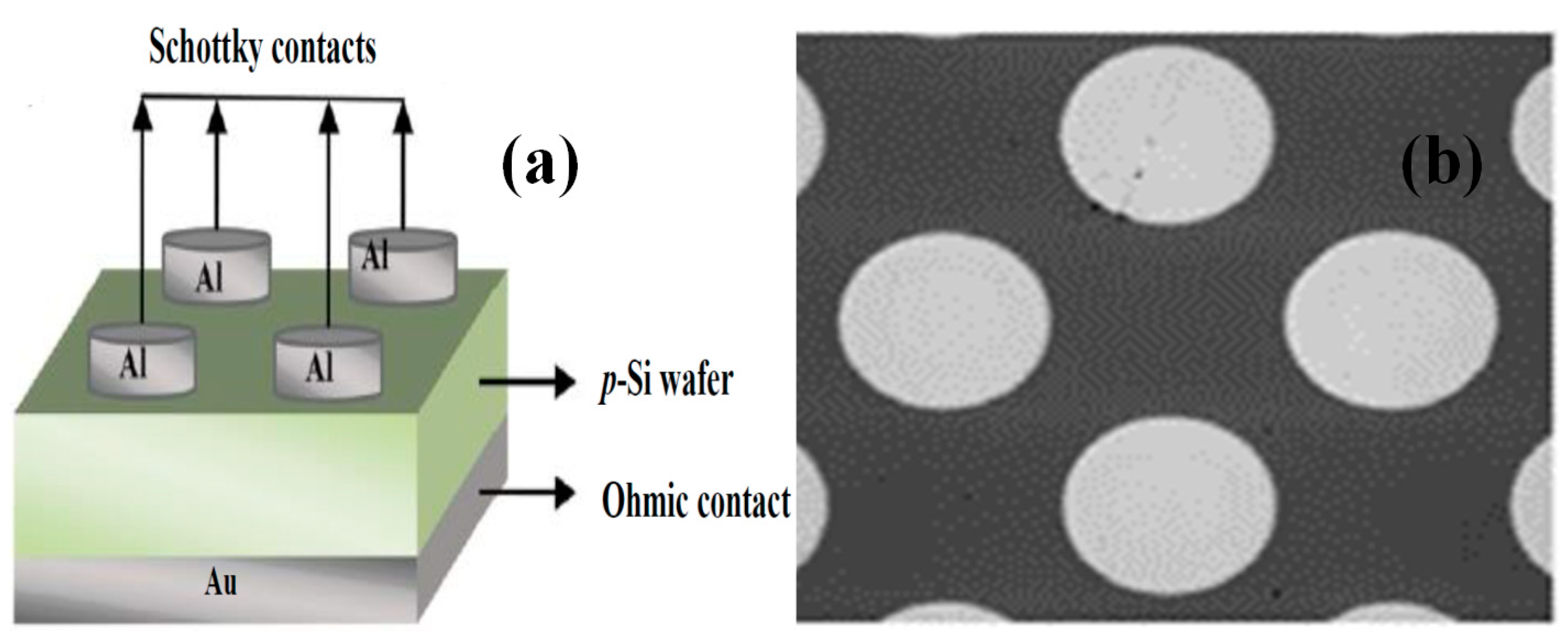
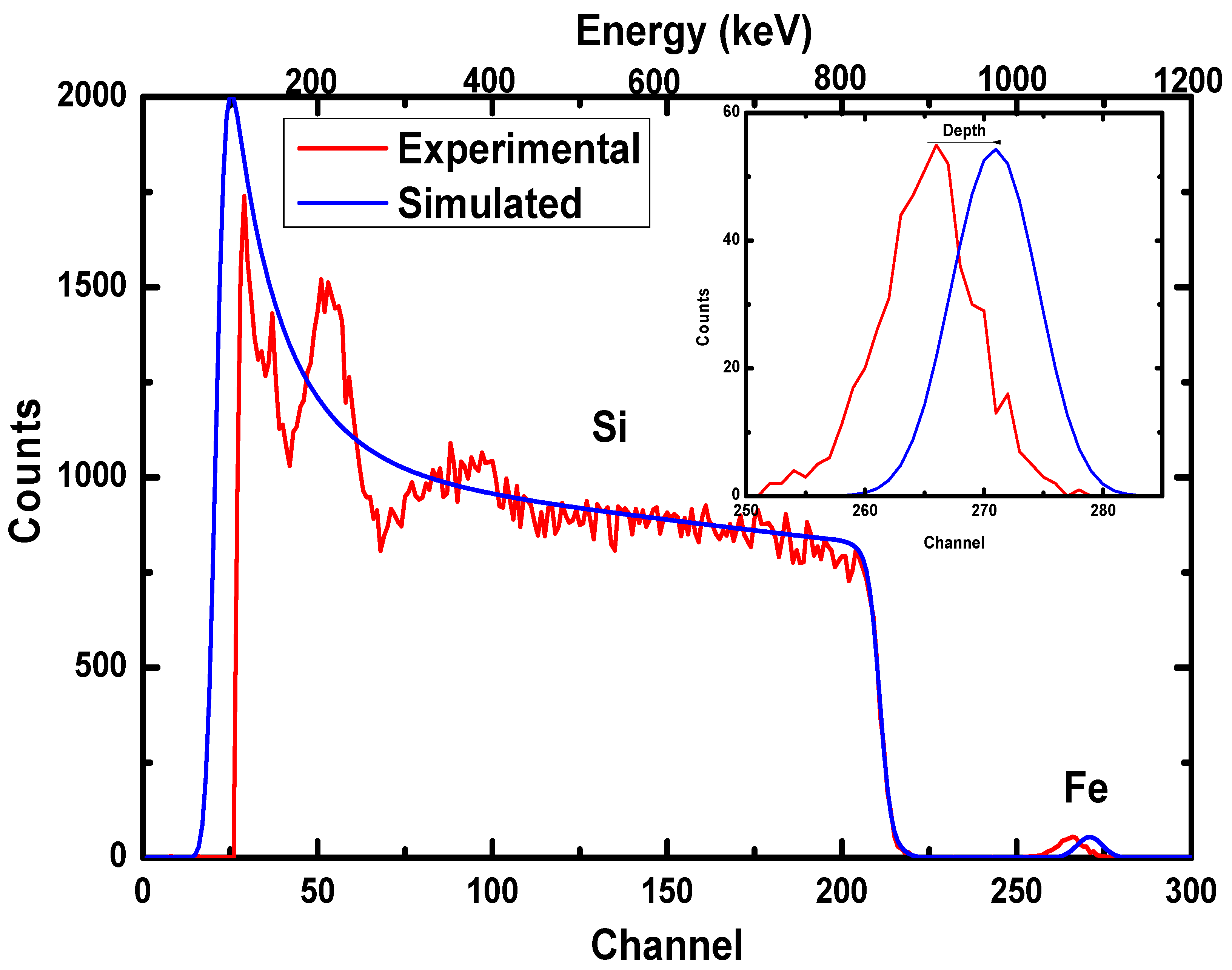
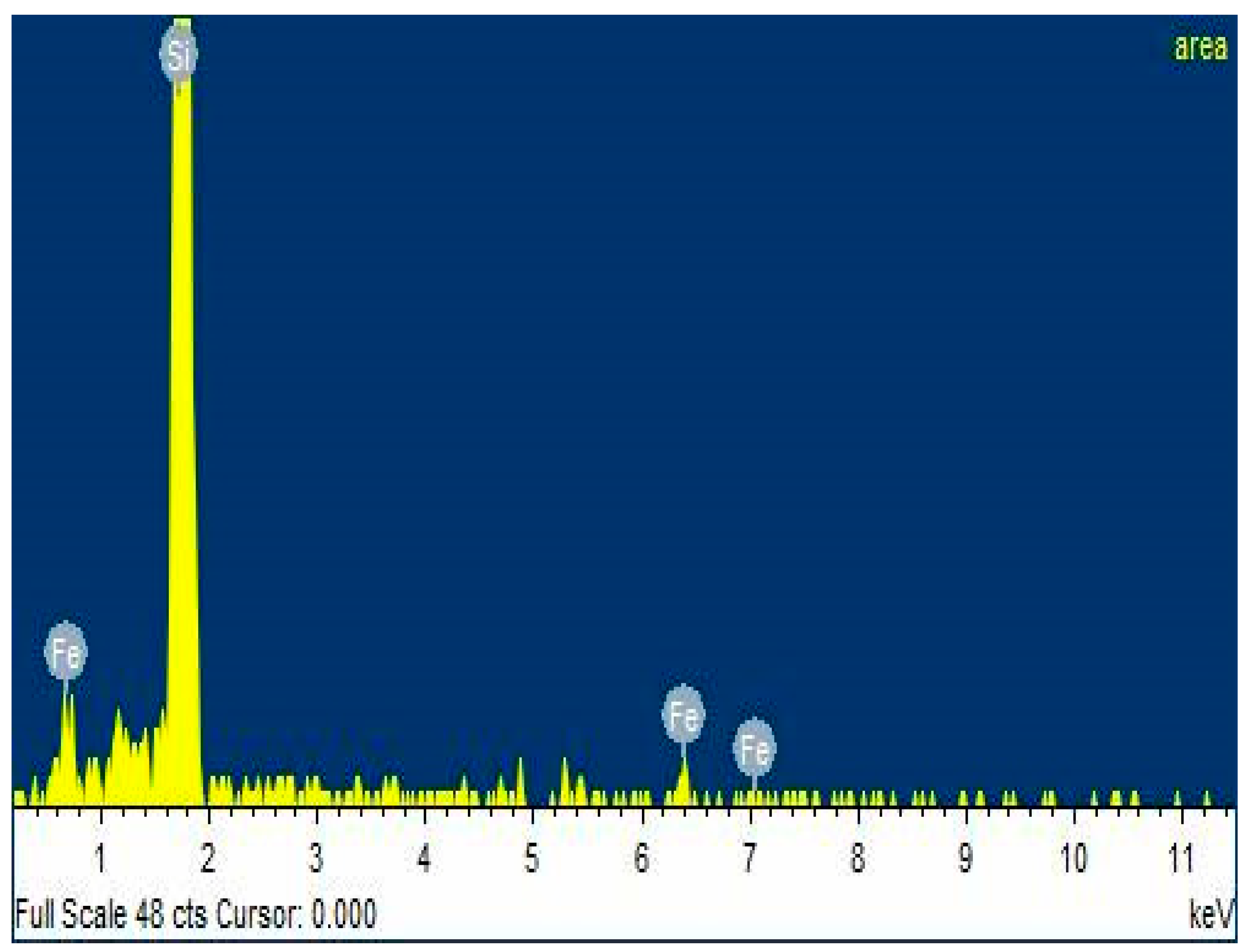
2. Details of Experiment

A p-Si (Boron-doped) wafer of resistivity 1–22 Ωcm and a thickness of 275 ± 25.0 µm was used in this work. The wafer was cut into 0.6 cm × 0.6 cm pieces. The pieces were cleaned following the standard procedure to remove handling grease and other contaminants [17] and they were immersed in 40 percent HF solution to remove the oxide layer on the surface. After the cleaning procedure, all pieces were placed in the chamber for Fe-implantation. The Fe-implantation was achieved with the aid of an ion implanter, a Varian-Extrion 200-20A2Fset-up at iThemba LABS, Johannesburg, South Africa. Fe was implanted into the polished side of the wafer at 160 keV energy to a fluence of 1.00 × 10¹⁷ ion/cm2. The chosen energy (160 keV) and fluence (1.00 × 10¹⁷ ion/cm2) are the maximum achievable setting of the set-up, which were chosen to induce high defect in the Si wafer [18]. Prior to the Fe-implantation, Stopping and Range of Ions in Matter (SRIM) 2013 simulations coded with the Transport of Ions into Matter (TRIM) program were used to predict the distribution of Fe ions in Si. The predicted implantation depth and range of the incident Fe ions in Si were observed to be 2800 Å and 1340 Å, respectively. Considering the SRIM data, it was established that the energy of 160 keV is sufficient to induce defects in Si using the Fe ions.
The elemental composition of the Fe-implanted Si material was confirmed using the RBS and EDS techniques. RBS measurements were performed on the Fe-implanted Si sample using a beam of He2+ ions of energy 3.60 MeV delivered by a 6 MeV Tandem Accelerator at iThemba LABS (Gauteng). In addition, the EDS spectrum of the Fe-implanted Si sample was acquired using a JEOL JSM 7800F Field Emission Scanning Electron Microscope (FE-SEM) equipped with an EDS situated in the Department of Physics, University of South Africa.
The SBDs were fabricated on unimplanted and Fe-implanted p-Si. Before the formation of Schottky and ohmic contacts, the pieces were cleaned again and blow-dried using nitrogen gas. A 1300 Å aluminium (Al) was evaporated and deposited through a 0.6 mm radius holes-mask on the polished side of the p-Si material to form the Schottky contact. The ohmic contact, on the other hand, was made by evaporating and depositing a 1000 Å Au layer onto the back surface of the wafers. The deposition was performed at a rate of 1 A/s at 10−6 mbar using an Edwards AUTO 306 thermal vacuum deposition system. An oxide layer of 10−30 Å thick is always available on the surface, even after etching Si wafers with an HF solution [4]. The oxide layer was not intentionally deposited. The effects of the layer on diode properties are, therefore, assumed to be common to all the diodes since they were fabricated under the same conditions. A change in diode properties would, therefore, be due to Fe-doping. A typical sample of the fabricated SBD with an Al dot representing the Schottky contact and Au as the ohmic contact, as well as the photo of the fabricated diode, are shown in Figure 1a,b.
The IV and CV data were acquired at room temperature and in a dark environment. The metres used to measure the current and capacitance were made in-house. To make sure that the electrons from tunneling overcome those from thermionic emission (TE), IV measurements were carried out from 4 to 4 V [19]. The current due to TE contributes less to the bias voltage at voltages above 0.8 V [20], and at 0.8 V, the forward current saturates as a result of the series resistance ( R s ) [21]. All through the experiments, the time between measurements was maintained for 1 s to enable the device to attain its stability. The CV measurements were taken in reverse bias from 0 to 4 V at a frequency of 18 kHz to give the deep-state carriers enough time to respond to the applied voltage [22]. This frequency was chosen after several trials that showed that the data would be unstable going below or above 18 kHz. The data was unstable because of the impact of the m-s interface on the measured capacitance. During measurements, the starting voltage was fixed at 0 V and the voltage step was maintained at 0.01 V.

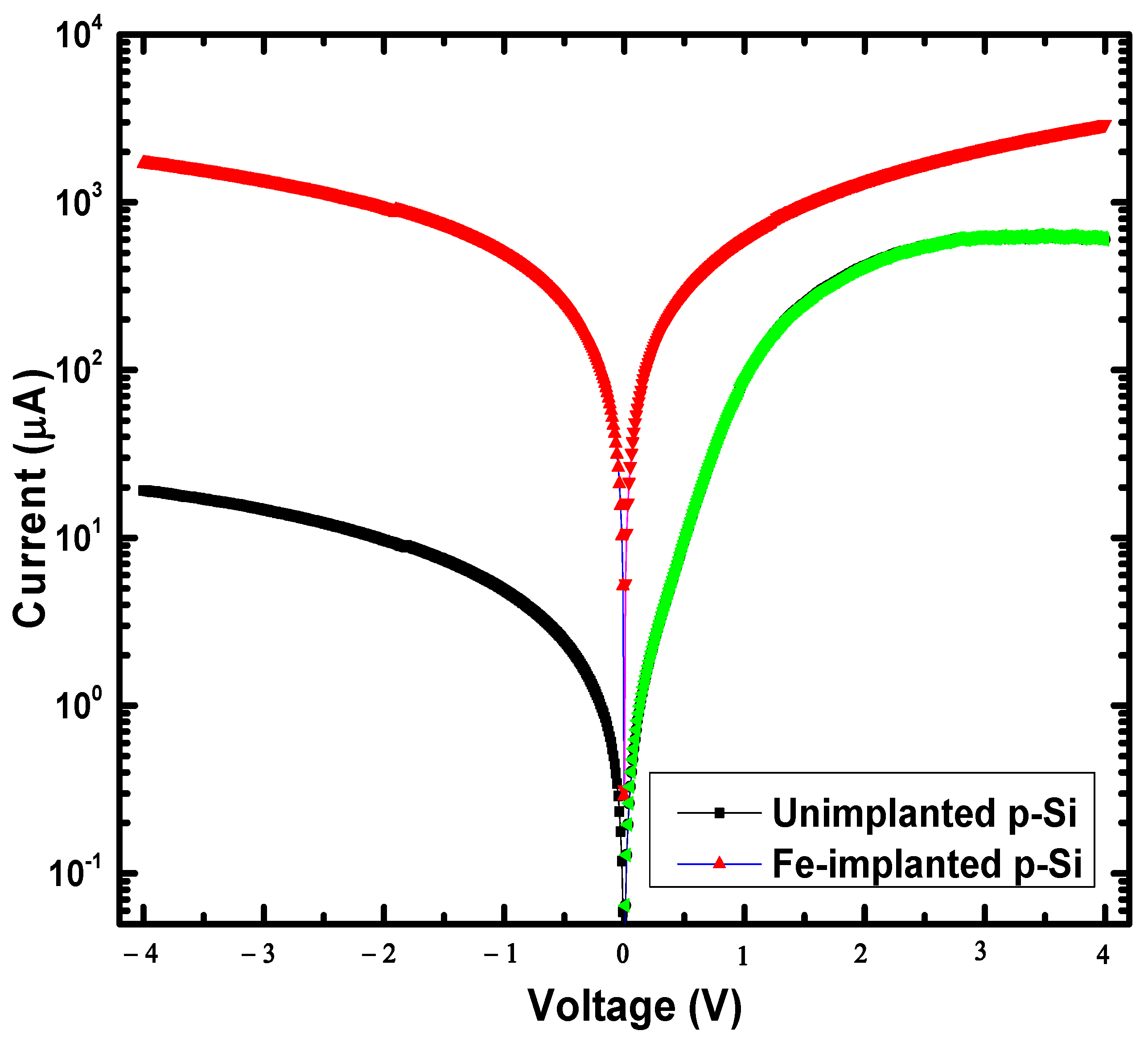
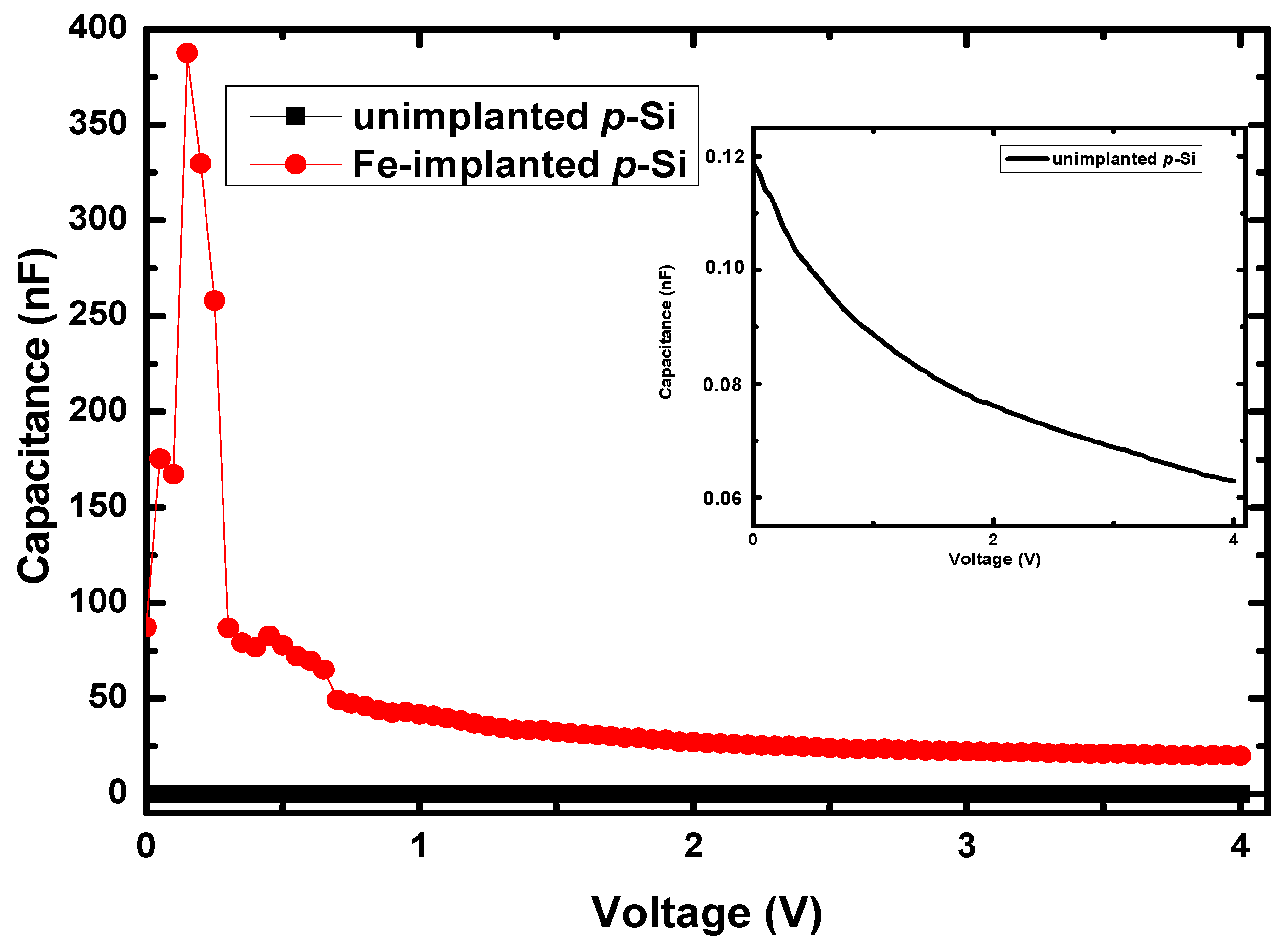
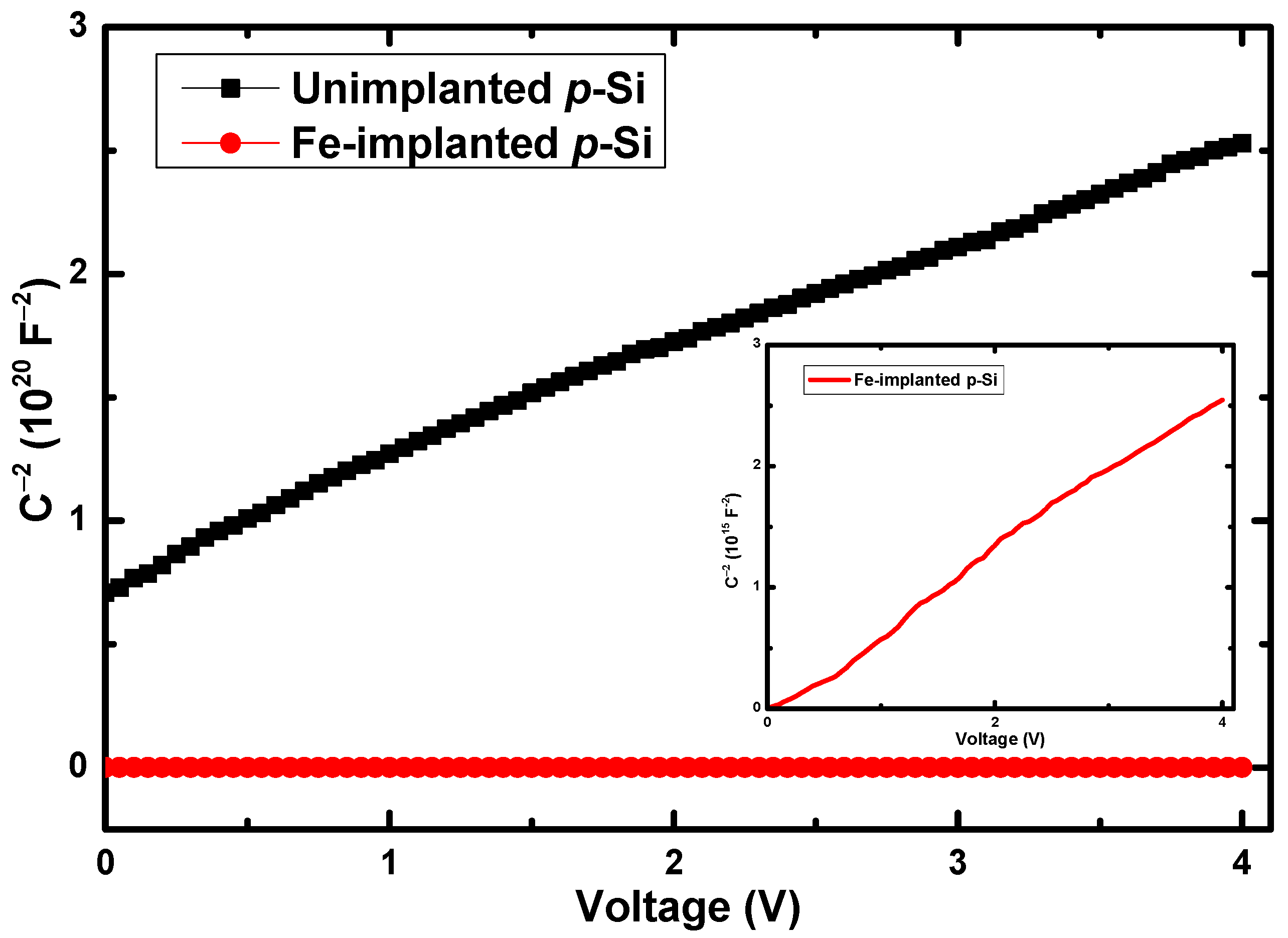
3. Results and Discussion

Figure 2 shows the RBS spectrum for the Fe-implanted Si. As shown in the figure, the experimental spectrum (red) is identical to the simulated spectrum (blue) for the Si peak. The peak of Si is well pronounced and broad, while the Fe peak is smaller. From fitting the experimental RBS spectrum, the thickness of Fe in Si was found to be 350 × 10 15 atoms / cm 2 , which is ~70.32 nm. The thickness units were converted to nm by dividing the thickness by the target density of Si, which is given as 4.977 × 10 15   atoms / cm 3 .
As seen in the inset of Figure 2, a small shift was observed in the simulated and experimental Fe peaks. Since the experimental result shifts towards low energy, it is assumed that the energies of the backscattered alpha particles are due to Fe on the surface. Therefore, as the incident ion beam penetrates Si, it loses some of its energy before colliding with Fe, which is located some depth below the surface of Si. This shift, therefore, shows that Fe was implanted at some depth from the surface of the Si. The difference in characteristic energies was used to determine this depth [23].
The penetration depth was obtained through the evaluation of the stopping power, S E and the differences in surface backscattering energy (ESurfaces) and characteristic energy (ECharacteristic). The penetration depth is given [24] as
E Characteristic E Surfaces d x = Δ x = E Characteristic E Surfaces 1 S E d E
which gives
Δ x = E Surfaces E Characteristic S E
The evaluated penetration depth of Fe in Si is 1165.90 Å. The penetration depth (1165.90 Å) obtained from RBS differs from the 2800 Å estimated using SRIM/TRIM simulation. The difference could be because in SRIM/TRIM calculations, the crystal structure and direction are not considered [25]. The influence of neighbouring atoms and the recombination of interstitial atoms with the vacancies are also not considered in the calculations [25]. In addition, during the SRIM/TRIM calculation, the dynamic composition changes of the material are not considered [26]. Furthermore, the EDS spectrum of the Fe-implanted Si sample is presented in Figure 3. The observed peaks in the EDS spectrum were Si and Fe peaks, confirming the presence of Fe in the Fe-implanted Si sample.
Figure 4 presents the semilogarithmic IV characteristics of unimplanted and Fe-implanted p-Si diodes. A linear region observed at low voltages disappears after 1 V and 0.4 V for unimplanted and Fe-implanted p-Si diodes, respectively. The linear region disappears at high voltages possibly because of R s [27,28], the interfacial insulator layer, and the interface states [27,29]. The linear region observed in the forward characteristics of the Fe-implanted p-Si diode is smaller, indicating the effects of Fe-induced defects on the R s . Furthermore, the forward and reverse current trends have increased by a factor of 5 and 102, respectively, after Fe-implantation. The increase in the current trends indicates that the Fe-induced defects generate both minority carriers (electrons) and majority carriers (holes) in p-Si material, thereby increasing the conductivity of the material.
Considering the presence of R s , the diode current is given [3] as
I = I s   exp q V I R s η k T 1
where the saturation current ( I s ) is given [3] as
I s = A A T 2 exp q ϕ B k T .
In the above equations, A (=0.00283 cm2) is the diode active area, A is the effective Richardson constant for p-type Si (=32 A cm−2 K−2) at room temperature, η is the ideality factor, k is the Boltzmann constant, T is the temperature in kelvin, q is the electronic charge, and ϕ B is the Schottky barrier height.
The ideality factor is evaluated using the slope of the linear region observed in ln(I) –V forward bias as
η = q k T d V dln I
while the saturation current ( I s ) is evaluated from the y-axis intercept. The Schottky barrier height ( ϕ B ) is evaluated [30] as
ϕ B = k T q ln A A T 2 I s .
Cheung’s plot presented in Figure 5 is employed to extract the R s , η , and ϕ B accounting for the non-linear region where the effect of R s is noticeable and is given [21,31] as
d V d ln ( I ) = η k T q + I R s
H I = V η k T q ln I A A T 2
and H I is given as
H I = η ϕ B + I R s
The value of R s is the slope of dV/dln(I)–I plot from Equation (7) and η can be calculated from the y-axis intercept. The value of η determined from Equation (7) is inserted in Equation (9) to obtain the H(I)–I plot. The slope H(I)–I plot also gives the value of R s , and the y-axis intercept is used to obtain ϕ B .
The parasitic resistance, shunt resistance ( R sh ), and R s are obtained from the plot of junction resistance R j = V I versus voltage presented in Figure 6. The maximum value of R j at a sufficiently high reverse voltage gives the R sh while the minimum value of R j in forward bias gives the R s [30,32]. Figure 6a,b presents the R j –V plots for the diodes. The R j of the unimplanted p-Si diode is independent of reverse voltage, suggesting that the SCR extends into the bulk and the material resistivity remains constant. The R j saturation is expected since the bulk of the material is relatively defect-free. The R j of the unimplanted diode decreases with forward voltage due to the high density of free carriers through the SCR. The saturation of the R j ¯ trend in the Fe-implanted p-Si diode is absent, as observed in Figure 6b. This suggests that the voltage applied is inadequate to allow all the charge carriers to pass through the SCR because of the high density of charge carriers resulting from Fe-implantation. The absence of R j saturation in both reverse and forward bias makes it not possible to extract R s and R sh for the Fe-implanted p-Si diode. However, the drastic decrease in R j suggests that parasitic resistance has decreased significantly after Fe-implantation.
The summary of diode parameters obtained using ln(I)–V and Cheung’s methods for unimplanted and Fe-implanted p-Si diodes are presented in Table 1. The η evaluated for an unimplanted p-Si diode using ln(I)–V is 2.23, while that evaluated from dV/dln(I)–I is 2.42. Both values are greater than unity, showing a non-ideal behaviour of the diode. The disparity of 0.19 observed in the values could be attributed to the different voltage regions used in the methods. Further, a value of 2.0 was reported by [33] based on the Al/SnO2/p-Si structure, which is similar to the one evaluated in our study. The η for the unimplanted p-Si diode indicates a metal-insulator-semiconductor (m-i-s) structure rather than an m-s structure, indicating that an oxide layer is present in the diode configuration [34].
The η evaluated from ln(I)–V increased after Fe-implantation, indicating that another diode conduction mechanism is involved. The η from Cheung’s method is 1.11, a value close to unity suggesting that the TE conduction mechanism dominates, despite the IV trends showing the involvement of other diode conduction mechanisms. The η close to unity observed for this diode likely illustrates that η is less reliant on defects induced in the material and hence less noticeable when the distribution of charge carriers in the bulk dominates the diode conduction mechanism.
The I s evaluated on unimplanted p-Si is 0.08 µA, which is greater than the 0.001 µA reported on Al/methyl violet/p-Si [35] and less than the 87.10 µA reported on the Au/p-Si diode [36], indicating that it is within the range of those presented in previous works. An increase in I s from 0.08 to 8.35 µA can be attributed to the increase in the density of minority carriers due to the Fe-induced defect levels in Si.
The ϕ B evaluated from ln(I)–V and H(I)–I plots for diodes fabricated on unimplanted p-Si are 0.65 and 0.77 eV, respectively. The ϕ B evaluated using H(I)–I plot is higher than the ϕ B evaluated from the ln(I)–V plot, possibly due to the different voltage regions considered when extracting the parameters. This difference was also observed in previous studies [35]. The value of ϕ B (0.65 eV) evaluated from ln(I)–V is close to the 0.68 eV reported by [37], and the value of ϕ B (0.77 eV) evaluated from H(I)–I is close to the 0.80 eV reported by [38], confirming the formation of the m-s interface during the diode fabrication process. The values of ϕ B evaluated using different methods were found to decrease after Fe-implantation. The decrease in ϕ B can be tied to an increase in I s , indicating that low energy is required to have density of charge carriers through SCR after the implantation.
The parasitic resistance ( R sh and R s ) for the unimplanted p-Si diodes are 201.00 and 4.15 kΩ, respectively. The high(low) values for R sh   R s of the diode fabricated on unimplanted p-Si evaluated from the R j –V plot confirms the perfect diode rectification behaviour [39]. The drastic decrease of R j trend after Fe-implantation is due to the high density of charge carriers generated by the Fe-induced defects. The R s evaluated using different methods differs because of the increase in the current rate as a result of the space charge injection in an electric insulating layer at the region where the voltage is high [40,41]. The discrepancy in R s values given in Table 1, therefore, suggests that there is an insulating layer formed at the m-s interface. The formed insulating layer at the interface could be SiO2 since oxygen is constantly present on the surface of Si even after the wafer has been treated chemically.
The double logarithmic IV trend of Figure 7a shows three linear regions (i, ii, and iii) with various slopes on the forward current trend of the unimplanted p-Si diode. The slopes of these regions are 1.06, 2.58, and 0.64, respectively. These regions exhibit power-law behaviour, I V m , where m is the slope [42,43]. The slope of region i, 1.06, is nearly equal to unity, suggesting that the dominant conduction mechanism is ohmic in region i. An ohmic behaviour is due to the domination of thermally generated current over the injected free carrier generated current through SCR. The slope of region ii (2.58), greater than 2, suggests that the trapped-charge-limited current (TCLC) dominates in region ii [33]. The slope of the region (0.64) shows that the current is less voltage-dependent, presumably because of the presence of R s at high voltages [22].
The double logarithmic IV trend of the Fe-implanted p-Si diode in Figure 7b shows that the forward current increases linearly for the whole voltage region with a slope of unity, indicating that an ohmic conduction mechanism dominates at the entire voltage range. Furthermore, both current trends (reverse and current trends) are equal for almost all the voltages, suggesting that the diode behaviour is ohmic. The ohmic behaviour indicates that the density of Fe-induced g-r centres is high. It has been discovered that diodes with a high ohmic region are resistant to radiation damage [8,11]. This resistance has been explained in terms of the Fermi energy being pinned at the intrinsic position such that the diode properties are independent of the incident particles [1,8,11].
The rectification ratio (RR) calculated from both diodes is used to analyse changes in rectifying behaviour due to Fe-implantation. At 4 V, the ratio of forward current to reverse current is found to be reduced from 33.61 of unimplanted to 1.65 of the Fe-implantation diode. Furthermore, Figure 7 showed an increase in both carrier densities, with the rate of increase in the density of minority carriers being higher.
Figure 8 presents the plot of reverse current ( ln I r ) against V 1 / 2 for unimplanted and Fe-implanted p-Si diode to study the conduction mechanism of the reverse current. As seen in the figure, two linear trends with different slope values were observed at low and high voltage regions on both the unimplanted and Fe-implanted p-Si diodes, suggesting that the reverse current might be clarified in terms of two different mechanisms. These mechanisms for current can be referred to as Richardson–Schottky (RS) or Poole–Frenkel (PF) emission mechanisms [44,45,46]. In RS emission, the current is given [45,47] as
I r = A A T 2 exp   ϕ b k T exp β RS V 1 / 2 k T d 1 / 2
while in PF emission, the current is given [47] as
I r = I o exp β PF V 1 / 2 k T d 1 / 2 .
In the above equations, β RS and β PF are the RS field lowering and PF coefficients, respectively, which are related [47] by
β PF = 2 β RS q 3 π ε o ε r
where ε o represents the permittivity of free space and ε r represents the relative permittivity of the material. The calculated theoretical values for β PF and β RS are 4.38 × 10 5 and 2.19 × 10 5   eV   m 1 / 2   V 1 / 2 , respectively [47]. The experimental values of β PF and β RS for unimplanted p-Si diodes are calculated by using the slope of the linear regions in Figure 8a; the β experimental value obtained from region I (0 to 0.17 V) is 4.22 × 10 5   eV   m 1 / 2   V 1 / 2 , which is closely related to the theoretical value of β PF , hence indicating that the Poole–Frenkel emission is the dominant conduction mechanism at a low voltage region. However, the β experimental value obtained from region II (0.18 to 4 V) is 1.51 × 10 5   eV   m 1 / 2   V 1 / 2 , which is closely related to the theoretical value of β RS , indicating that the Richardson–Schottky emission is the dominant conduction mechanism at the high voltage region.
The values of β PF and β RS for the Fe-implanted p-Si diode were determined experimentally by analyzing the slope of the linear regions in Figure 8b. The calculated experimental values of β from region I (0 to 0.17 V) and region II (0.18 to 4 V) are 2.12 × 10 5 and 0.13 × 10 5   eV   m 1 / 2   V 1 / 2 , respectively. These values closely align with the theoretical value of β RS , indicating that the Richardson–Schottky emission is the dominant conduction mechanism in both regions.
The CV characteristics of the unimplanted and Fe-implanted p-Si diodes are shown in Figure 9. The capacitance of the unimplanted p-Si diode decreases with applied voltage due to charge carriers being withdrawn from the SCR as voltage increases. The inset in Figure 9 presents the CV characteristics of unimplanted p-Si diodes. An absence of capacitance saturation shows that a voltage higher than 4 V is required for the SCR to be fully depleted. The capacitance trend is similar to those that are reported in past studies, confirming that our SBDs were well-fabricated [22,48] with Al as the Schottky contact.
The capacitance of the Fe-implanted p-Si diode shown in Figure 9 increased significantly, indicating that Fe generates a high density of minority carriers (electrons) in p-Si. The observed increase in saturation currents in the I-V results can be attributed to the high density of minority carriers caused by the presence of Fe. This finding supports the consistency between the IV and CV results, confirming their agreement and reliability as complementary techniques.
Furthermore, an anomalous peak is observed at a low voltage region on the CV plot of the Fe-implanted p-Si diode, indicating the Fe-induced defects start from the surface and extend to the Si bulk [49].
The C2-V plots for unimplanted and Fe-implanted p-Si diodes are presented in Figure 10. A linear region was observed on the unimplanted and Fe-implanted p-Si diodes presented in Figure 10 indicating that the doping profile is uniform. The inset in Figure 10 presents the C−2V characteristics of the Fe-implanted p-Si diode.
The capacitance, C, of an SBDs is related to the doping concentration, N A , in the semiconductor material and is given [12,22] as
C 2 = 2 V bi + V q ε s ε o A 2 N A
where V bi is the built-in potential, ε s is the dielectric constant of semiconductor material, and ε o is the permittivity in a vacuum. The relationship between the slope ( m ) and the doping concentration N A is given [22] as
N A = 2 m q A 2 ε s ε 0 .
The Schottky barrier height ( ϕ cv ) is given [12,22] as
ϕ cv = V bi + k T q ln N C N A
And the depletion region width, W D , is given [22,40] as
W D = 2 ε o ε s V d q N A .
The diode parameters such as V bi , N A , ϕ cv , and W D for the unimplanted and Fe-implanted p-Si were extracted from the linear region and are presented in Table 2.
The value of N A evaluated on an unimplanted p-Si diode is 3.41 × 10¹⁶. This value is higher than the 0.10 × 1016 cm−3 reported on the Sn/p-Si diode [46], but is close to the 1.00 × 1016 cm−3 obtained on the Au/p-Si diode [50]. The value obtained from an unimplanted diode is within the acceptable limit [50,51], confirming that the fabricated diodes are good. The value of N A increased to 224,000 × 1016 cm−3 after Fe-implantation, confirming that Fe induces defects that generate charge carriers in Si material. This increase in N A agrees with the increase in conductivity and capacitance observed in Figure 1 and Figure 6 after Fe-implantation.
The value of ϕ B that evaluated unimplanted p-Si diodes is 2.01 eV. The value is high compared to the ϕ B obtained from the I-V characteristics, as expected. The discrepancy has previously been reported in the literature by [38,52], confirming that the evaluated ϕ B is within the acceptable limit. The discrepancy was explained to be due to the interfacial native oxide layer between the metal and the semiconductor. Furthermore, the inhomogeneity of barrier height was also given as an explanation for this discrepancy [52].
The evaluated W D of an unimplanted p-Si diode is 26.6 × 10⁻⁶ cm. These values are lower than the 118 × 10−6 cm reported on Au/n-si [30] and higher than the 1.77 × 10⁻⁶ cm reported by [40], confirming that our value is within the acceptable limit reported in the reviewed literature [30,40]. The W D decreased to 0.03 × 10⁻⁶ cm after Fe-implantation, confirming the generation of charge carriers in the SCR as a result of Fe-induced defects.

4. Conclusions

The IV and CV techniques have been used to study the effect of Fe dopant on the electrical characteristics of diodes fabricated on p-Si. The results show that after Fe-implantation, the current and capacitance trends increased, indicating that charge carriers are generated as a result of Fe-implantation in p-Si, with the rate of the generation of minority carriers being higher. After Fe-implantation, the IV behaviour of the diode changed from normal exponential to ohmic, indicating that Fe induces g-r centres, which are defect levels located at the centre of the band gap of Si. The forward current of the unimplanted p-Si diode was dominated by ohmic and TCLC conduction mechanisms. However, the dominating mechanism changed to ohmic for the entire voltage region on the Fe-implanted p-Si diode. The reverse current of the unimplanted p-Si diode was dominated by the PF and RS effect while the RS effect dominated the entire voltage region of the reverse current of the Fe-implanted p-Si diode. Furthermore, the CV results show that in Si, Fe is responsible for an increase in measured capacitance, confirming that the defects induced by Fe in Si generate more minority carriers in the SCR. The results obtained from the IV and CV characteristics of the Fe-implanted p-Si diode are similar to the results shown by Au- and Pt-doped Si diodes, suggesting that Fe could be a suitable candidate in defect engineering studies.

Author Contributions

Conceptualization, J.O.B. and S.J.M.; methodology, J.O.B. and S.J.M.; formal analysis, J.O.B.; investigation, J.O.B.; resources, S.J.M. and J.O.B.; data curation, J.O.B.; writing—original draft preparation, J.O.B.; writing—review and editing, J.O.B., D.A.O. and S.J.M.; supervision, S.J.M.; All authors have read and agreed to the published version of the manuscript.

Funding

This research received no external funding, and the APC was funded by Prof. S.J.M.

Data Availability Statement

No new data were created or analyzed in this study. Data sharing is not applicable to this article.

Acknowledgments

We would like to thank Tony Miller of iThemba LABS for Fe implantation as well as D. Auret and M. Diale of the University of Pretoria for the fabrication the devices and the continued discussions on defects in solids.

Conflicts of Interest

The authors declare no conflict of interest.

References

  1. Jones, B.; Santana, J.; McPherson, M. Semiconductor detectors for use in high radiation damage environments—Semi-insulating GaAs or silicon? Nucl. Instrum. Methods Phys. Res. Sect. A Accel. Spectrometers Detect. Assoc. Equip. 1997, 395, 81–87. [Google Scholar] [CrossRef]
  2. Gurimskaya, Y.; de Almeida, P.D.; Garcia, M.F.; Suau, I.M.; Moll, M.; Fretwurst, E.; Makarenko, L.; Pintilie, I. Radiation damage in p-type EPI silicon pad diodes irradiated with protons and neutrons. Nucl. Instrum. Methods Phys. Res. Sect. A Accel. Spectrometers Detect. Assoc. Equip. 2019, 958, 162221. [Google Scholar] [CrossRef]
  3. Lutz, G. Semiconductors as Detectors. In Semiconductor Radiation Detectors; Springer: Berlin/Heidelberg, Germany, 2007. [Google Scholar] [CrossRef]
  4. Oeba, D.; Bodunrin, J.; Moloi, S. Electrical properties of 3 MeV proton irradiated silicon Schottky diodes. Phys. B Condens. Matter 2020, 610, 412786. [Google Scholar] [CrossRef]
  5. Bruzzi, M.; Adey, J.; Al-Ajili, A.; Alexandrov, P.; Alfieri, G.; Allport, P.; Andreazza, A.; Artuso, M.; Assouak, S.; Avset, B.; et al. Radiation-hard semiconductor detectors for SuperLHC. Nucl. Instrum. Methods Phys. Res. Sect. A Accel. Spectrometers Detect. Assoc. Equip. 2005, 541, 189–201. [Google Scholar] [CrossRef]
  6. Dixon, R.; Ekstrand, K. Gold and Platinum Doped Radiation Resistant Silicon Diode Detectors. Radiat. Prot. Dosim. 1986, 17, 527–530. [Google Scholar] [CrossRef]
  7. Kwon, Y.K.; Ishikawa, T.; Kuwano, H. Properties of platinum-associated deep levels in silicon. J. Appl. Phys. 1987, 61, 1055–1058. [Google Scholar] [CrossRef]
  8. McPherson, M.; Sloan, T.; Jones, B.K. Suppression of irradiation effects in gold-doped silicon detectors. J. Phys. D Appl. Phys. 1997, 30, 3028–3035. [Google Scholar] [CrossRef]
  9. Msimanga, M.; McPherson, M.; Theron, C. Fabrication and characterisation of gold-doped silicon Schottky barrier detectors. Radiat. Phys. Chem. 2004, 71, 733–734. [Google Scholar] [CrossRef]
  10. Sachse, J.-U.; Sveinbjörnsson, E.; Jost, W.; Weber, J.; Lemke, H. New interpretation of the dominant recombination center in platinum doped silicon. Appl. Phys. Lett. 1997, 70, 1584–1586. [Google Scholar] [CrossRef]
  11. Jones, B.; Santana, J.; McPherson, M. Ohmic I–V characteristics in semi-insulating semiconductor diodes. Solid State Commun. 1998, 105, 547–549. [Google Scholar] [CrossRef]
  12. Moloi, S.; McPherson, M. Capacitance–voltage behaviour of Schottky diodes fabricated on p-type silicon for radiation-hard detectors. Radiat. Phys. Chem. 2013, 85, 73–82. [Google Scholar] [CrossRef]
  13. Collins, C.B.; Carlson, R.O. Properties of silicon doped with iron or coppe. Phys. Rev. 1957, 108, 1409. [Google Scholar] [CrossRef]
  14. Graff, K.; Pieper, H. The Properties of Iron in Silicon. J. Electrochem. Soc. 1981, 128, 669–674. [Google Scholar] [CrossRef]
  15. Graff, K. Metal Impurities in Silicon-Device Fabrication; Springer Science & Business Media: Heilbronn, Germany, 2013; Volume 24. [Google Scholar]
  16. Deng, B.D.B.; Kuwano, H.K.H. Platinum as Recombination-Generation Centers in Silicon. Jpn. J. Appl. Phys. 1995, 34, 4587–4592. [Google Scholar] [CrossRef]
  17. Bera, B. Silicon wafer cleaning: A fundamental and critical step in semiconductor fabrication process. Int. J. Appl. Nanotechnol. 2019, 5, 8. [Google Scholar]
  18. Derry, T.; Lisema, L.; Magabe, A.; Aradi, E.; Machaka, R.; Madhuku, M. Allotrope conversion and surface hardness increase in ion implanted boron nitride. Surf. Coat. Technol. 2018, 355, 61–64. [Google Scholar] [CrossRef] [Green Version]
  19. Parida, M.K.; Sundari, S.T.; Sathiamoorthy, V.; Sivakumar, S. Current–voltage characteristics of silicon PIN diodes irradiated in KAMINI nuclear reactor. Nucl. Instrum. Methods Phys. Res. Sect. A Accel. Spectrometers Detect. Assoc. Equip. 2018, 905, 129–137. [Google Scholar] [CrossRef]
  20. Schroder, D.K. Semiconductor Material and Device Characterization; John Wiley & Sons: New York, NY, USA, 2015. [Google Scholar]
  21. Singh, B.K.; Tripathi, S. Fabrication and characterization of Au/p-ZnO Schottky contacts. Superlattices Microstruct. 2015, 85, 697–706. [Google Scholar] [CrossRef]
  22. Bodunrin, J.; Oeba, D.; Moloi, S. Current-voltage and capacitance-voltage characteristics of cadmium-doped p-silicon Schottky diodes. Sensors Actuators A Phys. 2021, 331, 112957. [Google Scholar] [CrossRef]
  23. Khamlich, S.; Msimanga, M.; Pineda-Vargas, C.; Nuru, Z.; McCrindle, R.; Maaza, M. Compositional analysis and depth profiling of thin film CrO2 by heavy ion ERDA and standard RBS: A comparison. Mater. Charact. 2012, 70, 42–47. [Google Scholar] [CrossRef]
  24. Wittmaack, K. Reliability of a popular simulation code for predicting sputtering yields of solids and ranges of low-energy ions. J. Appl. Phys. 2004, 96, 2632–2637. [Google Scholar] [CrossRef]
  25. Ziegler, J.F.; Biersack, J.P. The Stopping and Range of Ions in MatterTreatise on Heavy-Ion Science; Springer: Boston, MA, USA, 1985. [Google Scholar]
  26. Nordlund, K. Historical review of computer simulation of radiation effects in materials. J. Nucl. Mater. 2019, 520, 273–295. [Google Scholar] [CrossRef]
  27. Bodunrin, J.; Oeba, D.; Moloi, S. Current-voltage characteristics of iron-implanted silicon based Schottky diodes. Mater. Sci. Semicond. Process. 2021, 123, 105524. [Google Scholar] [CrossRef]
  28. Dökme, I. The effect of series resistance and oxide layer formed by thermal oxidation on some electrical parameters of Al/SiO2/p-Si Schottky diodes. Phys. B Condens. Matter 2007, 388, 10–15. [Google Scholar] [CrossRef]
  29. Altındal, Ş.; Dökme, İ.; Bülbül, M.M.; Yalçın, N.; Serin, T. The role of the interface insulator layer and interface states on the current-transport mechanism of Schottky diodes in wide temperature range. Microelectron. Eng. 2006, 83, 499–505. [Google Scholar] [CrossRef]
  30. Alialy, S.; Tecimer, H.; Uslu, H.; Altındal, Ş. A Comparative Study on Electrical Characteristics of Au/N-Si Schottky Diodes, with and without Bi-Doped PVA Interfacial Layer in Dark and Under Illumination at Room Temperature. J. Nanomed. Nanotechnol. 2017, 4, 1000167. [Google Scholar] [CrossRef]
  31. Cheung, S.K.; Cheung, N.W. Extraction of Schottky diode parameters from forward current-voltage characteristics. Appl. Phys. Lett. 1986, 49, 85–87. [Google Scholar] [CrossRef]
  32. Soliman, H.; Farag, A.; Khosifan, N.; Solami, T. Electronic and photovoltaic properties of Au/pyronine G(Y)/p-GaAs/Au:Zn heterojunction. J. Alloys Compd. 2012, 530, 157–163. [Google Scholar] [CrossRef]
  33. Dökme, I.; Altindal, Ş. On the intersecting behaviour of experimental forward bias current–voltage (IV) characteristics of Al/SiO2/p-Si (MIS) Schottky diodes at low temperatures. Semicond. Sci. Technol. 2006, 21, 1053–1058. [Google Scholar] [CrossRef]
  34. Güllü, Ö.; Aydoğan, Ş.; Biber, M.; Türüt, A. Fabrication and electrical properties of Al/phenolsulfonphthalein/n-Si/AuSb structure. Vacuum 2008, 82, 1264–1268. [Google Scholar] [CrossRef]
  35. Güllü, Ö.; Çankaya, M.; Biber, M.; Türüt, A.B. Gamma irradiation-induced changes at the electrical characteristics of organic-based schottky structures. J. Phys. D Appl. Phys. 2008, 41, 135103. [Google Scholar] [CrossRef]
  36. Moloi, S.; McPherson, M. Current–voltage behaviour of Schottky diodes fabricated on p-type silicon for radiation hard detectors. Phys. B: Condens. Matter 2009, 404, 2251–2258. [Google Scholar] [CrossRef]
  37. Sağlam, M.; Korucu, D.; Türüt, A. The effects of the time-dependent on the characteristic parameters of polypyrrole/p-type Si/Al diode. Polymer 2004, 45, 7335–7340. [Google Scholar] [CrossRef]
  38. Ocak, Y.; Kulakci, M.; Kılıçoğlu, T.; Turan, R.; Akkılıç, K. Current–voltage and capacitance–voltage characteristics of a Sn/Methylene Blue/p-Si Schottky diode. Synth. Met. 2009, 159, 1603–1607. [Google Scholar] [CrossRef]
  39. Taşçıoğlu, İ.; Aydemir, U.; Altındal, Ş.; Kınacı, B.; Özçelik, S. Analysis of the forward and reverse bias I-V characteristics on Au/PVA:Zn/n-Si Schottky barrier diodes in the wide temperature range. J. Appl. Phys. 2011, 109, 054502. [Google Scholar] [CrossRef]
  40. Yahia, I.; Zahran, H.; Alamri, F.; Manthrammel, M.A.; AlFaify, S.; Ali, A.M. Microelectronic properties of the organic Schottky diode with pyronin-Y: Admittance spectroscopy, and negative capacitance. Phys. B Condens. Matter 2018, 543, 46–53. [Google Scholar] [CrossRef]
  41. Bodunrin, J.; Moloi, S. Electrical properties and conduction mechanisms of heavily iron implanted silicon diodes. Solid State Commun. 2022, 341, 114575. [Google Scholar] [CrossRef]
  42. Rao, L.D.; Reddy, V.R. Electrical parameters and series resistance analysis of Au/Y/p-InP/Pt Schottky barrier diode at room temperature. In Proceedings of the AIP Conference Proceedings, Uttar Pradesh, India, 21–25 December 2015; AIP Publishing LLC: Melville, NY, USA, 2016; Volume 1731, p. 120020. [Google Scholar] [CrossRef]
  43. Bodunrin, J.O.; Moloi, S.J. Current-Voltage Characteristics of 4 MeV Proton-Irradiated Silicon Diodes at Room Temperature. Silicon 2022, 14, 10237–10244. [Google Scholar] [CrossRef]
  44. El-Nahass, M.; Ali, H. Temperature dependent I–V characterization of Coronene/p-Si based heterojunctions: Space charge limited current, Schottky emission at high voltages, thermionic emission and pool-Frenkel emission at low voltages. Solid State Sci. 2020, 106, 106297. [Google Scholar] [CrossRef]
  45. Ali, H.; Soliman, H.; Eid, K.; Atef, S. Electrical transport mechanisms and photovoltaic behavior of 2-(2-furanylmethylene) propanedinitrile/p-Si heterojunction. Mater. Chem. Phys. 2013, 142, 132–137. [Google Scholar] [CrossRef]
  46. Aldemir, D.A.; Kökce, A.; Özdemir, A.F. Temperature effects on the electrical characteristics of Al/PTh-SiO2/p-Si structure. Bull. Mater. Sci. 2017, 40, 1435–1439. [Google Scholar] [CrossRef] [Green Version]
  47. Muhammad, F.; Tahir, M.; Zeb, M.; Kalasad, M.N.; Said, S.M.; Sarker, M.R.; Sabri, M.F.M.; Ali, S.H.M. Synergistic enhancement in the microelectronic properties of poly-(dioctylfluorene) based Schottky devices by CdSe quantum dots. Sci. Rep. 2020, 10, 4828. [Google Scholar] [CrossRef] [Green Version]
  48. Şahin, B.; Çetin, H.; Ayyildiz, E. The effect of series resistance on capacitance–voltage characteristics of Schottky barrier diodes. Solid State Commun. 2005, 135, 490–495. [Google Scholar] [CrossRef]
  49. Altındal, Ş.; Uslu, H. The origin of anomalous peak and negative capacitance in the forward bias capacitance-voltage characteristics of Au/PVA/n-Si structures. J. Appl. Phys. 2011, 109, 074503. [Google Scholar] [CrossRef]
  50. Yeganeh, M.A.; Rahmatollahpur, S.H. Barrier height and ideality factor dependency on identically produced small Au/p-Si Schottky barrier diodes. J. Semicond. 2010, 31, 74001. [Google Scholar] [CrossRef]
  51. Güllü, Ö.; Demir, F.; Cimilli, F.E.; Biber, M. γ-Irradiation-induced changes at the electrical characteristics of Sn/p–Si Schottky contacts. Vacuum 2007, 82, 789–793. [Google Scholar] [CrossRef]
  52. Çakar, M.; Yıldırım, N.; Karataş, Ş.; Temirci, C.; Türüt, A. Current-voltage and capacitance-voltage characteristics of Sn/rhodamine-101∕n-Si and Sn/rhodamine-101∕p-Si Schottky barrier diodes. J. Appl. Phys. 2006, 100, 074505. [Google Scholar] [CrossRef]
Figure 1. The fabricated diode showing Al as the Schottky contact and Au as the ohmic contact (a), as well as a photo of the fabricated diode (b).
Electronicmat 04 00008 g001
Figure 2. RBS spectra of Fe-implanted Si material to the fluence of 1017 (d) ion/cm2.
Electronicmat 04 00008 g002
Figure 3. EDS spectra of Fe-doped Si material to the fluence of 1017 (d) ion/cm2.
Electronicmat 04 00008 g003
Figure 4. ln(I)–V behaviour of SBDs fabricated on unimplanted and Fe-implanted p-Si at room temperature.
Electronicmat 04 00008 g004
Figure 5. dV/dln(I)–I plot (a) and H(I)–I plot (b) of the SBDs fabricated on unimplanted and Fe-implanted p-Si.
Electronicmat 04 00008 g005
Figure 6. R j V plot for unimplanted (a) and Fe-implanted (b) p-Si diode.
Electronicmat 04 00008 g006
Figure 7. IV behaviour of the SBDs fabricated on unimplanted (a) and Fe-implanted (b) p-Si in a double logarithmic scale.
Electronicmat 04 00008 g007
Figure 8. ln (Ir)–V1/2 characteristics of the SBDs fabricated on unimplanted (a) and Fe-implanted (b) p-Si in a double logarithmic scale. i: region I, ii: region II.
Electronicmat 04 00008 g008
Figure 9. C-V characteristics of diodes fabricated on unimplanted and Fe-implanted p-Si at a measurement frequency of 18 kHz. Inset: rescaled C-V characteristics of diodes fabricated on unimplanted p-Si.
Electronicmat 04 00008 g009
Figure 10. C−2V characteristics of diodes fabricated on unimplanted and Fe-implanted p-Si at a frequency of 18 kHz. Inset: rescaled C−2V characteristics of diodes fabricated on Fe-implanted p-Si.
Electronicmat 04 00008 g010
Table 1. Diode parameters obtained from different methods for SBDs fabricated on unimplanted and Fe-implanted p-Si.
ln(I)–VdV/dln(I)–IH(I)–I
p-Si η I s ( μ A ) ϕ B ( eV ) R s   ( k ) η R s   ( k ) ϕ B ( eV )
Unimplanted2.230.080.650.482.423.010.77
Fe-implanted2.898.350.540.241.111.330.73
Table 2. V plots for unimplanted and Fe-implanted p-Si diodes.
p-Si Diode V b i   ( V ) N A   ( 10 16   cm 3 ) ϕ c v   ( eV ) W D   ( 10 6   cm )
Unimplanted1.843.412.0126.6
Fe-implanted0.09224,0000.030.03
Disclaimer/Publisher’s Note: The statements, opinions and data contained in all publications are solely those of the individual author(s) and contributor(s) and not of MDPI and/or the editor(s). MDPI and/or the editor(s) disclaim responsibility for any injury to people or property resulting from any ideas, methods, instructions or products referred to in the content.

