1. Introduction
In the recent past, ultraviolet (UV) photodetectors (PDs) have been explored for various applications, such as optical wireless communication, flame sensors, and medical inspection systems, etc. [
1]. Recent reports indicate that UV radiation has enormous potential in the area of sterilization and disinfection, electronics, biomedicine, air purification, etc. However, high levels of UV radiation may cause a considerable increase in the incidence rate of skin cancer [
2,
3]. Because of this, extensive efforts are invested by researchers in the area of UV photodetection technology. A UV photodetection device can convert UV radiation into electrical signals based on the photoelectric effect. Thus, the development of UV photodetection devices has attracted significant attention from researchers worldwide. Silicon (Si)-based photodetectors are commercially available; however, Si is an indirect bandgap semiconductor (1.1 eV) that requires a high-pass optical filter to stop the high-energy photons [
4]. As a corollary, it increases the cost and complexity of the device. In addition, Si-based optoelectronic devices are prone to degradation when exposed to optical signals with energies higher than their band gap energy, which hinders the utility of these PDs for UV detection [
5]. Thus, UVPDs based on direct and large band gap semiconductor materials, such as BN, Ga
2O
3, GaN, ZnO, and SnO
2, etc., are sought when ultraviolet light detection is desired [
5]. Among the wide band gap materials, GaN is the most suitable material for UVPD due to its lowest excitation binding energy, which leads to electron–hole separation easily under light illumination [
6]. Additionally, GaN-based UVPD can be operable in hostile environmental conditions such as high pressure, harsh radiation, high temperatures, etc.
To fabricate an efficient UVPD device, a comprehensive understanding of the different aspects that affect the optical and electrical transport properties of thin films is required. The major bottleneck in developing highly efficient GaN/AlN heterostructure-based devices is the crystalline quality, surface morphology (higher aspect ratio), lower optical defects, and efficient optoelectrical transport, which directly affect light–matter interactions and influence the current transport behavior of the device. Recently, for the large-scale production and high-quality fabrication of GaN-based devices, Si substrates have been employed to grow epitaxial GaN layers [
7]. Furthermore, the direct growth of GaN on a Si substrate may lead to insignificant cracks and defects on the surface owing to the thermal expansion coefficients and lattices mismatched between the Si and the epitaxial GaN. Therefore, incorporating a buffer layer is vital since it enhances the crystalline quality and decreases surface stress states in epitaxial GaN films [
8]. Additionally, the buffer layer influences the surface morphology (a critical factor in high light–matter interactions) of the epitaxial film. Many studies discuss synthesizing GaN on Si with an AlN buffer layer [
9]. Additionally, the epitaxial GaN/AlN/Si growth, which has been extensively studied in earlier reports, can be controlled by modulating the growth parameters of the AlN buffer layer (such as growth temperature, Al flux, nitrogen plasma power, and growth time) [
10,
11,
12,
13]. However, the influence of the AlN buffer layer temperatures on the morphology of the epitaxial GaN/AlN/Si heterostructure needs to be explored, which significantly influences the device performance.
In this work, we grew various epitaxial GaN/AlN heterostructures at different buffer layer temperatures and observed that the AlN grown at 770 °C was more stress relaxed than those grown at higher temperatures, leading to the unique nano-obelisk GaN-like morphology. Further, the MSM detector devices were developed to investigate the effects of AlN buffer layers on the optoelectronic characteristics of GaN-based UVPD. The nano-obelisk GaN-based device performed significantly well, realized a higher gain in their performance parameters, and demonstrated a responsivity of 118 AW−1. This report strengthens the concept of enhancing the performance of GaN-based UVPD devices by improving the quality of the grown film via the intervention of a suitable AlN buffer layer, motivating the development of next-generation UVPDs.
2. Experimental
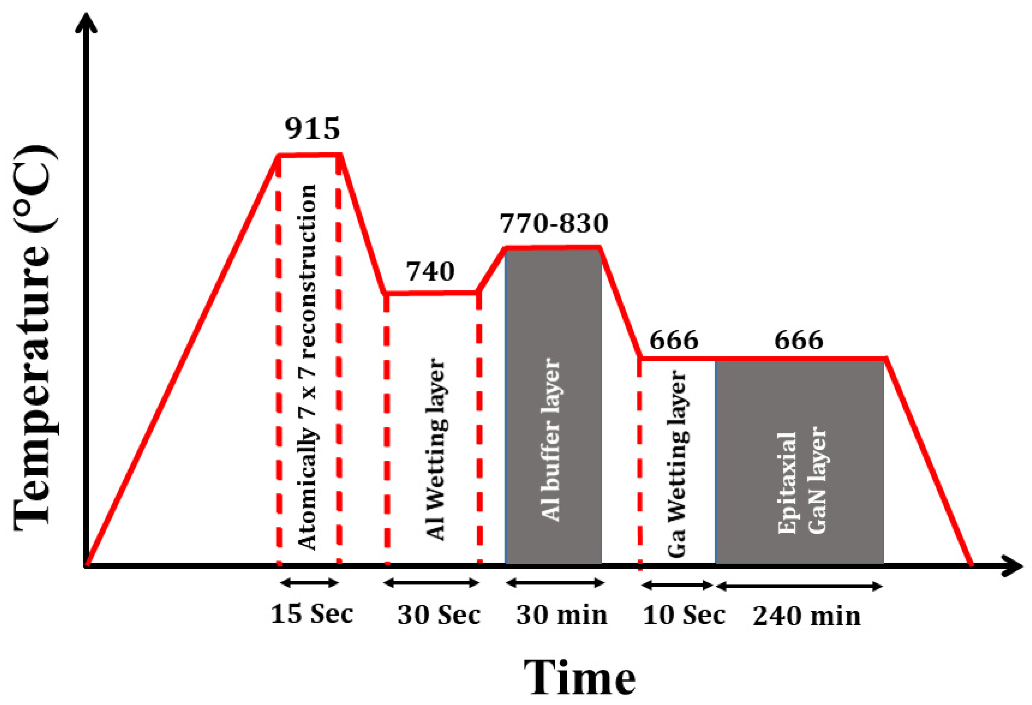
The GaN/AlN heterostructures were grown on a Si (111) substrate by a Radio-Frequency Plasma-assisted Molecular beam epitaxy (RF-PAMBE Compact 21, Riber, France) system having a base pressure in the order of 10
−11 Torr. Before loading into the load-lock chamber, the silicon substrates were chemically precleaned using the standard RCA procedure [
14], followed by out-gassing in the buffer chamber at 630 °C. Afterward, the Si substrate was flash heated at 915°C in the growth chamber to achieve an atomically clean 7 × 7 reconstructed surface. Initially, the AlN buffer layer was grown on a Si (111) substrate after depositing the Al wetting layer as the nucleation seed layer. The AlN buffer layer can reduce the tensile stress in the GaN films grown on the Si substrate, leading to crack-free growth [
5]. A growth–temperature vs. time diagram with each step involved in the growth process is shown in
Figure 1. The AlN films were developed at different substrate temperatures, such as 770 °C, 800 °C, and 830 °C while keeping all other growth parameters constant during the GaN/AlN heterostructure growth to comprehend the function of the AlN buffer layer. The substrate temperature; beam equivalent pressure of Ga, N
2 flux, and RF power; and growth span during GaN growth was set to 666 °C, 2.8 × 10
−6 Torr, 3 sccm, 400 W, and 240 min, respectively. Below 760 °C, the surface of the inert Al metal still exists. As a result, all AlN growth in this work was carried out at T ≥ 770 °C [
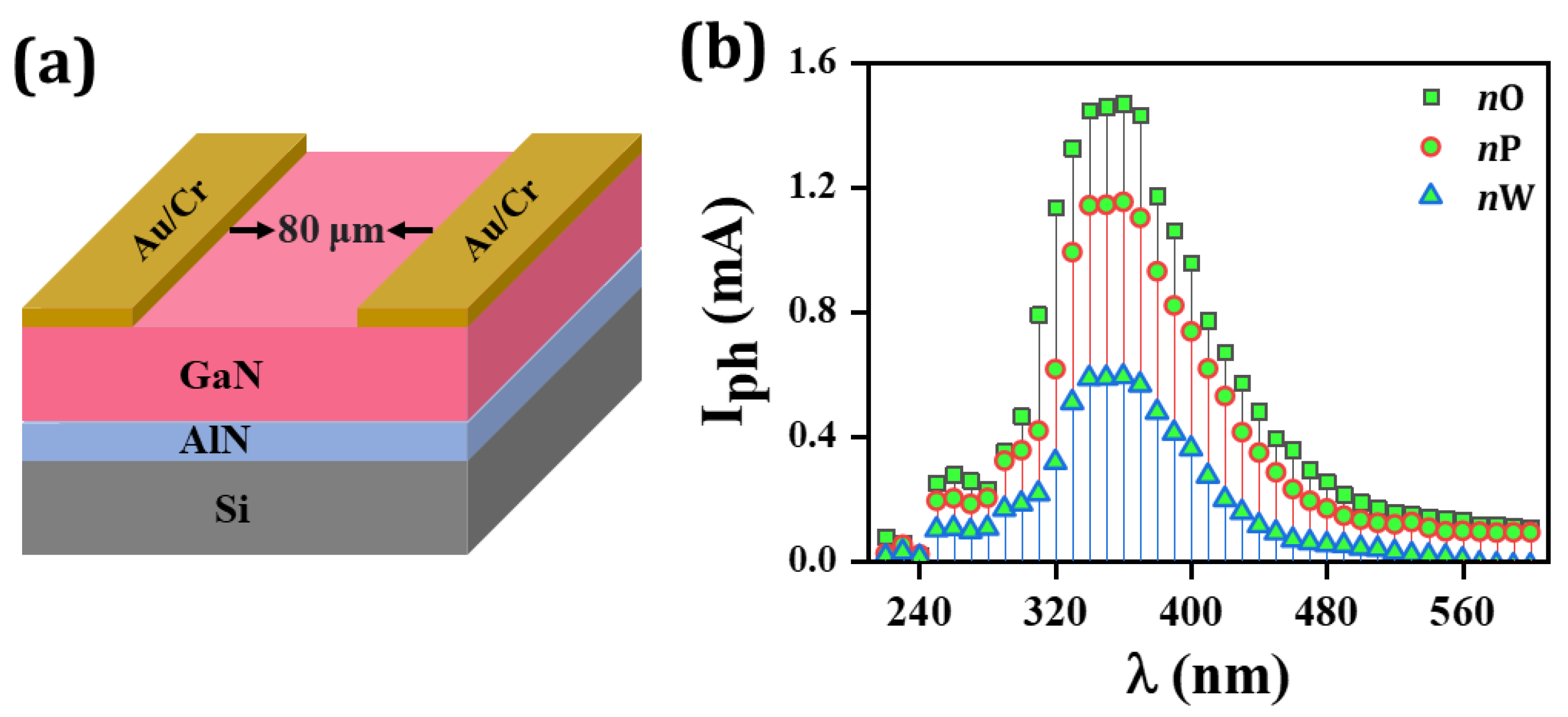
8]. The in situ real-time growth monitoring was performed using the Reflection high-energy electron diffraction (RHEED) technique with a STAIB electron gun operating at 12 KeV. The growth with a distinct AlN buffer led to the formation of various structures of GaN labeled as nano-obelisk (nO), nanopyramid (nP), and nano wax/wane (nW) for AlN grown at 770 °C, 800 °C, and 830 °C, respectively. The labeling of the samples was due to the archive’s different morphology, which is discussed in the FESEM analysis part of the report.
The structural quality of the grown heterostructure was determined using PANalytical X’Pert PRO MRD System High-resolution X-ray diffraction (HRXRD) using CuKα1 radiation (λ = 1.5406 A°). A room temperature (RT) photoluminescence (Edinburgh Instruments FLS-980 D2D2) measurement was also performed with the IK series He-Cd (Kimmon) laser as an excitation source of a 325 nm wavelength for the investigation of the optical properties of the grown films. Further, morphological studies were carried out using field-emission scanning electron microscopy (FESEM, FEI Verios 460L). Cr/Au metal electrodes with a thickness of 10/90 nm and an 80 µm spacing were deposited using a shadow mask in a thermal evaporation system to build a 2-terminal metal–semiconductor–metal (MSM) PD device. The photo response measurements were performed using a probe station that included an S10 Triax probe station and a source meter Keithley-2401 as an acquisition unit, 450 W Xenon Lamp, and a 325 nm solid-state diode laser source.
3. Results and Discussion
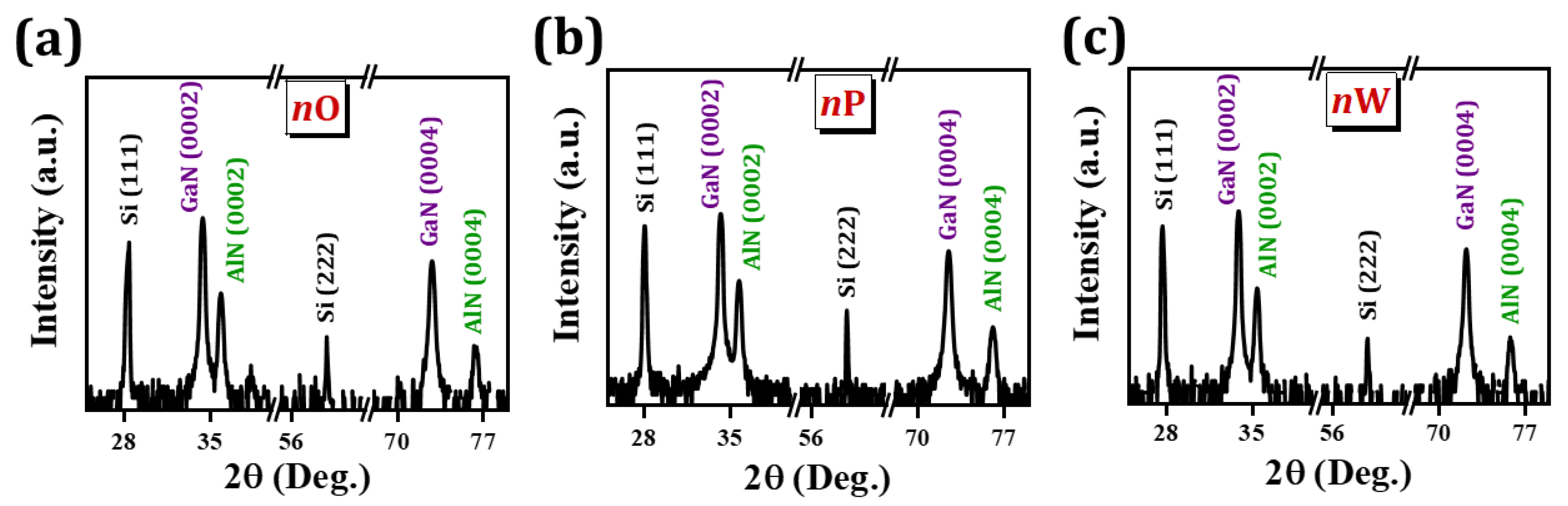
An HRXRD technique was used to examine the structural properties of the grown heterostructures. The HRXRD 2θ scan is shown in
Figure 2 for all three grown GaN/AlN/Si heterostructures. The peaks at around 34.5 and 72.9 correspond to the (0002) and (0004) planes of GaN [
15]. The sharp peaks at 28.4 ± 0.01° and 58.8 ± 0.01° were derived from the first- and second-order diffractions of Si, identified as the peak corresponding to Si (111) and Si (222), which confirms the presence of the Si substrate. Before every HRXRD measurement, the position of the silicon peak was optimized. Therefore, the observed shift in the AlN (0002) plane of the grown heterostructure was directly related to the material quality of the AlN and not due to detector alignment. The comprehensive structural analysis of the grown heterostructures can be found elsewhere [
5,
16]. From the XRD spectra, the AlN (0002) peak position was observed at 35.88°, 35.72°, and 35.44° for nO, nP, and nW, respectively. Utilizing Bragg’s law equations [
17], the lattice constant values were calculated as 0.4998 nm, 0.5032 nm, and 0.5059 nm for the nO, nP, and nW structures, respectively. The lattice constant value of 0.4998 nm was found to be in close agreement with a well-reported value of a lattice strain-free AlN (0.4982 ± 0.0002 nm) [
18]. However, the observation revealed that the lattice constant value increased with the increase in the buffer layer temperature. Further, the lattice strain existing in the grown structure was calculated using the obtained lattice parameters with the help of the following equation:
where Co denotes the lattice strain-free AlN film lattice constant, and C denotes the lattice constant of the grown AlN. The attained values of the biaxial lattice strain in AlN film in the heterostructure were found to be 0.32%, 0.95%, and 1.50% for the heterostructure grown at the buffer layer temperatures 770 °C, 800 °C, and 830 °C, respectively. The lattice constant value close to the strain-free AlN in the nO structure had a reduced lattice strain value of 0.32%, leading to better AlN growth in the heterostructure. As the growth temperature of the buffer layer increased, a higher strain value was found in the grown AlN.
Moreover, the estimated lattice strain of the buffer layer was further utilized to evaluate the stress [
19] using the below-given relation:
where σ is the tensile stress, M = 140 GPa is Young’s modulus of the silicon substrate, and ɛ is the obtained lattice strain. The calculated stress for nO (nP and nW) was 0.45 GPa (1.33 GPa and 2.10 GPa). The analysis revealed that 770 °C was the optimal growth temperature for AlN, the buffer layer, estimated as the lowest stress (0.45 GPa) for nO. Additionally, the optical and morphological properties were also explored to observe the impact of the buffer layer in the GaN/AlN heterostructure.
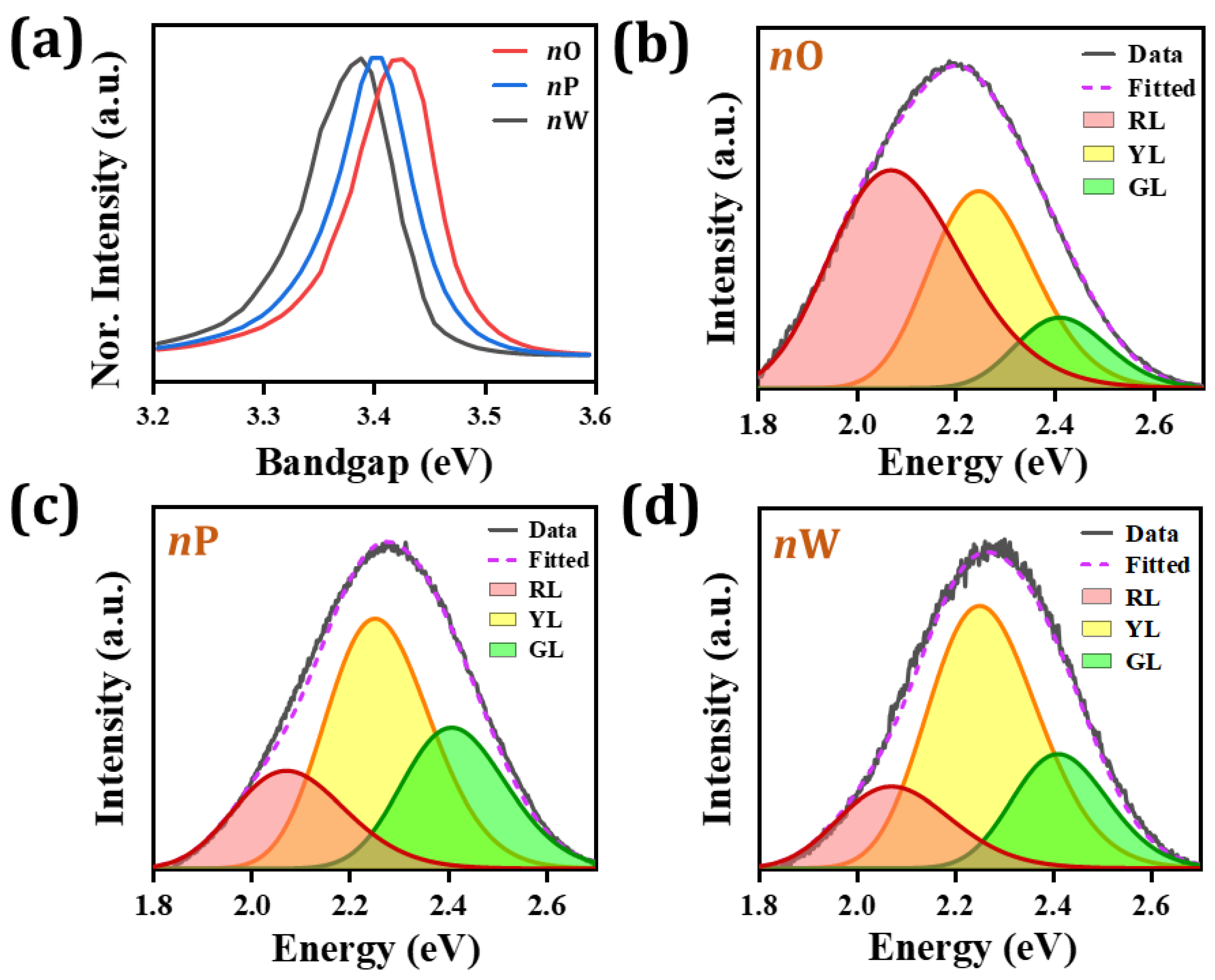
Photoluminescence (PL) spectroscopy was used to obtain detailed information similar to the transition in optical states and surface stress. The observed PL spectra were separated into two categories, sharp near-band emissions (NBEs) and broad defect peaks. The NBE peak is attributed to the radiative transition from the conduction band to the valence band representing the bandgap energy of the grown film.
Figure 3a shows an enlarged NBE region of the PL spectra. The intense near bandgap transitions of nO, nP, and nW was located at 3.42 eV, 3.40 eV, and 3.38 eV, respectively, while for the unstrained GaN layer, the near bandgap transition was located at 3.4285 eV. The peak shift in the NBE is related to the surface biaxial stress of the film, which can be calculated using the following equation [
19]:
where Eg is the intense near bandgap transition. The surface biaxial stresses of the heterostructure nO, nP, and nW were calculated to be about 0.403 GPa, 1.35 GPa, and 2.29 GPa, respectively. This indicates the presence of surface biaxial stress as tensile stress in all the grown films, while the minimum surface biaxial stress was obtained in nO. The detailed PL analysis demonstrated that a high-quality GaN film with good optical properties was grown at 770 °C. Further, the AlN buffer layer stress calculated by the HRXRD was approximately the same as the surface stress calculated by the PL spectra. This indicates that the AlN buffer layer played an important role in obtaining quality GaN film growth, as the AlN buffer layer can tune the surface stress of the GaN epitaxial layer.
Additionally, the broad PL peak represents the defect states present in the grown heterostructure. The defect-correlated broadband spectra with the deconvoluted defect states labeled as red luminescence (RL), yellow luminescence (YL), and green luminescence (GL) of nO, nP, and nW are shown in
Figure 3b–d, respectively. The GL and RL bands are perceived due to the combination of excess metal and oxygen impurities bound to dislocations that provide localized occupation to the charge carriers [
16]. The presence of YL emissions is an effect of the deep acceptor level that is developed because of gallium vacancy analogous optical defects in undoped GaN [
20]. Further,
Table 1 illustrates the variance in each defect peak for GaN synthesized on various temperature-modulated AlN buffer layers. Notably, the contribution of the RL peak with a center at 2.1 eV dropped from 56.2% to 22.1% for nO to nW. However, the YL contribution increased from 34.4% to 58.5%. Therefore, GL adopted a nonsymmetric trend.
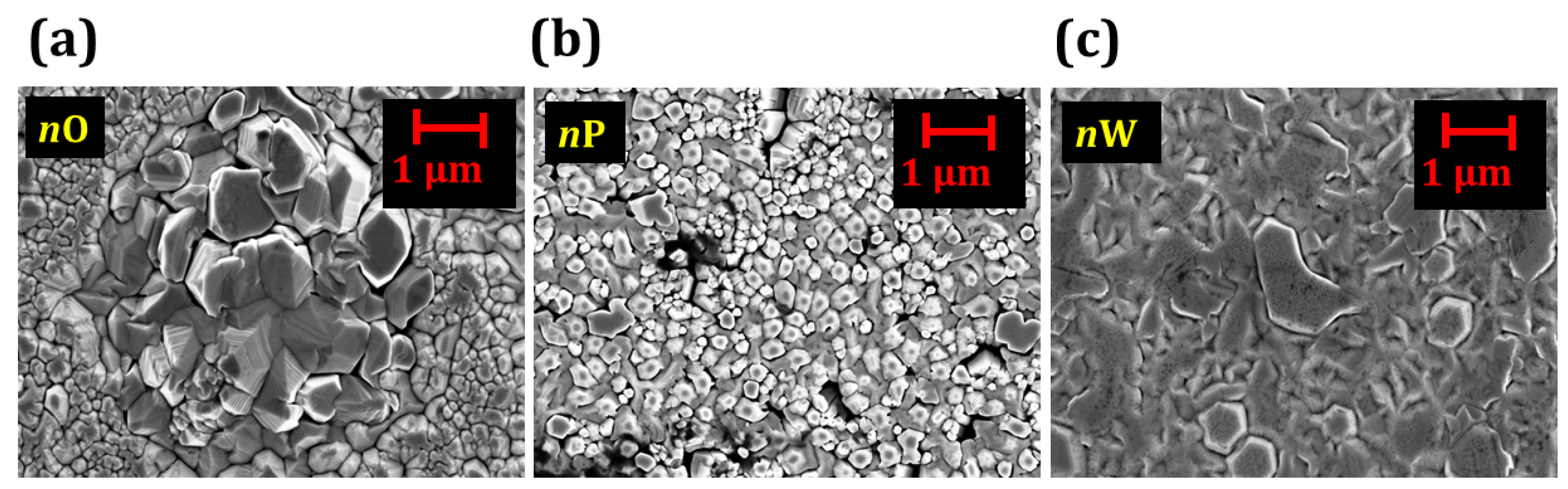
Further, to understand the impact of stress on the morphology of the grown heterostructure, the FESEM image of all three heterostructures is shown in
Figure 4. The top view of nO is shown in
Figure 4a, revealing its nano-obelisks-like morphology. In comparison,
Figure 4b reveals a hexagonal-shaped nanopyramidal structure, while
Figure 4c displays agglomerated terraces-assisted wax/wane, and the GaN structure belongs to nW. Further, the calculated crystallized size that was obtained using ImageJ software for nO, nP, and nW were found to be 80 nm, 119 nm, and 189 nm, respectively, and the mean size histogram is shown in
Figure S1, Supporting Information (SI). This agglomerated surface might have resulted from the maximum surface stress obtained in nW. The examined morphological differences via FESEM microscopy revealed that the grown GaN films with a planner surface were almost featureless in the nW structure, with poorly defined domains and nonoptimal phase segregation, which is usually not ideal for charge transport. For optoelectronic applications, however, a larger surface area is always preferable because a large surface leads to a higher light–matter interaction. The surface of nO and nP revealed the formation of tower-like structures, which led to a high surface area. Moreover, disconnected grains were formed in the nP film, which is anticipated to lead to ineffective exciton separation and charge transmission [
21]. In comparison, the surface morphology of the nO films exhibited significantly compact domains and finer structures with the bi-continuous interpenetrating network, contributing to the low dark current and high responsivity in the device [
16]. Interestingly, there was a significant size fluctuation in the structure where nano-obelisk finer structures were surrounded by giant grains that were much larger than those seen in nP and nW. The availability of a larger surface area (enormous number of interaction sites) leads to better light–matter interaction. These observations indicate that the nO-structure-based device could perform better than an nP- and nW-based UVPD.
Furthermore, two-terminal MSM PDs were fabricated to study the current transport of the epitaxially grown GaN/AlN heterostructures, as illustrated in
Figure 5a (a schematic of a fabricated heterostructure device). At the same time, a spectral response measurement was performed to broadly estimate the performance of the fabricated UVPDs in terms of their wavelength selectivity and photocurrent domination as compared to each other, as shown in
Figure 5b.
Figure 5b demonstrates a UVPD developed based on a nO structure, which displayed a maximum photocurrent at a ~365 nm wavelength range scanned at 220–600 nm at an applied bias of 14 V. The high photocurrent (I
ph) can be due to the high surface area, which leads to a higher light–matter interaction.
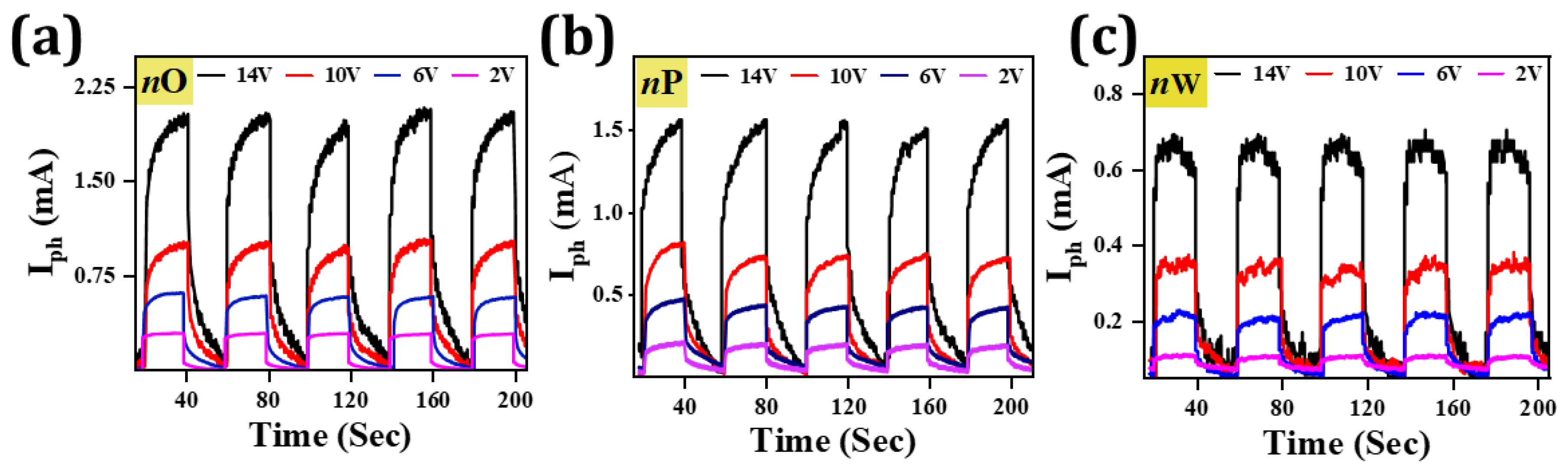
To evaluate the performance of the device, time-correlated transient photo response (I−T) measurements were carried out, as seen in
Figure 6. The photoresponse measurements were performed in such a way that the fabricated UVPD’s active area was exposed to a 325 nm UV laser with an optical power of 225 µW for periodic illuminations of 20 Sec “ON” and “OFF” with a continuously applied bias voltage (2 V to 14 V). A higher applied bias resulted in a stronger electric field that produced more photo carriers, which raised the I
ph value [
22]. The I
ph values for the nO increased from 0.3 mA to 2.0 mA as the bias increased from 2 V to 14 V. Moreover, the remaining nP (0.2 mA to 1.5 mA) and nW (0.1 mA to 0.7 mA) followed a similar trend with increasing bias. The I
ph value for the nO was much greater than the nP and nW. Further, the response (rise/decay) time of the developed detectors was assessed by fitting a single pulse (shown in
Figure S2, SI) of the experimentally acquired I−T at a fixed bias voltage of 2 V using the following equations [
23]:
where I
0 is the highest saturation I
ph value at a fixed time t, and the term t
r (t
d) stands for rise (decay) time, which is determined as the I
ph time to go from 10% to 90% of its peak value (called the rise time) and its time to go from 90% to 10% of its peak value (called the decay time). According to the outcome, the estimated t
r and t
d from the I−T acquired for nO were found to be the fastest (t
r = 1.1 s, t
d = 2.3 s) in comparison to the acquired signals for nP (t
r = 2.4 s, t
d = 3.9 s) and nW (t
r = 3.3 s, t
d = 3.9 s). The obtained result exhibited that all the fabricated UVPDs delivered a slow rise and decay time, which are attributed to the presence of deep and surface defect states in the semiconducting materials used to fabricate UVPDs [
24]. Conclusively, however, the observation revealed that for nO, the switching speed of the fabricated sensor was significantly less than others (nP and nW), i.e., nO < nP < nW.
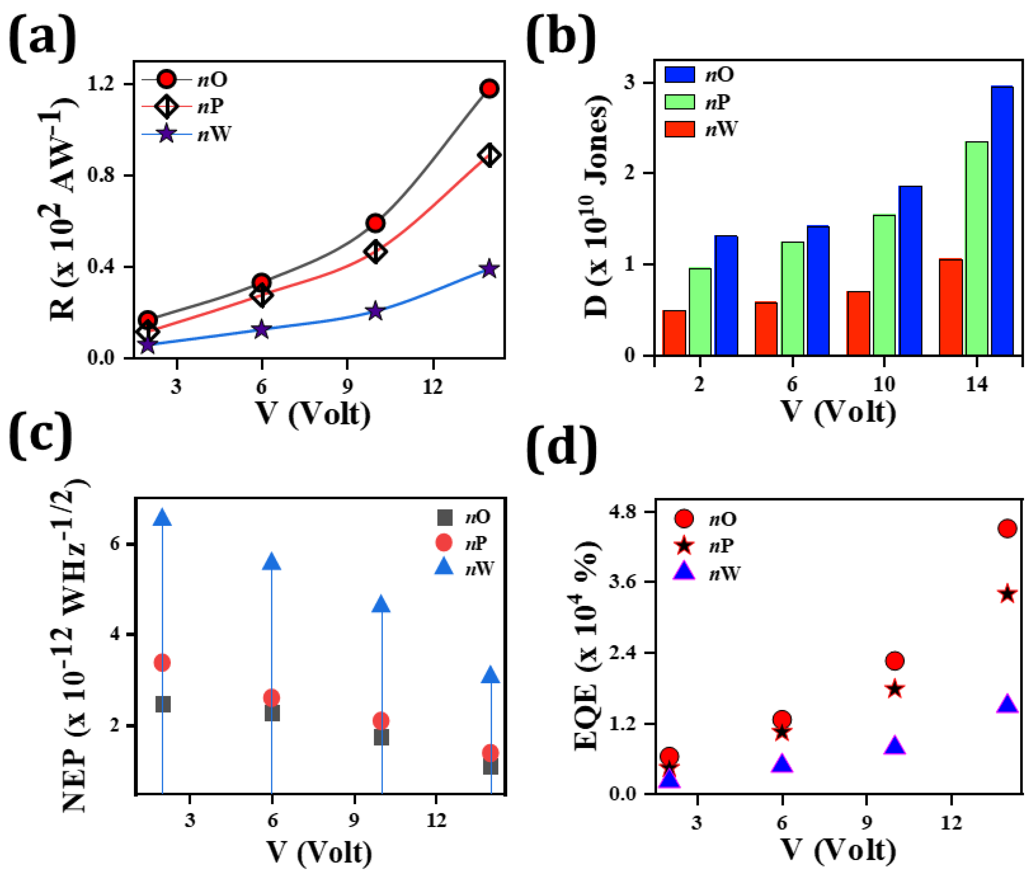
Further, the following equations were used to determine the key performance parameters of the fabricated PD, including responsivity (R), external quantum efficiency (EQE), noise equivalent power (NEP), and detectivity (D) [
25]:
where
Pd, Ao, c, h, and
e are their usual meanings. The
R values were calculated as 17 AW
−1, 11 AW
−1, and 5 AW
−1 for nO, nP, and nW, respectively, at a2 V applied bias which increased to 118 AW
−1 (nO), 88 AW
−1 (nP), and 38 AW
−1 (nW) under the 14 V applied bias, as depicted in
Figure 7a. In accordance with the investigation, the R-value for the nO-based device is ~34% and ~210% higher than the nP- and nW-based devices.
Additionally, the D value exhibited the same behavior as R and gained its maximum value at the 14 V bias under 225 µW ultraviolet light illumination, as shown in
Figure 7b. The highest D value was found to be 3.0 × 10
10 Jones, 2.3 × 10
10 Jones, and 1.0 × 10
10 Jones for the nO, nP, and nW, respectively.
Figure 7c displays the NEP of the fabricated devices where the value of NEP decreases with the increased bias. The lowest calculated value of NEP for nO at the 14 V bias was found to be 1.0 × 10
−12 WHz
−1/2, which was less than 1.4 × 10
−12 WHz
−1/2, and 3.0 × 10
−12 WHz
−1/2 for nP and nW. Furthermore, EQE values of the fabricated device were determined as a function of external bias, as shown in
Figure 7d. Similar to R, the EQE value was enhanced with external bias due to the augmentation in I
ph. The EQE of the PD reached the maximum value for nO under a 14 V external bias, 4.5 × 10
4%, and similarly, for nP and nW, it attained a value of 3.4 × 10
4% and 1.5 × 10
4%, respectively. In a standard PD, the EQE is 100%, indicating that a single photon produced a charge carrier that had undoubtedly contributed to the current conduction. A high value of EQE (>100%) indicates the existence of a photoconductive gain higher than unity [
16]. Finally, for better comparison, all the optimized performance parameters for all the heterostructures are displayed in
Table 2.


