Article

Effect of Carrier Gas Flow Rates on the Structural and Optical Properties of ZnO Films Deposited Using an Aerosol Deposition Technique

1
School of Materials and Mineral Resources Engineering, Engineering Campus, Universiti Sains Malaysia, Nibong Tebal 14300, Penang, Malaysia
2
Department of Physics, University of East Yangon, Thanlyin 11292, Myanmar
3
Institute of Liberal Arts & Sciences, Toyohashi University of Technology, 1-1 Hibarigaoka, Tempaku-cho, Toyohashi 441-8580, Japan
4
Department of Electrical and Electronic Information Engineering, Toyohashi University of Technology, 1-1 Hibarigaoka, Tempaku-cho, Toyohashi 441-8580, Japan
*
Author to whom correspondence should be addressed.
Electron. Mater. 2022, 3(4), 332-343; https://doi.org/10.3390/electronicmat3040027
Submission received: 16 September 2022 / Revised: 18 October 2022 / Accepted: 24 October 2022 / Published: 31 October 2022
(This article belongs to the Special Issue Feature Papers of Electronic Materials II)

Abstract

:
Aerosol deposition (AD) is a simple, dry raw-powder deposition process in which the targeted film is formed by direct bombardment of accelerated starting powder onto the substrate surface at room temperature. Despite the increased interest in AD film formation, no work has been completed to systematically investigate the formation of dense zinc oxide (ZnO) films using the AD method and their optical properties. Therefore, this study was carried out to investigate the effect of AD gas flow rate on the formation of AD films and the optical properties of aerosol-deposited ZnO films. ZnO films with nanosized (<40 nm) crystallites were successfully deposited on FTO substrates at room temperature. A dense and uniform layer of aerosol-deposited ZnO films with a roughened surface was obtained without subsequent heat treatment. With the increase in the AD gas flow rate, the crystal size and the AD film’s thickness were reduced. The Raman spectroscopy verified that the thin film was of a ZnO wurtzite structure. The room temperature photoluminescence of the ZnO thin film produced strong visible emissions. The findings of this work demonstrated that AD can be an alternative technique for the rapid deposition of dense and thick ZnO films for optoelectronic applications.

1. Introduction

Zinc oxide (ZnO) is a wide-band-gap (3.3 eV) compound semiconductor with a large exciton binding energy (60 meV) at room temperature [1]. It possesses unique properties such as high electron mobility (200 cm2·V−1·s−1) [2] and high optical transmittance (>90% in the visible-light regime) [3], and it exhibits room temperature photoluminescence (RTPL) with near-band-edge emissions at ~380 nm [4]. These unique properties make ZnO a potential candidate for applications such as transparent electrodes in liquid-crystal displays [5], thin-film transistors [6], light-emitting diodes [7], and dye-sensitized solar cells [8]. In addition, owing to its no-inversion-symmetry lattice arrangement, ZnO exhibits a piezoelectric property that can be used in microsensors and micro-actuators [9].
The structural and optical properties of ZnO films deposited on substrates are influenced by the deposition method as well as the post-deposition treatment. ZnO film deposition can be achieved using either the solution or vapor-route approaches. Solution approaches such as sol-gel [10], spin coating [11], and dip coating [12] have been used to coat a large surface area, but multiple steps are required. Therefore, these processes are very time consuming and thus not practical for industrial applications. On the other hand, vapor-route approaches, such as chemical-vapor deposition [13], flame-transport synthesis [14], magnetron sputtering [15], atomic-layer deposition (AD) [16], spray pyrolysis [17], pulsed-laser deposition [18], and aerosol deposition [19], have provided rapid and higher-precision ZnO film formation with controlled optical properties [20]. Nevertheless, these processes require sophisticated and expensive equipment such as a reactor and vacuum system [21]. Most of these methods are performed at elevated temperatures [22], which entails a higher fabrication cost [23].
The deposition of ZnO films in a rapid manner, especially at room temperature, is a practical and more affordable precision-coating technology. AD is one of the film deposition methods that utilizes fine particles accelerated to high speeds, which are transported through a carrier gas and bombarded onto a targeted substrate to produce high-density oxide films.
Carrier gases such as nitrogen or argon are commonly used for AD methods. Akedo et al. reported that the AD methods are commercially used for coating processes that are important for semiconductor fabrication equipment and to form thin or thick dense films of ceramics with a scale of several hundreds of nm or less at room temperature [24]. Moreover, investigations of the anchor layer formation on different substrates have been undertaken, and the feasibility of applying AD to control film optical properties has been demonstrated [20]. Thus, the flow rate of a carrier gas can affect the structural and optical properties of the films. To date, no work on the structural and optical properties of ZnO films prepared by the AD method has been reported. In this study, the effect of the carrier gas flow rates on the morphologies, crystallinity, and optical properties of ZnO films prepared using the AD process were systematically investigated. The findings from this work are beneficial for the development of a rapid deposition process to produce dense and thick ZnO films for optoelectronic applications.

2. Methodology

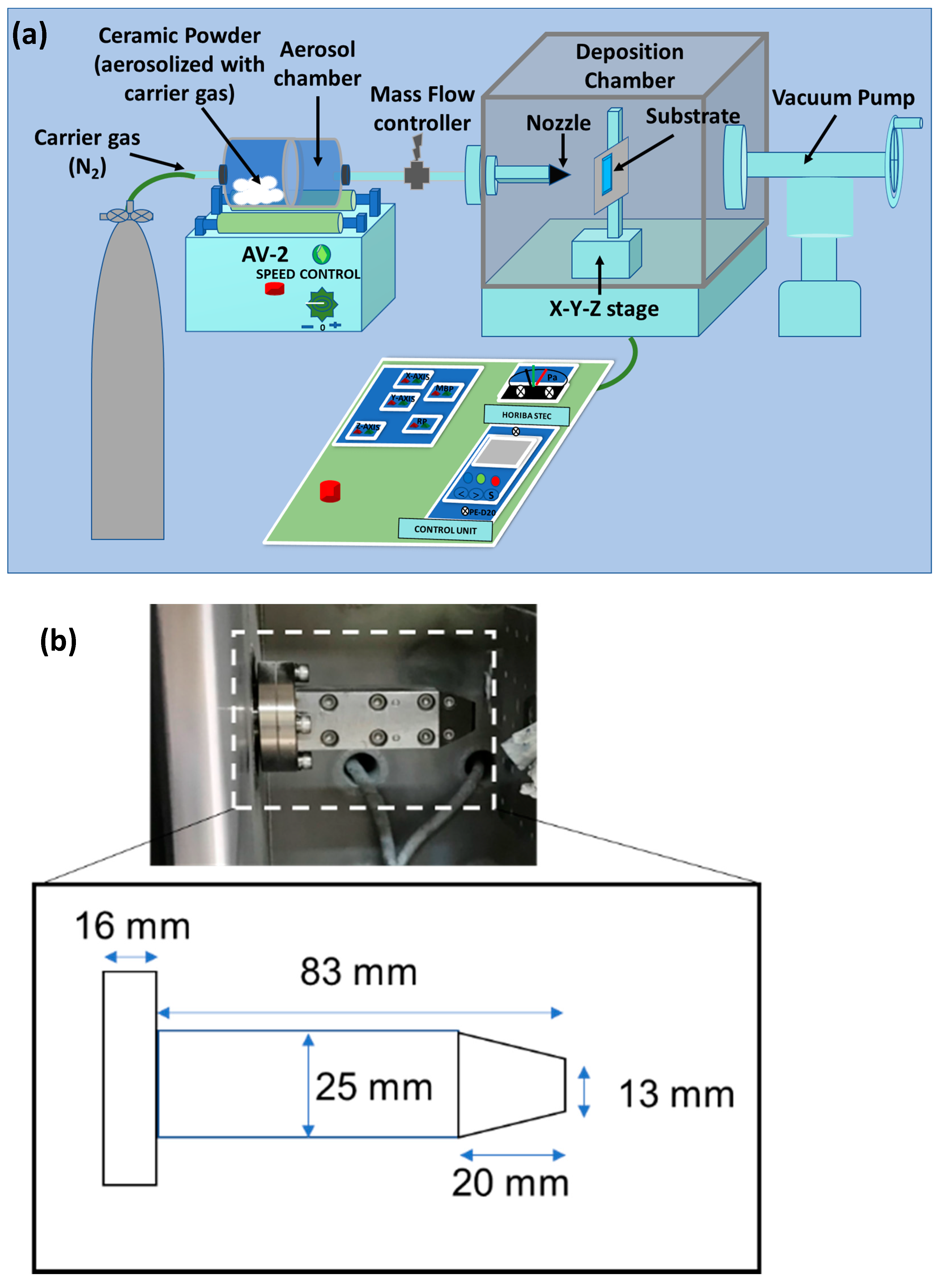
2.1. AD of ZnO Films

A schematic illustration of the AD equipment is shown in Figure 1a. The geometry of the nozzle used in AD is displayed in Figure 1b. The diameter and length of the nozzle are 25 mm and 83 mm, respectively. In a typical deposition process, 5 g of commercial ZnO (<100 nm, Sigma Aldrich, St. Louis, MO, USA) is used as starting powder. In this case, the powder was dried for 4 days at 100 °C to minimize powder aggregation by removing the residual moisture. Nitrogen gas with a purity of 99% was used as the carrier gas to carry and accelerate the ZnO powder toward the fluorine-doped tin-oxide (FTO) conductive glass substrate (20 × 30 mm2, 1.6 mm (t), Nippon Sheet Glass-FTN 1.6, Osaka, Japan) for the deposition process. The flow rates of the carrier gas (for acceleration of the ZnO powder) were varied at 30, 40, and 50 L/min. The scanning speed was kept at 3 mm/s. The pressure in the aerosol chamber was 20 Pa before aerosol deposition, and it was increased up to 150 Pa during aerosol deposition.
After AD was deposited on the substrates, the obtained samples were labelled as AD/Z-1, AD/Z-2, and AD/Z-3 for the carrier gas flow rates of 30, 40, and 50 L/min, respectively. During deposition, the pressure of the aerosol chamber was maintained at 20 Pa. The deposition time of each thin film was kept at 4 min and 15 s. The ZnO powder with high kinetic energy collided with the surface of the FTO-coated glass substrates, resulting in the formation of ZnO films via room temperature impact consolidation (RTIC). The area of the deposited film was 10 mm × 20 mm. The film thickness was adjustable by the number of deposited layers, while the other parameters were kept constant. After deposition, the ZnO films were dried at room temperature. The deposition parameters in the AD process are listed in Table 1.

2.2. Characterizations of AD ZnO Films

The crystal phase and diffraction planes of the ZnO powders and ZnO films were characterized using X-ray diffractometry (XRD, Rigaku RINT 2500) with Cu-Kα radiation (λ = 1.54059 Å). The microstructures of the raw powder and deposition films were observed using scanning electron microscopy (SEM, HITACHI, S-4800) at an acceleration voltage of 40 kV. The average film thickness from the cross-sectional view of the field-emission SEM (FESEM) images was calculated using Image J software. The optical properties of the ZnO films were analyzed using a UV-visible (UV-Vis) near-infrared spectrophotometer (V-670, JASCO Corporation; scanning range: 350–700 nm), a Raman spectroscope (NRS-3100, JASCO Corporation), and an RTPL spectroscope (KIMMON KOHA, Tokyo, Japan; excitation wavelength = 325 nm).

3. Results and Discussion

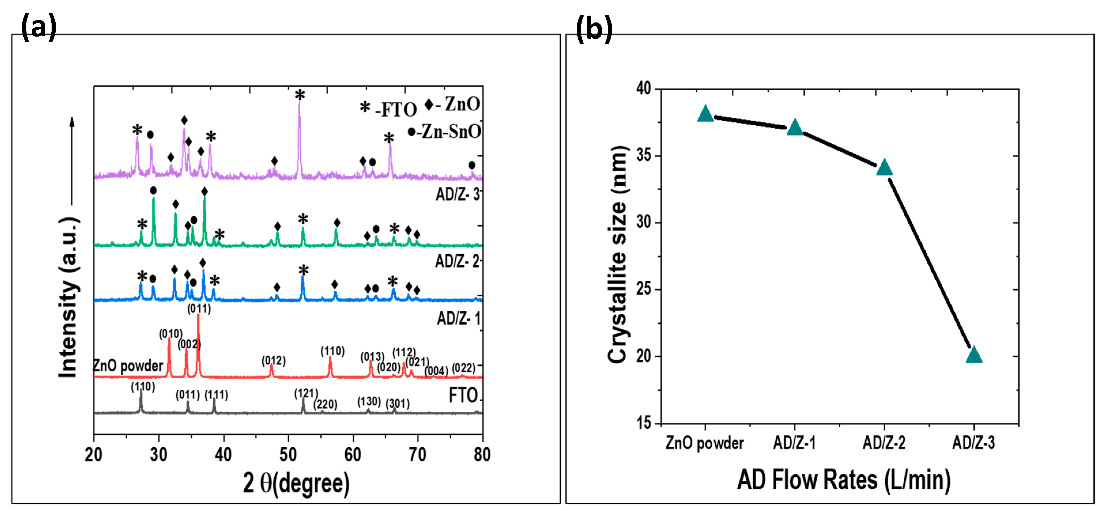
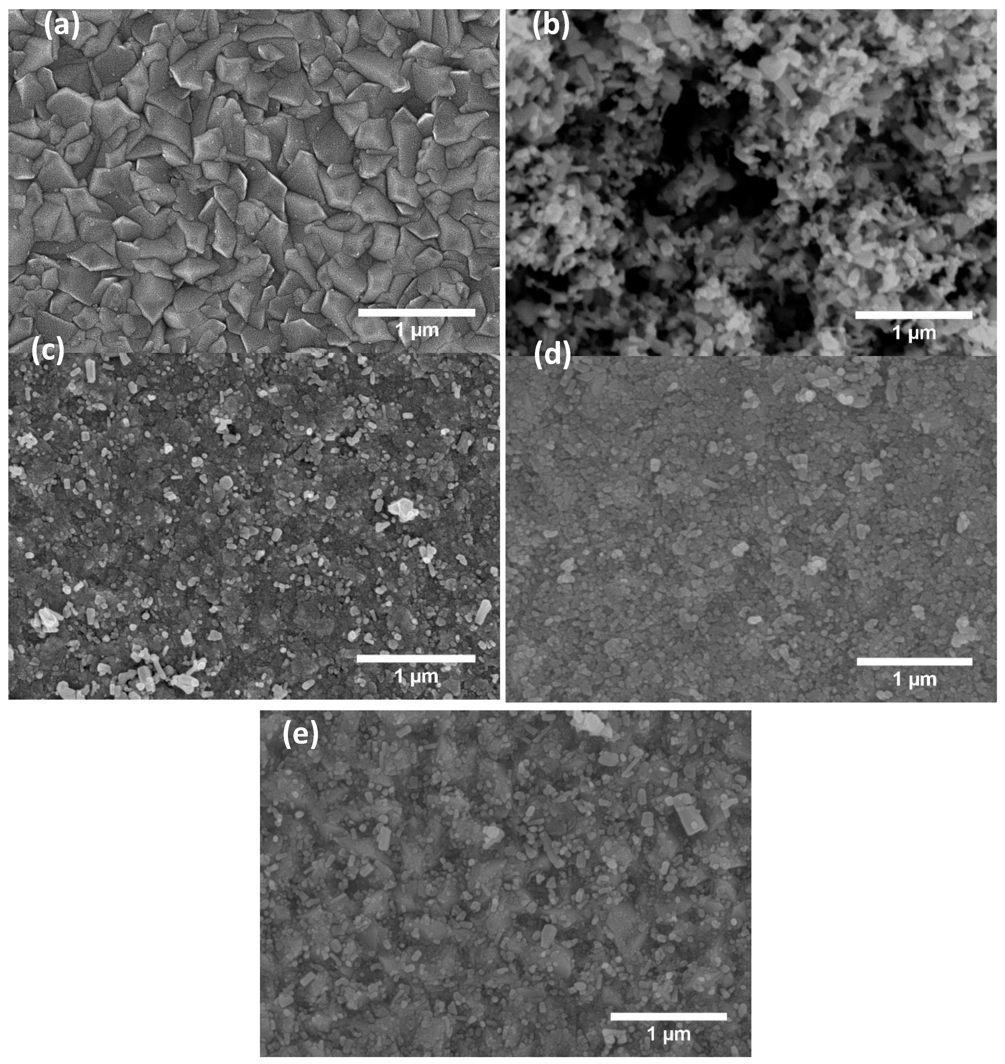
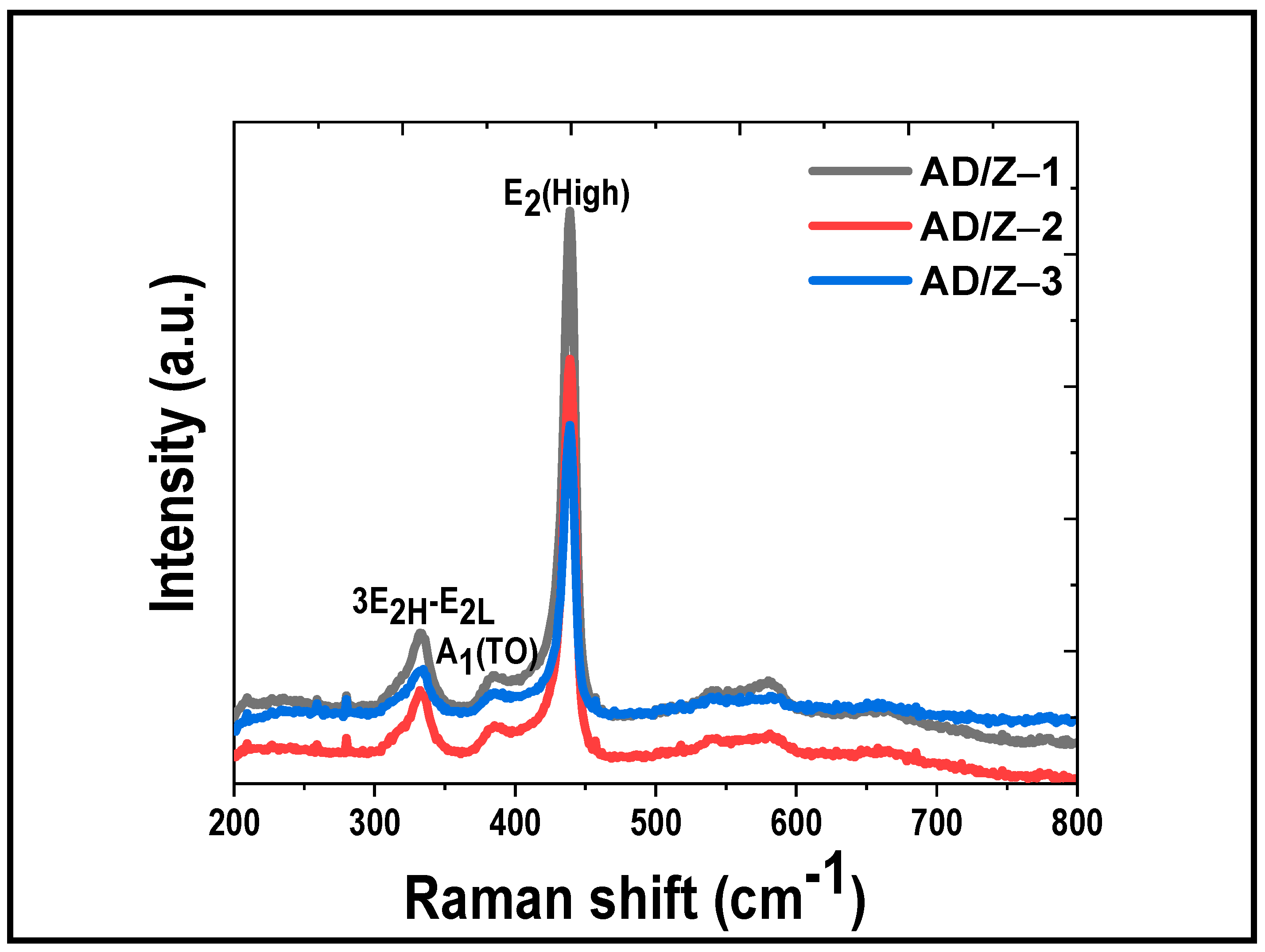
3.1. Structure and Morphology of the ZnO Films Deposited Using the AD Process

Dense films were obtained using the AD method at room temperature. The XRD patterns of the films for AD/Z-1, AD/Z-2, and AD/Z-3, prepared at the different flow rates of 30, 40, and 50 L/min, respectively, are shown in Figure 2a. The Bragg diffractions at 26.49°, 33.62°, 37.68°, 51.49°, 54.29°, 61.49°, and 65.51° correspond to the (110), (011), (020), (121), (220), (130), and (031) planes of tin (IV) oxide, respectively. The diffraction peaks of the tin (IV) oxide originated from the FTO-coated glass substrates (JCPDF-98-006-3707). The XRD peaks at diffraction angles of 31.55°, 34.20°, 36.04°, 47.33°, 56.39°, 62.67°, 66.19°, 67.76°, 68.90°, 72.39°, and 76.78°, respectively, are assignable to the (010), (002), (011), (012), (110), (013), (020), (112), (021), (004), and (022) planes of the ZnO hexagonal wurtzite structure (JCPDS-96-901-1663) from the ZnO raw powder. All diffraction peaks assignable to the hexagonal wurtzite structure of the ZnO (JCPDF-96-900-8878) were identified in all films produced by the AD process. A slight shift of the diffraction peaks for ADZ-2 and ADZ-3 to a larger 2θ was observed. This result is explainable. A higher nitrogen gas flow rate generated a higher impact on the ZnO thin films. As a result, the ZnO thin films produced were under compressive stress. Thus, the thin films have a smaller d spacing and a larger 2θ.
The crystallite size of the AD/ZnO films was estimated using the Debye–Scherrer formula, i.e., crystallite size, d = Kλ/β cos θ, where K is a constant (0.9), λ is the X-ray wavelength (1.5406 Å), and β is the broadening of the diffraction line measured at half of its maximum (FWHM) intensity (rad). The average crystal size of the ZnO powder was 38 nm. After deposition, the average crystal size of the ZnO films slightly decreased to 37, 34, and 20 nm for AD/Z-1, AD/Z-2, and AD/Z-3, respectively. This result indicated that the crystallite size of the ZnO films decreased with higher AD flow rates, as shown in Figure 2b. The results suggest that the ZnO powders were mechanically crushed and broken down into smaller crystallites by collision during the deposition process [25]. At higher flow rates, the higher kinetic energy of the ZnO powder led to stronger collision impacts and the fragmentation of the particles. Therefore, a smaller ZnO crystallite size was obtained.

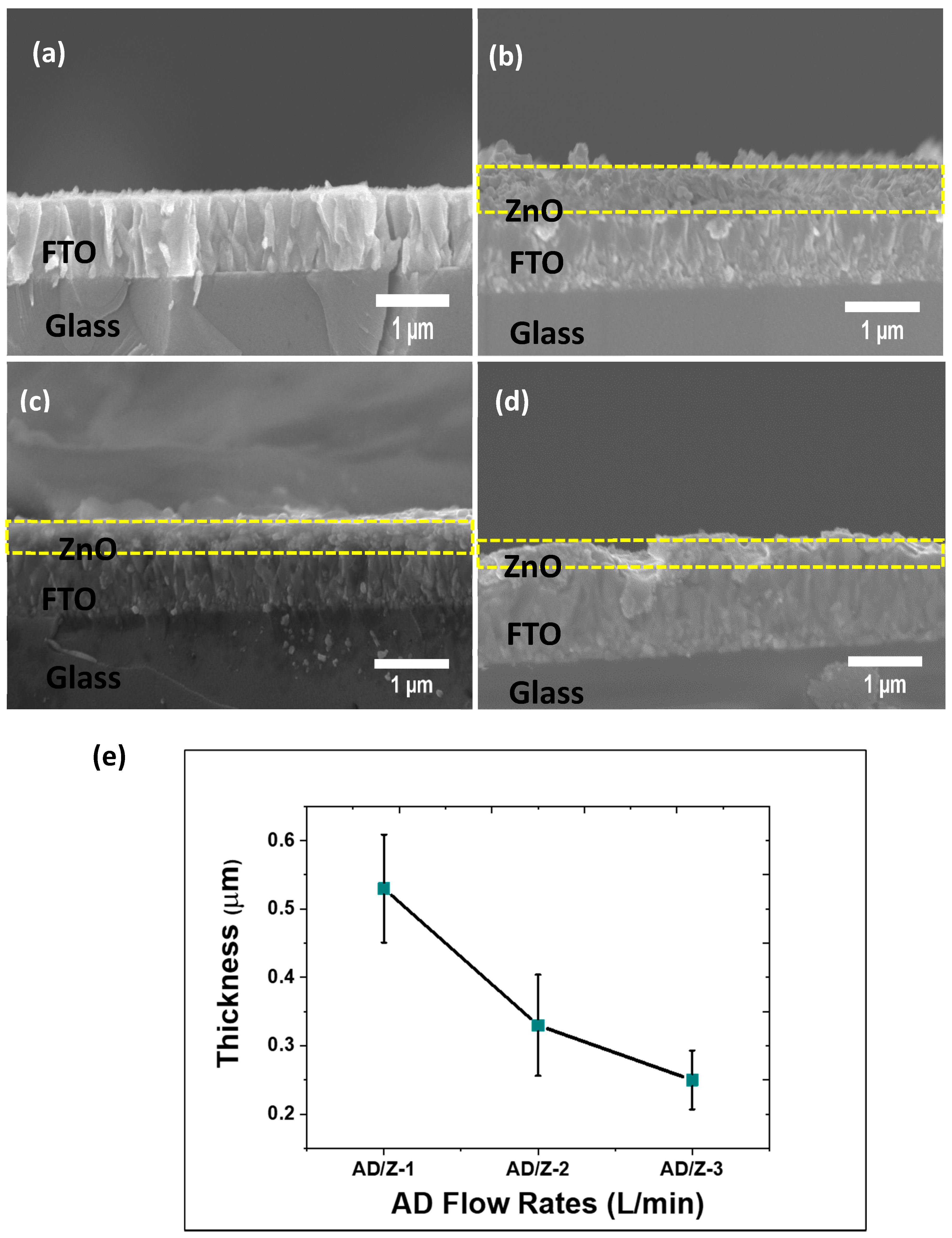
3.2. Morphologies and Thickness of the ZnO Films Deposited Using the AD Process

The advantage of the AD method is that dense ZnO films can be formed at room temperature using crystallized ZnO raw powder via the room temperature impact consolidation (RTIC) mechanism [26]. Figure 3 shows the FESEM images of the (a) bare FTO, (b) raw ZnO powder, (c) AD/Z-1, (d) AD/Z-2, and (e) AD/Z-3. Rough AD/ZnO film surfaces were obtained when an AD flow rate of 30 L/min was used, as shown in Figure 3c.
At a higher AD flow rate of 40 L/min, a higher acceleration of the ZnO powder generated higher kinetic energy, resulting in stronger collisions with the substrate and forming fine particle fractures, as shown in Figure 3d. Further increments of the AD flow rate resulted in surface etching and removal of the deposited film, similar to the sand-blasting effect [27], as illustrated in Figure 3e. As a result, the ADZ-3 film density was assumed to increase by undergoing fast deformation through becoming a finer powder.
The film thickness was influenced by the kinetic energy possessed by the ZnO powder prior to collision with the substrate, as well as the aggregation of the ZnO powder [28]. Figure 4a–d shows the cross-sectional view of the samples. The average thickness of the FTO was 0.66 µm. The average thickness of the ZnO thin films was 0.53, 0.33, and 0.25 µm for the AD/Z-1, AD/Z-2, and AD/Z-3 films, respectively. The thickness of the AD/ZnO films decreased with higher AD flow rates, as shown in Figure 4e. As the AD deposition parameters remained constant, the change in the film thickness were likely dependent on the powder concentration [28]. At low AD flow rates, most of the ZnO powders were bound in small and soft agglomerates that could be much more easily sprayed. Therefore, a thick and smooth ZnO film with and homogeneous surface would form on the FTO substrate. In contrast, a higher AD flow rate produced denser films because of the higher impact energy. The impact from the ZnO powder accelerated to a higher energy could dislodge or break the formed ZnO film, leading to a scattering of the particles away from the deposited films [29]. This result caused the decrease in the AD film thickness. Moreover, higher AD rates caused deformation of the substrate, which resulted in a roughened surface of the AD/ZnO films, as shown in Figure 4c,d.

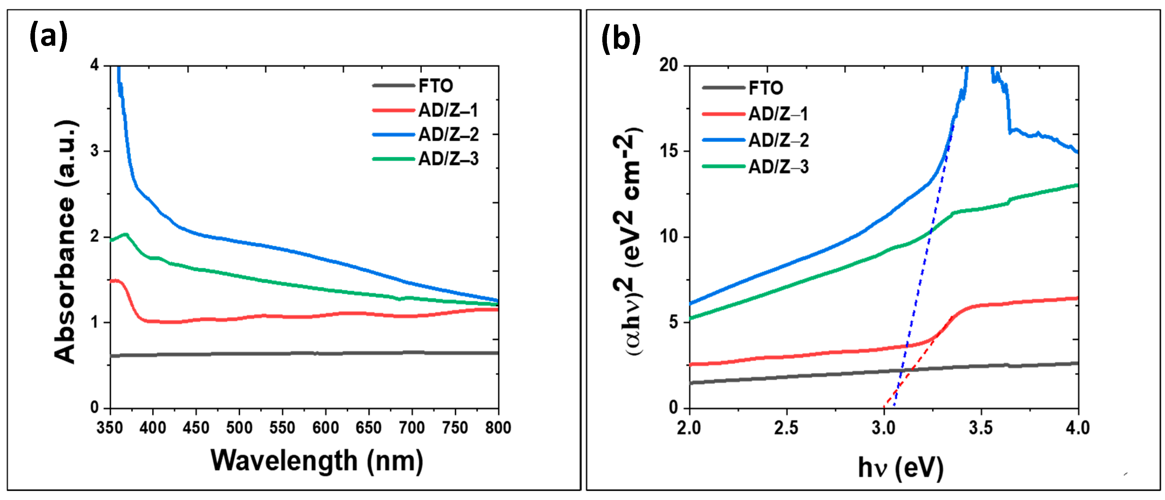
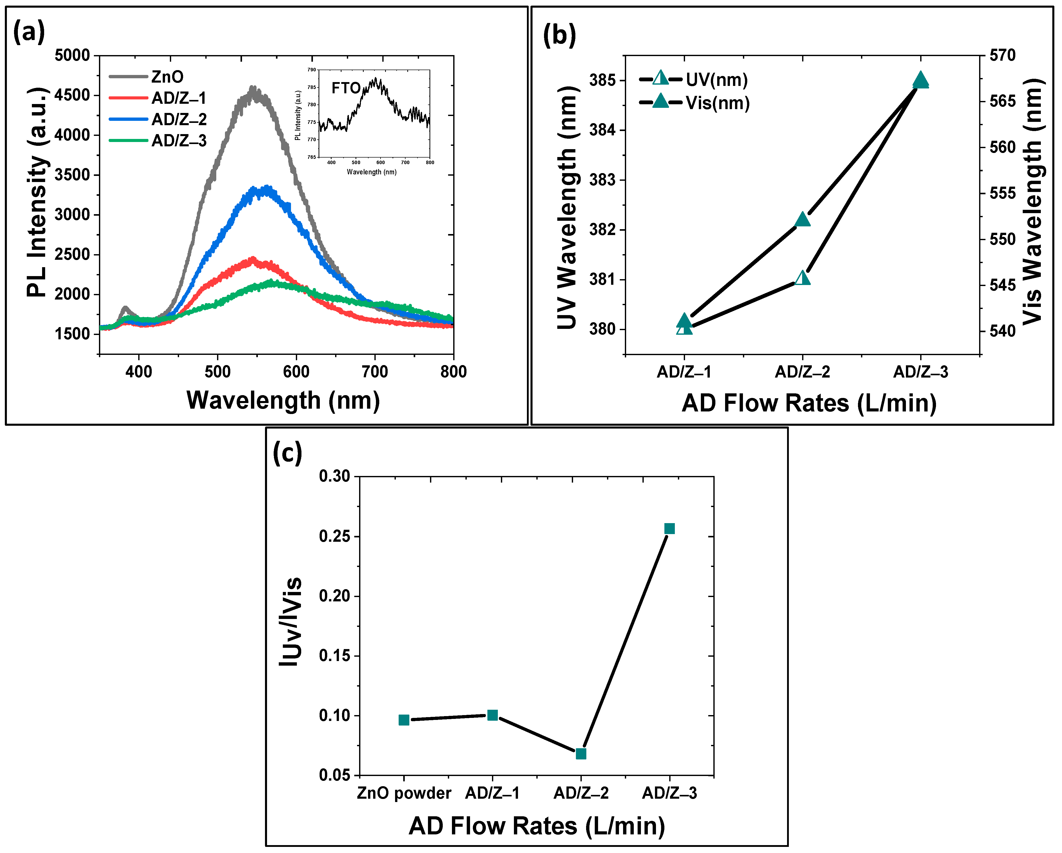
3.3. Optical Properties of the ZnO Films Deposited Using the AD Process

The optical properties of the ZnO films were analyzed and compared. Figure 5a shows the UV–Vis spectra of the ZnO films obtained using different flow rates. The results indicated that the optical properties of the AD/ZnO films varied with different AD flow rates. All ZnO films exhibited a typical UV absorbance at wavelengths of less than 400 nm. The ZnO film obtained at a flow rate of 30 L/min exhibited an absorption peak at approximately 360 nm. For the AD flow rates of 40 and 50 L/min, the UV absorption peaks were observed at 379 nm.
A Tauc’s plot was used to estimate the optical band-gap energy using the following formula: α E = B ( E E g   ) m   [30]. Here, B is a parameter that is independent of the photon energy (E), E g is the optical band-gap energy, and m = 1/2 represents the direct transition of the ZnO films. The estimated optical bandgaps were 2.99 and 3.02 eV for the ZnO films prepared using gas flow rates of 30 and 50 L/min, respectively. The bandgap of the ZnO film deposited using 40 L/min could not be determined due to the non-prominent slope, as shown in Figure 5b.
The room temperature Raman measurement of the ZnO films is shown in Figure 6. Two specific bands that corresponded to the 3E2HE2L frequency branch and E2 (high) optical modes at approximately 332 and 437 cm−1, respectively, were observed. Each active vibration mode corresponded to a band in the Raman spectra, and their intensity depended on the scattering cross-section of these modes. The E2 (high and low) and A1 transverse optical-phonon (TO) modes occurred when the irradiation was perpendicular to the c axis of the ZnO film [31]. The peak at 331 cm−1 (3E2HE2L) was the second-order Raman band that originated from the zone-boundary phonons associated with the vibration of the Zn sublattice [32].
The most intense and narrow peak at 437 cm−1 came from the first-order Raman scattering due to the E2 phonons of the ZnO, which exhibited the typical characteristic of a wurtzite lattice [33]. The intensity of the E2(H) band decreased with a higher flow rate due to the poorer crystallinity that resulted from the fragmentation of the ZnO crystal because of the higher collision impact during the RTIC. From the results, the AD/Z-1 film was demonstrated to be the best film, with a good crystallite structure. In addition, the peak at 382 cm−1 was attributed to the A1 (TO) mode in the spectra due to the ZnO’s anisotropic nature [34].
An RTPL analysis was performed to investigate the optical property and crystal quality of the FTO glass substrate, ZnO powder (commercial), and ZnO thin films prepared at the various AD flow rates. As shown in Figure 7a, all ZnO samples exhibited a UV emission (near-band-edge transition, NBE) at 383 nm and a broad visible light emission (defect-related emission, also known as deep-level emission (DLE)) at 540–570 nm in the green–yellow region. The NBE emission band was related to the near-band-edge transition of the free excitons [35]. The DLEs were centered at 544-, 554-, and 567-nm for the AD/Z-1, AD/Z-2, and AD/Z-3 thin films, respectively. The green emission may have originated from the transitions between the electrons in the conduction band to the oxygen-vacancy-related defect energy level in the bandgap, whereas the yellow emission at 567 nm suggests the presence of singly negative-charged interstitial oxygen-ion defects (Oi) [36]. It is worth mentioning that the green-yellow emission did not originate from the FTO glass substrate. As shown in the inset of Figure 7a, the FTO glass substrate produced a very weak emission at 580 nm. The emission peak was different compared to the DLEs from the ZnO thin films.
The ZnO powder exhibited weak UV emissions at 383 nm and a strong visible light emission at 540–570 nm in the green–yellow region. This suggests that the ZnO powder contained a large amount of crystal defects. A similar observation was found for the ZnO thin films, i.e., producing weak UV emissions but strong visible light emissions. The IUV/IVis ratios for the ZnO thin films were generally low, i.e., 0.101, 0.068, and 0.257 for AD/Z-1, AD/Z-2, and AD/Z-3, respectively, as shown in Figure 7c. The results indicate that the number of defects in the ZnO thin films was approximately the same compared to their ZnO powder.
It is noted that bandgap of the ZnO films calculated from the NBE (383 nm) was ~3.24 eV. This bandgap (RTPL) is slightly larger than the bandgap estimated from the UV-visible absorbance of the Tauc plot, as shown in Figure 5. The slight deviation in the bandgaps could be due to the origin of the characterization signal and the model (Tauc plot) that were used in the estimation. The NBE in the RTPL originated from the relaxation of the optically excited electrons from the conduction band to the valence band. As a result, UV light was emitted from the ZnO films. The emitted UV light was captured by the spectrometer, which is known as NBE. The bandgap was directly converted from the NBE wavelength. Contrarily, the absorbance of UV light by the ZnO films was first measured by a UV-visible light spectrometer (the adsorbed light could cause optical excitation on the ZnO films in a subsequent stage). The bandgap of the ZnO films was indirectly estimated from the Tauc plot.

4. Conclusions

ZnO films have been successfully deposited on FTO substrates at room temperature using the AD method. The optical properties of the aerosol-deposited films were investigated as functions of the carrier gas flow rate, as this would alter the kinetic energy possessed by ZnO particles prior to collision with the substrates. The carrier gas flow rate was varied from 30 L/min to 40 L/min and 50 L/min, and ZnO films exhibiting dense and uniform-thicknesses with rough surfaces were obtained without any subsequent heat treatment. The results showed that the crystallite size decreased from 38 nm (powder) to 20 nm when a higher gas flow rate was used, implying a stronger collision upon impact with the substrate, causing more severe fracturing/breakage of the particles. Surface morphological observation revealed that rough and dense ZnO films were obtained. The thickness of the films was reduced from 1.2 µm to 0.91 µm when the gas flow rate was increased from 30 L/min to 50 L/min. The blasting effect at a higher flow rate caused surface roughening of the outer layer of the ZnO films. The optical characterization results indicated a reduction in the bandgap with higher gas flow rates, i.e., from 3.23 eV (30 L/min) to 3.14 eV (50 L/min), while the RTPL of the ZnO films exhibited both UV emissions at 383 nm and strong visible light (defect-related) emissions at 540–570 nm. The Raman analysis showed that the aerosol-deposited films contained ZnO with wurtzite crystallite structures. The findings from this study indicate the rapid formation of ZnO films by the AD method is feasible, and its further development to obtain ZnO films with the desired optical properties would be of use for optoelectronic applications.

Author Contributions

Conceptualization, M.Z.T. and W.K.T.; methodology, M.Z.T. and W.K.T.; formal analysis, M.Z.T. and S.-Y.P.; investigation, M.Z.T.; re-sources, W.K.T., G.K. and H.M.; writing—original draft preparation, M.Z.T.; writing—review and editing, W.K.T., H.M., G.K., A.M., K.A.B.Y. and S.-Y.P.; supervision, S.-Y.P. and A.M.; funding acquisition, S.-Y.P. and W.K.T. All authors have read and agreed to the published version of the manuscript.

Funding

This research was funded by AUN/SEED-Net grant number 304.PBAHAN.6050390/J135 and Japan Society for the Promotion of Science (JSPS) KAKENHI Grant Number 22H01790.

Data Availability Statement

The data will be provided if requested.

Acknowledgments

This work was also partially supported by the Kazuchika Okura Memorial Foundation. Hiroto Sekiguchi of the Toyohashi University of Technology (TUT) is acknowledged for performing the photoluminescence measurements.

Conflicts of Interest

The authors declare no conflict of interest.

References

  1. Pearton, S.; Norton, D.; Ip, K.; Heo, Y.; Steiner, T. RETRACTED: Recent progress in processing and properties of ZnO. Prog. Mater. Sci. 2005, 50, 293–340. [Google Scholar] [CrossRef]
  2. Hutson, A.R. Hall effect studies of doped zinc oxide single crystals. Phys. Rev. 1957, 108, 222. [Google Scholar] [CrossRef]
  3. Sahu, D.; Lin, S.-Y.; Huang, J.-L. ZnO/Ag/ZnO multilayer films for the application of a very low resistance transparent electrode. Appl. Surf. Sci. 2006, 252, 7509–7514. [Google Scholar] [CrossRef]
  4. Bagnall, D.; Chen, Y.; Shen, M.; Zhu, Z.; Goto, T.; Yao, T. RT excitonic stimulated emission from zinc oxide epilayers grown by plasma assisted MBE. In Nanoelectronics and Nanotechnology; University of Southampton: Iskandar Puteri, Malaysia, 1998. [Google Scholar]
  5. Shimizu, T.; Nakada, M.; Tsuda, H.; Akedo, J.; Nishi, K.; Ohashi, K. Optical Characteristics of a PZT Waveguide Fabricated Using Aerosol Deposition for Optical Modulators on LSI Chips. In Proceedings of the 2007 Sixteenth IEEE International Symposium on the Applications of Ferroelectrics, Nara, Japan, 27–31 May 2007; pp. 831–833. [Google Scholar]
  6. Hoffman, R.; Norris, B.J.; Wager, J. ZnO-based transparent thin-film transistors. Appl. Phys. Lett. 2003, 82, 733–735. [Google Scholar] [CrossRef]
  7. Trung, D.; Quang, N.; Tran, M.; Du, N.; Tu, N.; Hung, N.; Viet, D.X.; Anh, D.; Huy, P. Single-composition Al3+-singly doped ZnO phosphors for UV-pumped warm white light-emitting diode applications. Dalton Trans. 2021, 50, 9037–9050. [Google Scholar] [CrossRef]
  8. Javed, A.H.; Shahzad, N.; Khan, M.A.; Ayub, M.; Iqbal, N.; Hassan, M.; Hussain, N.; Rameel, M.I.; Shahzad, M.I. Effect of ZnO nanostructures on the performance of dye sensitized solar cells. Sol. Energy 2021, 230, 492–500. [Google Scholar] [CrossRef]
  9. Zhang, Y.-H.; Wang, C.-N.; Gong, F.-L.; Chen, J.-L.; Xie, K.-F.; Zhang, H.-L.; Fang, S.-M. Ultra-sensitive triethylamine sensors based on oxygen vacancy-enriched ZnO/SnO2 micro-camellia. J. Mater. Chem. C 2021, 9, 6078–6086. [Google Scholar] [CrossRef]
  10. Pan, W.; Han, Y.; Wang, Z.; Gong, C.; Guo, J.; Lin, J.; Luo, Q.; Yang, S.; Ma, C.-Q. An efficiency of 14.29% and 13.08% for 1 cm2 and 4 cm2 flexible organic solar cells enabled by sol–gel ZnO and ZnO nanoparticle bilayer electron transporting layers. J. Mater. Chem. A 2021, 9, 16889–16897. [Google Scholar] [CrossRef]
  11. Shafi, M.A.; Bouich, A.; Fradi, K.; Guaita, J.M.; Khan, L.; Mari, B. Effect of deposition cycles on the properties of ZnO thin films deposited by spin coating method for CZTS-based solar cells. Optik 2022, 258, 168854. [Google Scholar] [CrossRef]
  12. Toe, M.Z.; Pung, S.-Y.; Yaacob, K.A.B.; Han, S.S. Effect of dip-coating cycles on the structural and performance of ZnO thin film-based DSSC. Arab. J. Sci. Eng. 2021, 46, 6741–6751. [Google Scholar] [CrossRef]
  13. Purica, M.; Budianu, E.; Rusu, E.; Danila, M.; Gavrila, R. Optical and structural investigation of ZnO thin films prepared by chemical vapor deposition (CVD). Thin Solid Films 2002, 403, 485–488. [Google Scholar] [CrossRef]
  14. Mishra, Y.K.; Kaps, S.; Schuchardt, A.; Paulowicz, I.; Jin, X.; Gedamu, D.; Freitag, S.; Claus, M.; Wille, S.; Kovalev, A. Fabrication of Macroscopically Flexible and Highly Porous 3D Semiconductor Networks from Interpenetrating Nanostructures by a Simple Flame Transport Approach. Part. Part. Syst. Charact. 2013, 30, 775–783. [Google Scholar] [CrossRef]
  15. Lee, J.B.; Kim, H.J.; Kim, S.G.; Hwang, C.S.; Hong, S.-H.; Shin, Y.H.; Lee, N.H. Deposition of ZnO thin films by magnetron sputtering for a film bulk acoustic resonator. Thin Solid Films 2003, 435, 179–185. [Google Scholar] [CrossRef]
  16. Pung, S.-Y.; Choy, K.-L.; Hou, X.; Shan, C. Preferential growth of ZnO thin films by the atomic layer deposition technique. Nanotechnology 2008, 19, 435609. [Google Scholar] [CrossRef] [PubMed]
  17. Andrade, E.; Miki-Yoshida, M. Growth, structure and optical characterization of high quality ZnO thin films obtained by spray pyrolysis. Thin Solid Films 1999, 350, 192–202. [Google Scholar]
  18. Shukla, R.; Srivastava, A.; Srivastava, A.; Dubey, K. Growth of transparent conducting nanocrystalline Al doped ZnO thin films by pulsed laser deposition. J. Cryst. 2006, 294, 427–431. [Google Scholar] [CrossRef]
  19. Chen, S.; Wilson, R.M.; Binions, R. Synthesis of highly surface-textured ZnO thin films by aerosol assisted chemical vapour deposition. J. Mater. Chem. A 2015, 3, 5794–5797. [Google Scholar] [CrossRef] [Green Version]
  20. Tan, W.K.; Shigeta, Y.; Yokoi, A.; Kawamura, G.; Matsuda, A.; Muto, H. Investigation of the anchor layer formation on different substrates and its feasibility for optical properties control by aerosol deposition. Appl. Surf. Sci. 2019, 483, 212–218. [Google Scholar] [CrossRef]
  21. Ehsan, M.A.; Shah, S.S.; Basha, S.I.; Hakeem, A.S.; Aziz, M.A. Recent Advances in Processing and Applications of Heterobimetallic Oxide Thin Films by Aerosol-assisted Chemical Vapor Deposition. Chem. Rec. 2021, 22, e202100278. [Google Scholar] [CrossRef]
  22. Al Jarrah, R.M.; Kadhem, E.M.; Alkhayatt, A.H.O. Annealing and operating temperatures effect on spray-deposited nanocrystalline ZnO thin-film gas sensor. Appl. Phys. A 2022, 128, 527. [Google Scholar] [CrossRef]
  23. Abd-Alghafour, N.; Kadhim, I.H.; Naeem, G.A. UV detector characteristics of ZnO thin film deposited on Corning glass substrates using low-cost fabrication method. J. Mater. Sci. Mater. Electron. 2021, 1–12. [Google Scholar] [CrossRef]
  24. Akedo, J. Room temperature impact consolidation and application to ceramic coatings: Aerosol deposition method. J. Ceram. Soc. Jpn. 2020, 128, 101–116. [Google Scholar] [CrossRef] [Green Version]
  25. Imanaka, Y.; Amada, H.; Kumasaka, F.; Takahashi, N.; Yamasaki, T.; Ohfuchi, M.; Kaneta, C. Nanoparticulated Dense and Stress-F ree Ceramic Thick Film for Material Integration. Adv. Eng. Mater. 2013, 15, 1129–1135. [Google Scholar] [CrossRef]
  26. Akedo, J. Aerosol Deposition (AD) Process: The Basic and Applications—Novel Ceramic Coating Technology with Room Temperature Impact Consolidation (RTIC); CMC Publishing Co., Ltd.: Tokyo, Japan, 2008. [Google Scholar]
  27. Abbas, M.; Mehran, M.T.; Moon, M.-W.; Byun, J.Y.; Kim, S.H. Wettability Control of Modified Stainless Steel Surfaces for Oxide Catalyst Carrier Slurry Coating. J. Ind. Eng. Chem. 2020, 91, 330–339. [Google Scholar] [CrossRef]
  28. Hanft, D.; Glosse, P.; Denneler, S.; Berthold, T.; Oomen, M.; Kauffmann-Weiss, S.; Weis, F.; Häßler, W.; Holzapfel, B.; Moos, R. The aerosol deposition method: A modified aerosol generation unit to improve coating quality. Materials 2018, 11, 1572. [Google Scholar] [CrossRef] [PubMed] [Green Version]
  29. Abe, H.; Miyamoto, Y.; Umetsu, M.; Uchikoshi, T.; Okubo, T.; Naito, M.; Hotta, Y.; Kasuga, T.; Suda, A.; Mori, H. Nanoparticle Technology Handbook; Elsevier: London, UK, 2008; pp. 177–265. [Google Scholar]
  30. Debanath, M.; Karmakar, S. Study of blueshift of optical band gap in zinc oxide (ZnO) nanoparticles prepared by low-temperature wet chemical method. Mater. Lett. 2013, 111, 116–119. [Google Scholar] [CrossRef]
  31. Das, D.; Mondal, P. Photoluminescence phenomena prevailing in c-axis oriented intrinsic ZnO thin films prepared by RF magnetron sputtering. Rsc Adv. 2014, 4, 35735–35743. [Google Scholar] [CrossRef]
  32. Fedorov, A.; Baranov, A.; Inoue, K. Exciton-phonon coupling in semiconductor quantum dots: Resonant Raman scattering. Phys. Rev. B 1997, 56, 7491. [Google Scholar] [CrossRef]
  33. Chen, S.; Liu, Y.; Lu, Y.; Zhang, J.; Shen, D.; Fan, X. Photoluminescence and Raman behaviors of ZnO nanostructures with different morphologies. J. Cryst. Growth 2006, 289, 55–58. [Google Scholar] [CrossRef]
  34. Zhang, R.; Yin, P.-G.; Wang, N.; Guo, L. Photoluminescence and Raman scattering of ZnO nanorods. Solid State Sci. 2009, 11, 865–869. [Google Scholar] [CrossRef]
  35. Spanhel, L.; Anderson, M.A. Semiconductor clusters in the sol-gel process: Quantized aggregation, gelation, and crystal growth in concentrated zinc oxide colloids. J. Am. Chem. Soc. 1991, 113, 2826–2833. [Google Scholar] [CrossRef]
  36. Wu, X.; Siu, G.; Fu, C.; Ong, H. Photoluminescence and cathodoluminescence studies of stoichiometric and oxygen-deficient ZnO films. Appl. Phys. Lett. 2001, 78, 2285–2287. [Google Scholar] [CrossRef]
Figure 1. (a) Schematic diagram of the AD process, and (b) the geometry of the nozzle.
Electronicmat 03 00027 g001
Figure 2. (a) XRD pattern, and (b) crystallite size that varied with the AD flow rates.
Electronicmat 03 00027 g002
Figure 3. FESEM images of (a) bare FTO, (b) ZnO powder, (c) AD/Z-1, (d) AD/Z-2, and (e) AD/Z-3 on the FTO substrate at different AD flow rates.
Electronicmat 03 00027 g003
Figure 4. FESEM cross-sectional view of (a) bare FTO, (b) AD/Z-1, (c) AD/Z-2, (d) AD/Z-3, and (e) the thickness variations in the ZnO films deposited by various AD rates.
Electronicmat 03 00027 g004
Figure 5. (a) UV–visible absorption spectra, and (b) Tauc plot of the ZnO films deposited using different AD flow rates.
Electronicmat 03 00027 g005
Figure 6. Raman spectra of the ZnO films deposited using the AD process.
Electronicmat 03 00027 g006
Figure 7. (a) RTPL spectra. (b) Maximum peak of the UV and visible emissions. (c) Ratio of the UV–Vis emissions of the AD/ZnO films deposited at different AD flow rates.
Electronicmat 03 00027 g007
Table 1. Deposition parameters of the ZnO films using the AD process.
Deposition Parameters
Raw materialZnO (<100 nm) commercial powder
Carrier gas flow rate (L/min)30, 40, and 50
Deposition time (min)4 min 15 s per film
Carrier gasNitrogen
Pressure (Pa)20
SubstrateFTO (20 mm × 30 mm, thickness: 1.6 mm)
Working distance (mm)10
Deposition temperatureRoom temperature
Publisher’s Note: MDPI stays neutral with regard to jurisdictional claims in published maps and institutional affiliations.

