Article

Detection, Characterization and Modeling of Localized Defects and Thermal Breakdown in Photovoltaic Panels from Thermal Images and IV Curves

1
Faculty of Engineering of Bilbao, University of the Basque Country (UPV/EHU), 48940 Leioa, Spain
2
ESTIA Institute of Technology, University Bordeaux, F-64210 Bidart, France
*
Author to whom correspondence should be addressed.
Electron. Mater. 2022, 3(2), 154-172; https://doi.org/10.3390/electronicmat3020014
Submission received: 30 November 2021 / Revised: 4 March 2022 / Accepted: 23 March 2022 / Published: 1 April 2022
(This article belongs to the Special Issue Feature Papers of Electronic Materials)

Abstract

:
In this work, a defective commercial module with a rounded IV characteristic is analyzed in detail to identify the sources of its malfunction. The analysis of the module includes thermography images taken under diverse conditions, the IV response of the module obtained without any shadow, and shadowing one cell at a time, as recommended by the IEC 61215 Standard. Additionally, a direct measurement of the IV characteristic and resistance of single cells in the panel has been conducted to verify the isolation between the p and n areas. In parallel, theoretical cell and module behaviors are presented. In this frame, simulations show how cell mismatch can be the explanation to the rounded IV output of the solar panel under study. From the thermal images of the module, several localized hot spots related to failing cells have been revealed. During the present study, thermal breakdown is seen before avalanche breakdown in one of the cells, evidencing a hot spot. Not many papers have dealt with this problem, whereas we believe it is important to analyze the relationship between thermal breakdown and hot spotting in order to prevent it in the future, since hot spots are the main defects related to degradation of modern modules.

1. Introduction

In the search for an energy system based on renewable sources, PV conversion turns out to be of utmost importance. The vast majority of the current PV generation comes from silicon-based solar panels [1,2]. There is a justified interest both on their modeling—for generation prediction purposes [3,4,5]—and in their sorting—in order to reach high module reliability [6,7]. In this frame, different solutions have been proposed to detect and prevent failures in silicon PV systems [8,9], panels and cells [10].
The panels are modeled using the standard models for cell characterization. Some articles describe the characterization of this kind of panel by the cell’s one or two-diode circuit models [4,11,12,13], shown in Figure 1 and Figure 2, with several methods for the parameter extraction [14,15,16]. The current that can be extracted from the cell (ICELL) will be equal to the current photogenerated in the cell (IPH) minus the darkness or recombination current (IDARK). The darkness current includes the recombination in the diode and resistive losses associated with poor isolation (low parallel resistance, RP) and poor contact (high series resistance, RS). The difference between these two models is that the two-diode model separates the recombination current into two terms, represented by two diodes: one related to the recombination in the emitter (ID1) and the other to the recombination in the junction (ID2), allowing for greater accuracy. Equations (1) and (2) represent the ICELL expressions for the one- and two-diode models, respectively.
I CELL = I PH I DARK = I PH I 01 · exp ( ( V CELL + I CELL · R S ) n · V T ) G SH · ( V CELL + I CELL · R S )
I CELL = I PH I DARK = I PH I D 01 · exp ( ( V CELL + I CELL · R S ) V T ) I D 02 · exp ( ( V CELL + I CELL · R S ) 2 · V T ) G SH · ( V CELL + I CELL · R S )
A photovoltaic panel consists of some cell strings connected in series or in parallel. Each string is composed of a number of cells in series, which compels them to work at the same current point. A difference in the output characteristic of a cell would make it work at a different voltage point compared to the rest of the cells in its string, resulting in the fill-factor (FF) of the module being poorer than expected. Cells are measured and classified into groups of similar characteristics prior to module mounting, which could diminish but not completely avoid the scattering in the same module [17,18,19]. However, simple system aging can lead to considerable mismatch [18,20]. This is particularly true in multicrystalline silicon cells, where intragrain dislocations and impurity precipitates can lead to non-uniform current distribution and appearance of hot spots [21]. A correlation has also been observed between the micro cracks in the structure of the solar cells and the appearance of hot spots [22]. Severe hot spot cases can be detected by simple visual inspection, since they lead to browned cells and blisters in the rear of the module, which degrade the response of the entire panel. Cell damage impacts the IV output. In the IEA’s review of failures of photovoltaic modules, a table relates possible failures in photovoltaic panels with their output IV characteristic [23]. Long-term studies under real operating conditions and diverse climatologic environments have shown that module aging leads to degradation in performance and to power loss [24,25,26,27], mainly due to a strong decrease in the short circuit current, ISC [27].
Regarding the failure type, the studies with older modules show a low presence of hot spots, whereas hot spotting is the main degradation problem for every climatologic condition in modules installed since 2000 [28]. High scale production and the introduction of multicrystalline modules to the market is probably related to this fact, since in well-processed monocrystalline silicon cells, hot spots do not seem to be an issue [29].
Even if all the cells in a module were identical, the equal functioning of all the cells would not be guaranteed. There are different types of possible shadowing, some of which are unavoidable. Clouds, for instance, can generate areas with lower irradiance; this would generate an output IV curve with different maximum power points (MPP). Different configurations have been proposed and studied to blur the effect of these types of shadows [30,31]. Smaller and less diffuse shadows—due to a leaf or a bird dropping—can also occur. In this case, the IV curve of the shadowed cell shifts down in proportion to the shadowed area, blocking the current in the string to some extent. This pushes the illuminated cells close to becoming open circuits and the shadowed cell to negative voltages. The reversed cell is now consuming energy instead of generating it: its temperature will increase, eventually creating hot spots, which could permanently damage the cell [32]. This situation has been widely analyzed along with the other degradation phenomena that reduce output power [19,33,34]. A bypass diode connected in parallel to a cell can offer protection under partial shades or shunting, but, normally, diodes are not connected in parallel to each single cell, but to a string of cells connected in series, or a subpanel, which aims to keep manufacturing costs to a minimum. Recently, modifications using MOSFETs and IGBTs have been proposed as more efficient alternatives to prevent hot spots in modules [19,35,36,37].
The identification and prediction of failures in PV panels can be performed by several techniques, with varying complexity. Infrared thermographic diagnosis is a simple way to detect defects causing hot spots [38], but it can be inefficient under some circumstances [39]. Other studies have also proposed the application of thermography image analysis combined with the study of IV curves for analyzing the shadowing fault effect on PV panels [40]. Shadowing can have a fatal impact on a photovoltaic module, but it can also be a way to extract individual cell information from a module. This technique is applied and verified in this study. Regarding the shadowing effects on the panels, recent works proposed a mathematical modeling of the thermal distribution in a panel, related to micro-defects on the solar cell [41].
In this study, the information extracted from different measurement methods is gathered and compared: thermal images have been taken while both short-circuiting the panel under sunlight and applying a current. Depending on the working condition, an uneven distribution of temperature can indicate different problems, such as shunted cells, soldering problems or low-performing cells. IV and PV curves have been taken with the whole panel under illumination, but also with individual cells covered, which reverse-biases the shadowed cell, allowing the extraction of some parameters of the shadowed cell. The information extracted from the thermal images has been correlated with the information from the IV curves; additionally, openings have been made in the rear side of the panel to measure individual IV curves and to prove previous conclusions. A model is proposed for panels with a number of very different cell characteristics, verified by simulations. It is worth mentioning that the IV curve of one of the cells shows strange behavior, which we suspect to be related to a second breakdown mechanism. The authors would like to draw attention to this mechanism, as understanding its relation to hot spots may be a starting point to prevent them in the future.
The paper is organized as follows: Section 2 describes the material and procedures for the measurements—thermal images and IV curves. Section 3 shows the influence on the output characteristic of the different parameters in the circuit model of solar cells and explains the particular shape of the measured IV output. Section 4 displays the results of the measurements and the conclusions that derive from them, for thermal images, modules’ IV curves, individual cell’s IV curves and resistance measurements. Finally, the conclusions are presented in Section 5.

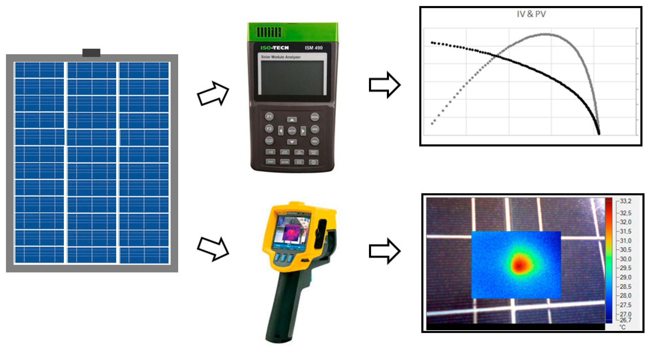
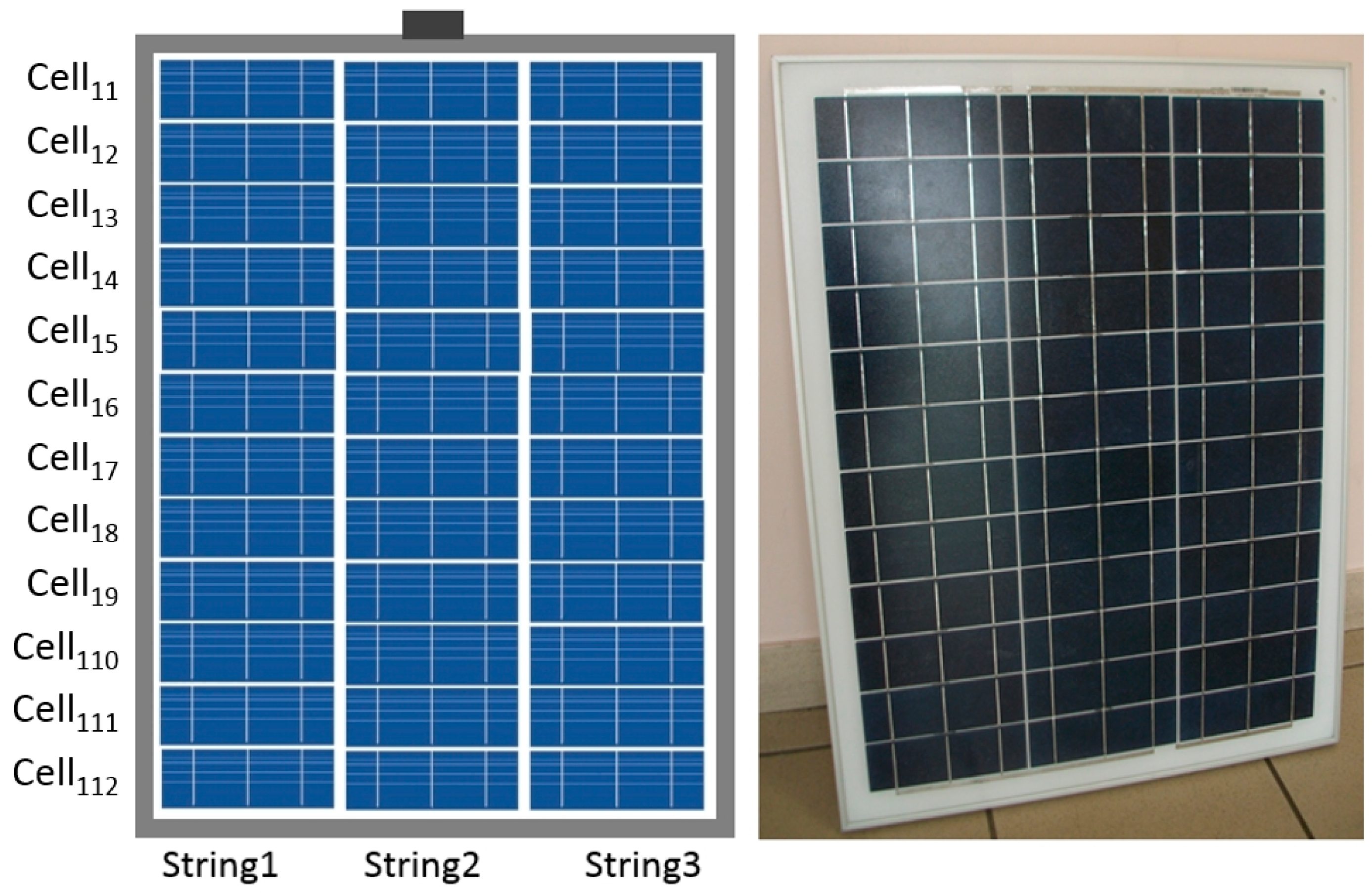
2. Materials and Methods
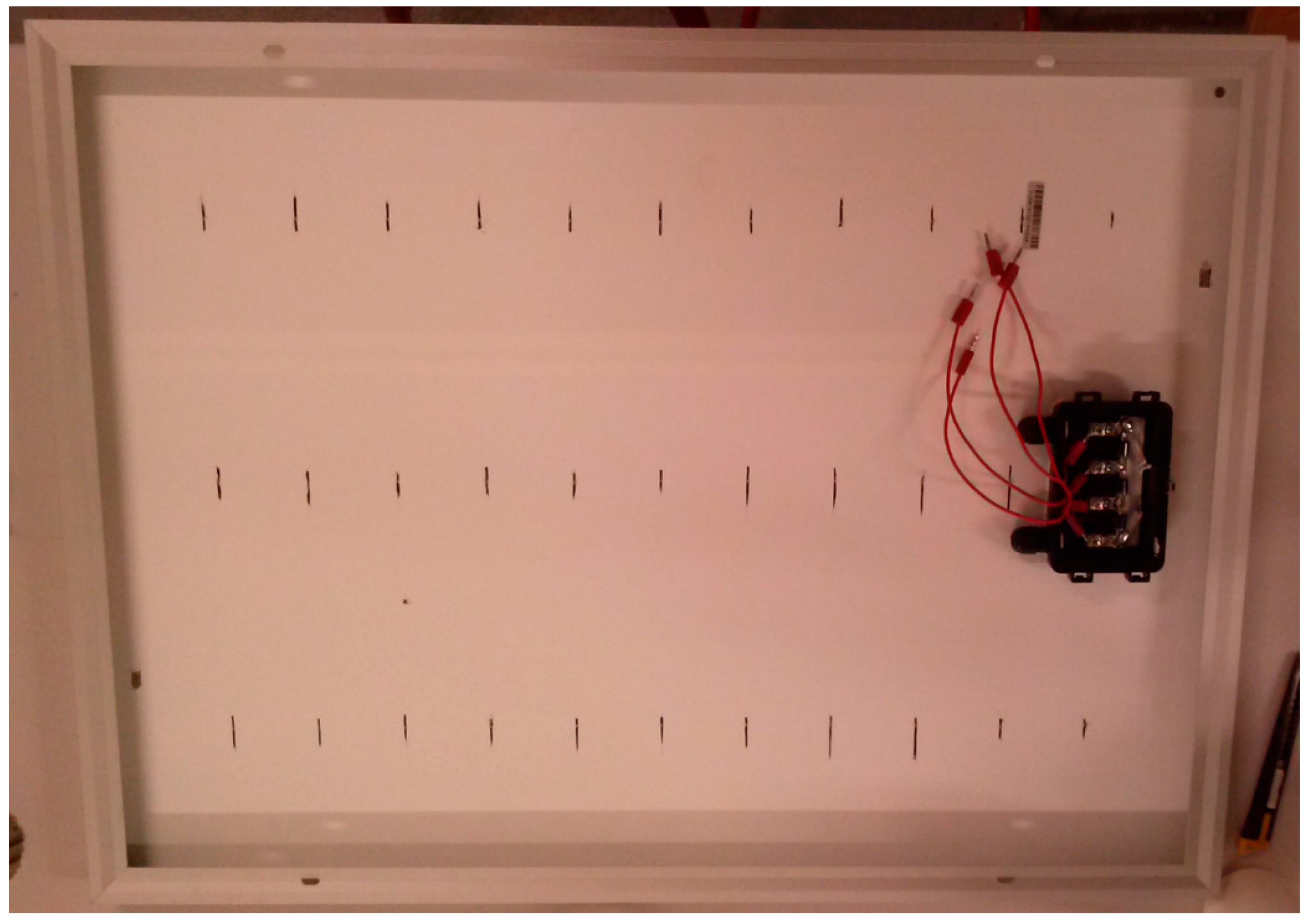
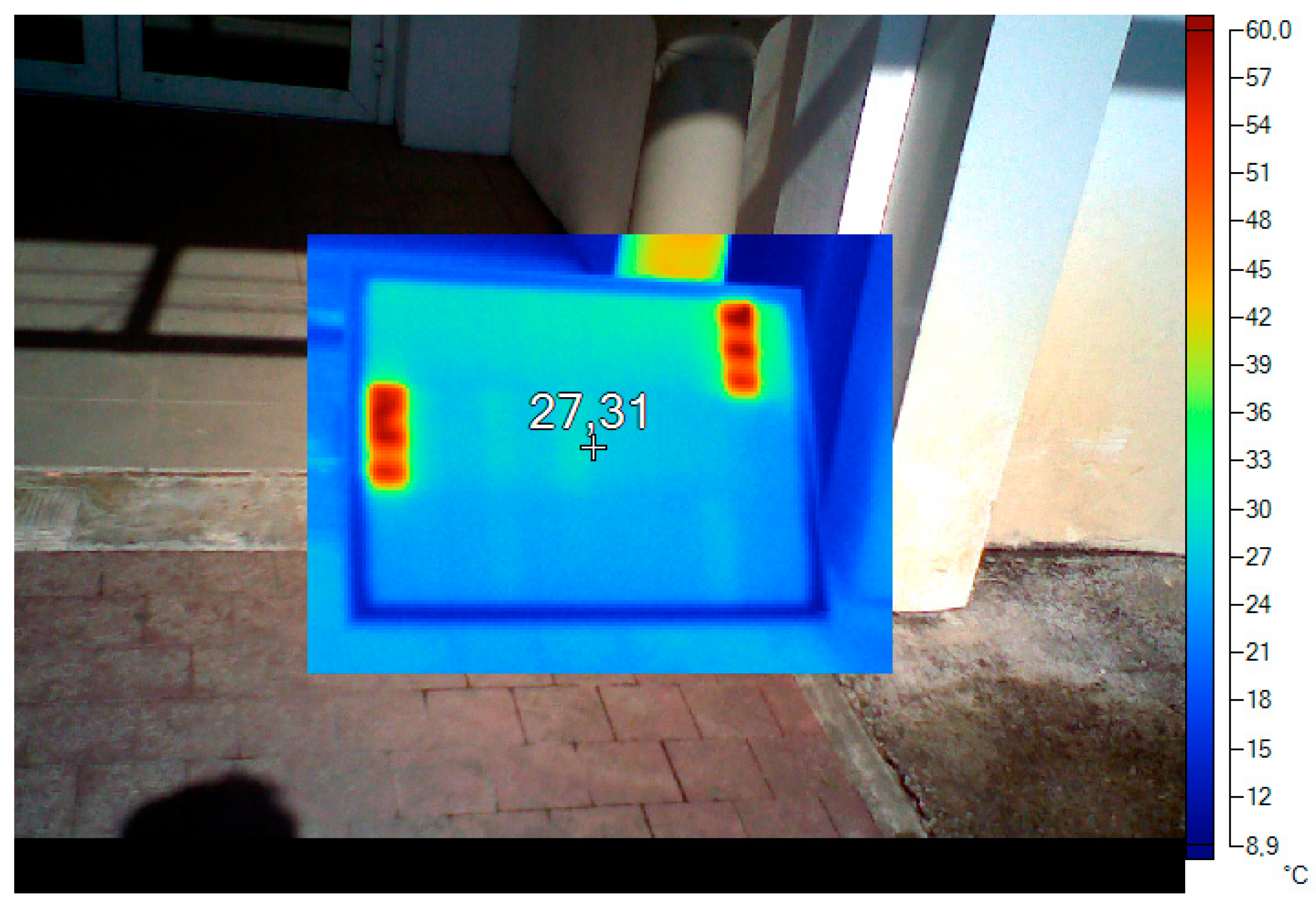
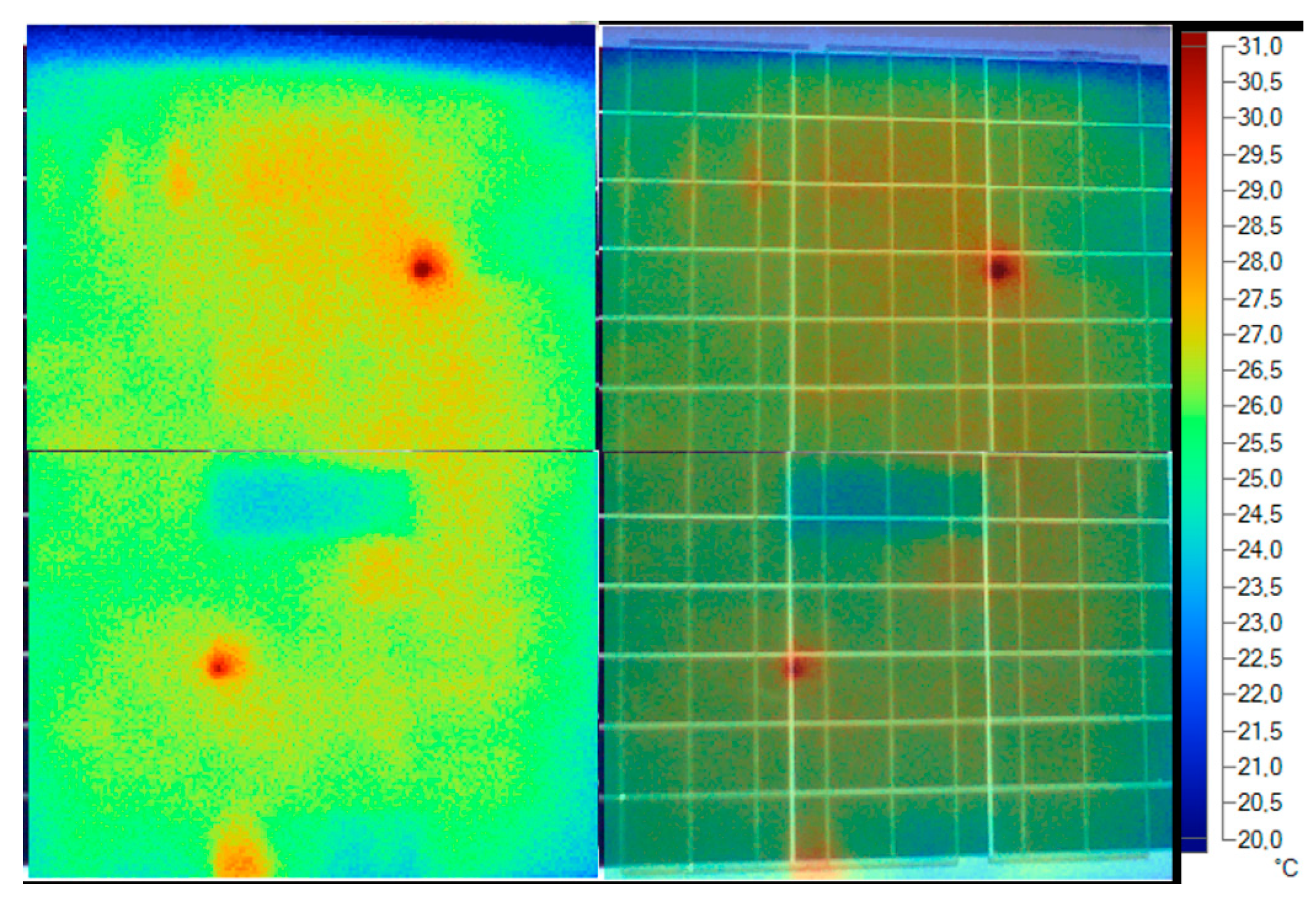
A photovoltaic panel composed of 36 polycrystalline silicon cells of 81.12 cm2 (each of these cells is one third of the 15.6 cm × 15.6 cm common cells) connected in series has been measured and characterized in detail. The characteristics of the panel can be seen in Table 1. Different measurements have been carried out such as thermal images of the module under two different polarization conditions, IV measurements of the panel in order to characterize every cell, and direct IV and resistance measurements of the individual cells (see Figure 3).
The module has three bypass diodes connected in series with one another and to the terminals of the whole panel. Their aim is to bypass the whole module within a larger PV system, but they have no effect on the presented measurements. Although in reality all the cells are connected in series, just for identification, cells in the panel shall be referred to as Cellij, where subscript i represents the string (1, 2 or 3) and subscript j represents the position of the cell within that string (1 to 12)—see Figure 4.

2.1. Thermal Images

First, thermal images of the short-circuited panel were taken under sunlight (measured irradiation between 1084 and 1093 W/m2, around one sun).
Second, for current-applied measurements, the module was moved to the laboratory and 22.4 V (around VMPP) was applied to its terminals. The current for this working condition was 2.25 A. All cells should be around their maximum power point. Thermal images were acquired with a Fluke Ti-10 thermal camera (Fluke Corporation, Everett, WA, USA) [42].

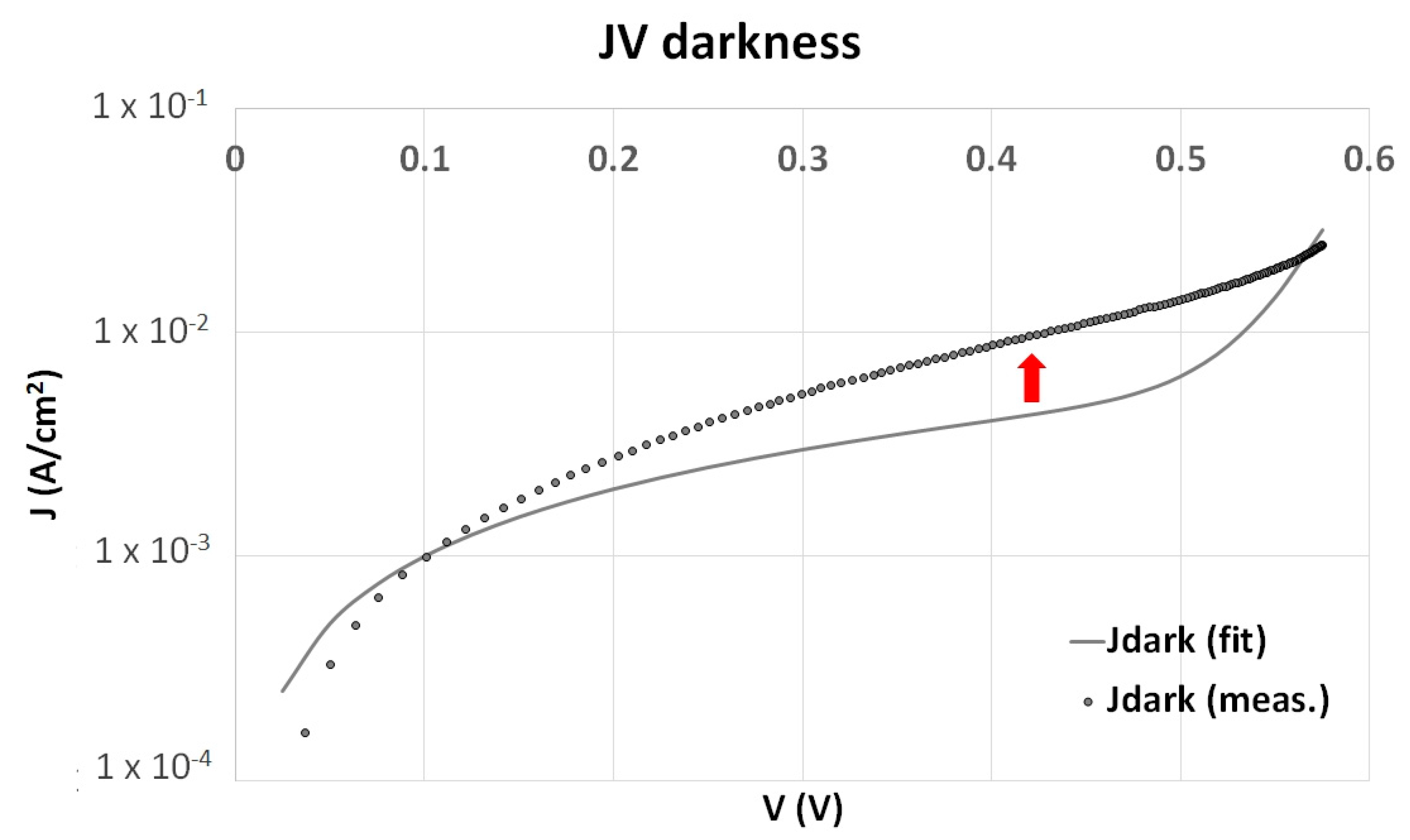
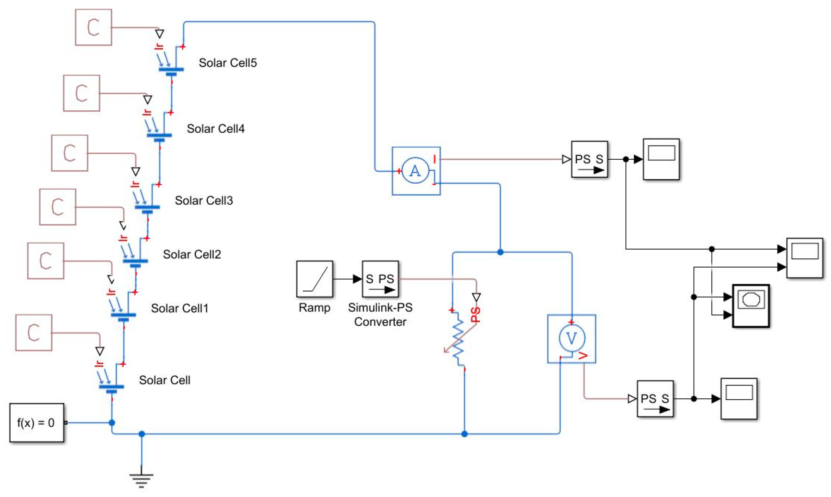
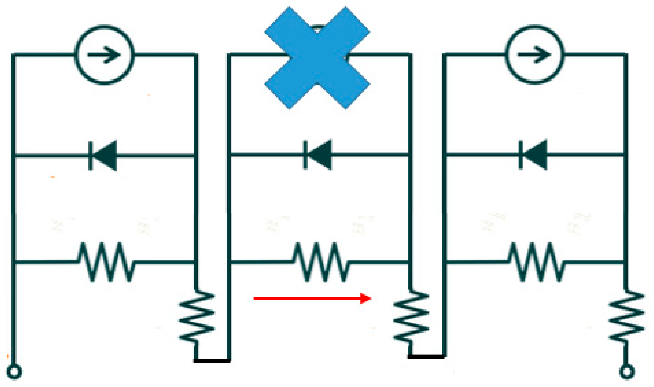
2.2. Module’s IV Curves-Based Method

IV curves of the panel were acquired under sunlight (circa one sun irradiation) with the ISM 490 Solar Module Analyzer of ISO-TECH (Iso-Tech (now RS Pro), Northamptonshire, UK). First, the whole panel was exposed to sunlight and the IV curve of the panel was acquired. Then, the 36 cells were covered, one at a time, as in the IEC 61215 Standard (terrestrial photovoltaic (PV) modules-design qualification and type approval) [43]; the resulting IV curve gives information of the one covered cell [44]. These measurements need to be done quickly because the shadowed cell becomes reverse biased and has to dissipate the power generated by the rest of the cells in the panel. To cover the cells one by one, a cover of the same shape and just slightly bigger than one cell was cut, aiming to completely cover the cell without casting any shadow on the neighboring cells. A small reflection, though, is unavoidable.

2.3. Direct IV Curves

Finally, in order to measure the cells directly, small parts of the rear protective layer of the module were removed. The IV response of the cells was measured using a variable resistor and two multimeters. Not all the cells were accessible: Cell21 and Cell22 lay below the junction box of the module (see Figure 5).

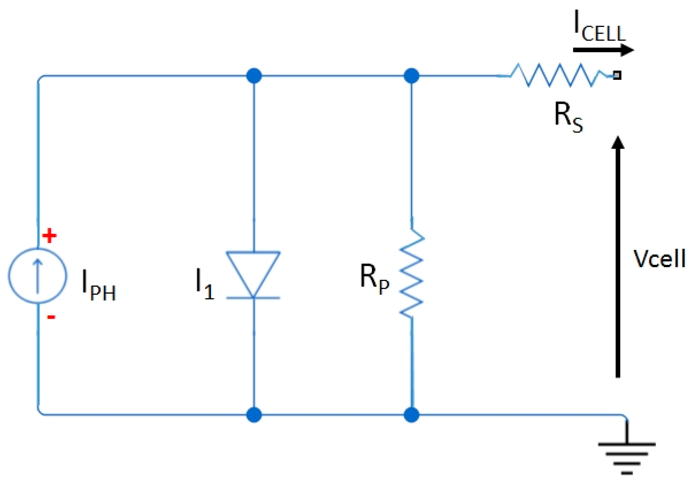
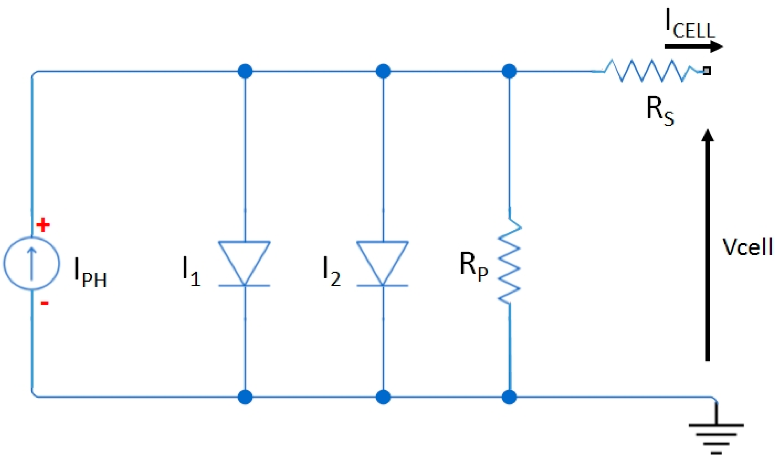
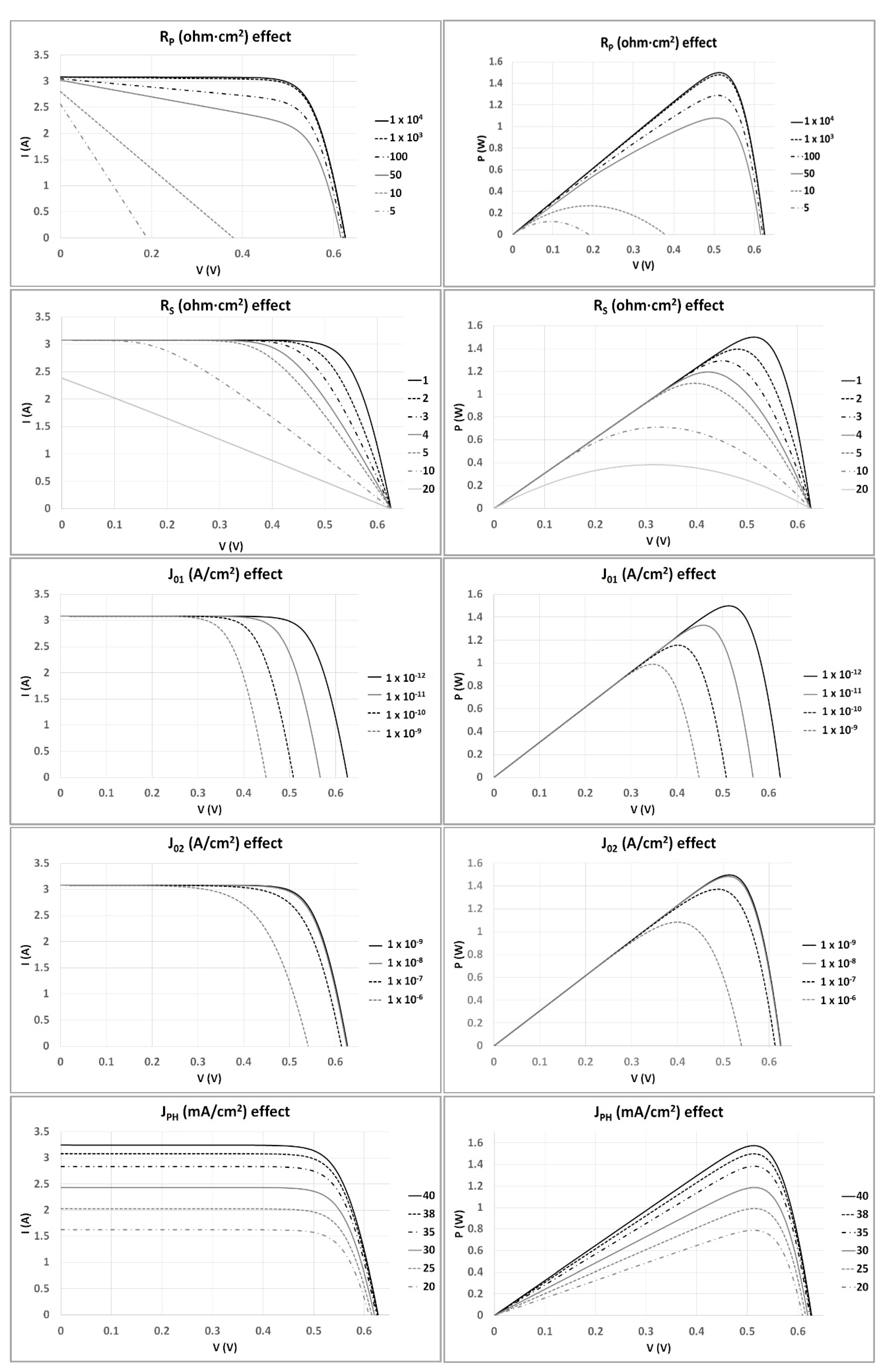
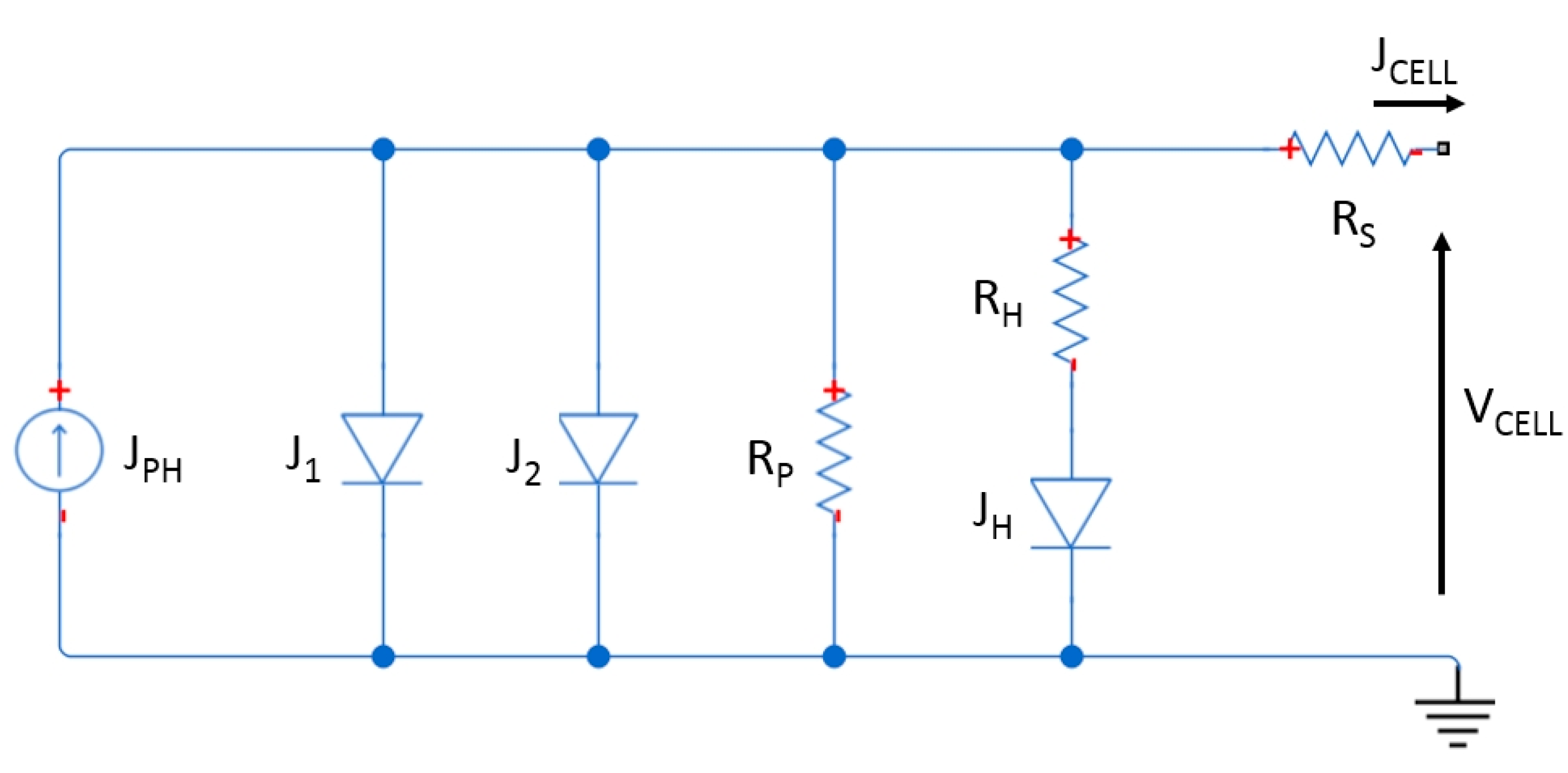
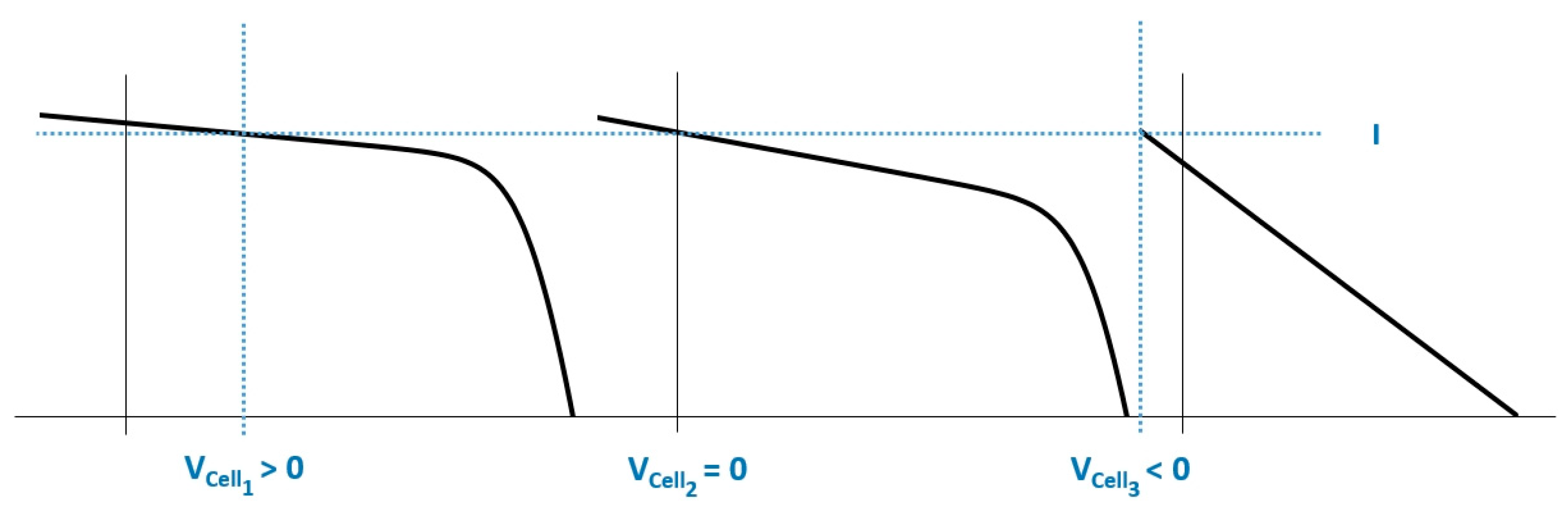
3. Theory/Calculation

In order to compare these experimental measurements to the predicted output, the two-diode model was selected to generate the IV curves using Matlab Simulink (MatlabR2017a, The MathWorks Inc., Natick, MA, USA). According to simulations, a panel with the same dimensions and good parameters (RS = 0.8 Ω·cm2; RP = 97.34 kΩ·cm2; J01 = 1.5 × 10⁻¹² A/cm2; J02 = 1.5 × 10⁻⁸ A/cm2) could provide a power greater than 50 W, as shown in Figure 6. An IV curve with ISC and VOC coincident with those measured, but with a poorer fill-factor (FF), due to higher recombination values (J01 = 7 × 10⁻¹² A/cm2 and J02 = 7 × 10⁻⁸ A/cm2), gives an output power value that could reach as much as 45 W. However, the measurement of the panel shows a rounded IV curve with a very poor FF, resulting in a maximum power output of 28 W (Figure 7).
Using one of the aforementioned cell models, the effect of each of the internal parameters on the output values (VCELL, ICELL, FF and efficiency) and IV characteristic can be checked. Although these effects are known, values going from good to extremely bad were applied to the two-diode cell model in order to show they cannot explain the rounded output of the measured module on their own. Figure 8 shows the results.
Sample normalized values of good parameters are gathered in Table 2. At the end of our study, we show direct IV measurements of the panel cells. We choosed a cell that shows relative good IV curves (Cell23), and fit it. The extracted parameters (J01 = 1.5 × 10⁻¹², J02 = 8 × 10⁻⁸, RP = 10 kΩ·cm2 and RS = 1 Ω·cm2 with RMSE = 0.05) agree quite well with the ones in Table 2.
As the curves in Figure 8 show, all the parameters have an effect on the module’s power output. However, for the most commonly detected failure types (fractured solar cells, faulty soldering, shunted solar cells, etc.) the power reduction comes along with a degradation of the FF. RP and RS are the parameters that have an effect on the FF; but as bad as these are, the IV output does not at all resemble the round-like IV characteristic of the module under study, shown in Figure 7.
Since cells are classified prior to panel mounting, they are all supposed to be similar; and so, the IV curve of a panel, with a generic number n of cells connected in series, could be approximated by the IV curve of one of the cells, having n times its voltage. In this scenario, the whole panel could be modeled by the one-diode [44] or two-diode model [45]. Unfortunately, in general, there will be some mismatch, which could be due to aging or at least to partial shadowing. This effect is shown in Figure 9. The voltage of the measured JV curve of the panel has been divided by the number of cells in series (36 in this case). The JV curve cannot fit into the model of a cell, at least not into the classical one or two-diode models. The smallest RMSE obtained was of 21.38, and corresponds to the fit in Figure 9.
This is because the cells constituting the panel have very different values for the mentioned parameters, making it impossible to fit the whole panel into the model of a single cell. To prove this, a panel of 36 cells was simulated in Matlab. Figure 10 shows the circuit. Each of the symbols (Solar Cell to Solar Cell5) is composed of six identical cells in series. All the cells have the same parameters for the two-diode model, except for the parallel resistance, which has three different values, 0.6 Ω, 0.4 Ω and 0.2 Ω, evenly distributed. The result of the simulations (see Figure 11) fit with a RMSE of 1.82, proving that single cells with different parameter values are the explanation to this round-like IV output; the measured IV output, impossible to obtain with a single cell, is the result of the superposition of the IV curves of cells with different characteristics. For this simulation, different shunt values were chosen because we suspected this to be the non-uniform parameter in our panel. Analogous results could be expected if the difference was found in the photogenerated current, which would be the case of partial shadowing.
Concerning this, in [34], the non-uniform thermal image was analyzed and simulated for the typical defects, and a relation between the defect type, the power loss and the output IV characteristic was investigated.
The behavior of a panel presenting these non-uniformity conditions is equivalent to that of a cell with a lumped shunt, presented by Hernando et al. [46]. The idea is to represent the cell as a compound of unitary cells in parallel, with a resistive series (RS) connection: one of these unitary cells has the bad values that represent the defect—JH in series with RH (Figure 11)—creating a hump in the dark IV curve, like the one present in Figure 12. The third diode allows the modeling of a non-uniform current distribution. Afterwards, this model was applied to a small cell, with the third diode accounting for the peripheral leakage currents [47]. In this latter model, a resistance in series with each diode allows the saturation of their effect at certain bias voltages.
Extrapolating the mentioned circuit model, it could be applied to a panel with rare, seriously damaged cells, provided these are somehow connected in parallel.

4. Results and Discussion

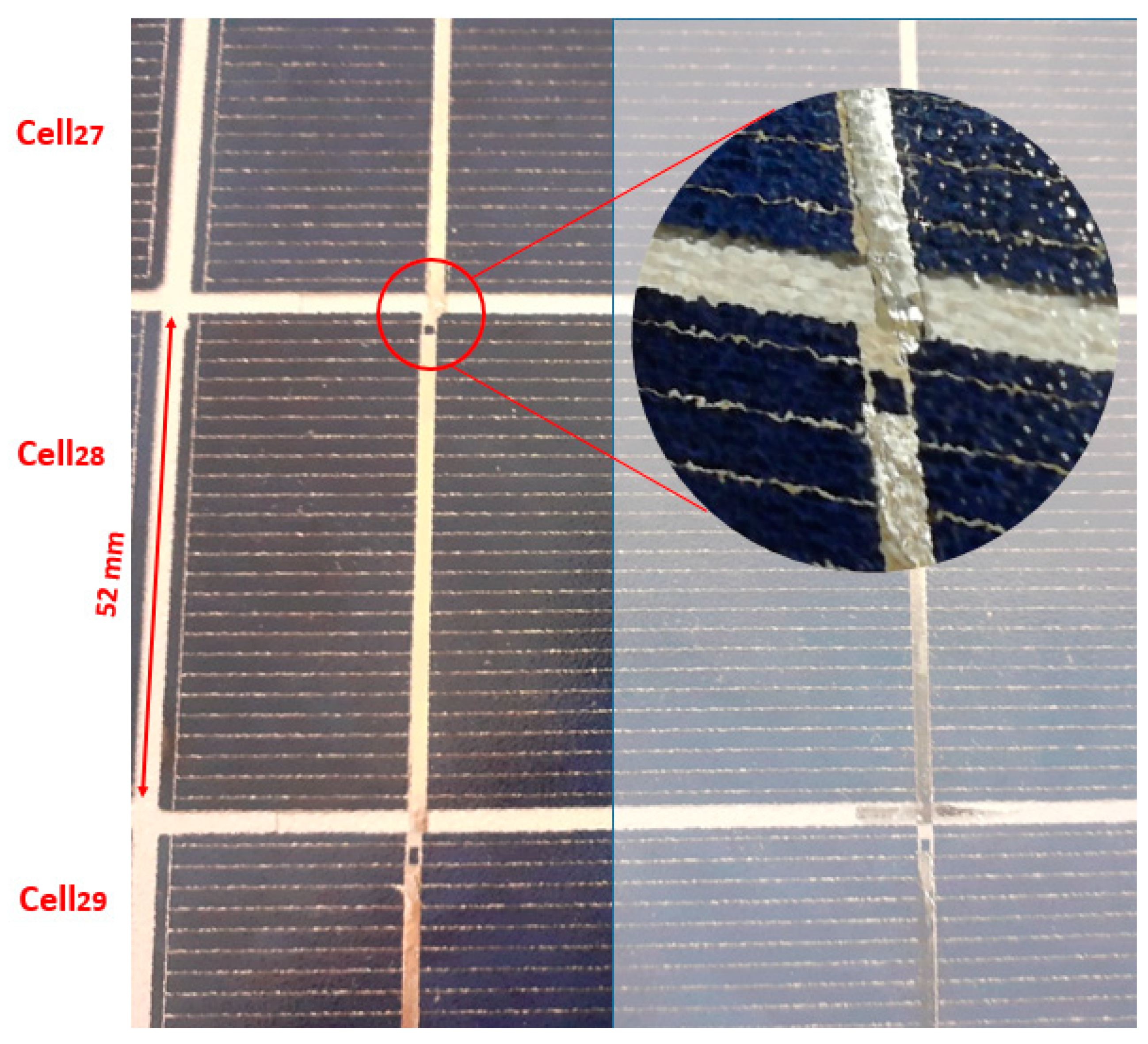
4.1. Module’s Thermal Images

Figure 13 shows thermal images taken outside, with the module short-circuited, under an illumination of approximately one sun (measured 1084 to 1093 W/m2). Two cells stand out because they double the mean temperature of the panel, which indicates they are dissipating more power. Following the aforementioned cell naming system, these cells are Cell12 and Cell212. Given the reduced power output, a thermal pattern of that kind was foreseeable.
On the one hand, as all the cells are connected in series, the same current is going through all of them; on the other hand, since the module is short-circuited, the sum of all individual VCELL must equal zero. Hotter cells probably have a lower photogeneration, and since they are in series, they are forced to work in the negative voltages quadrant to compensate for that (see Figure 14). This does not necessarily mean that these cells are defective, but they are certainly behind the others in terms of photocurrent.
For current-applied measurements, the module was moved to the laboratory and 22.4 V was applied to its terminals (the current for this working condition was 2.25 A). All cells should be around their maximum power point. Recorded images (see Figure 15) reveal localized hot spots at two other cells (Cell29 and Cell33), pointing out small shunts that drain a high current density. Regarding Cell33, a hot spot is visible, but the rest of the cell is cooler than the mean value because the hot spot is sinking a large amount of the current through the cell. These defects can induce a permanent degradation of the cells (and eventually of the whole module), especially if they are located at the corner of the cell, where hot spots are expected to reach higher temperatures [33,48].
Notice that thermal images are shifted with respect to the visible image, as the positions of the hot spots seem to be lower than they really are. Images must not be taken perpendicularly to prevent detection of the reflected light; however, the angle at which pictures are taken does influence the readings slightly. In fact, the hot spots are in the low left corner of Cell29 and Cell33.
The thermal image also shows a cooler cell (Cell27). This means that, for the same current, this cell holds less voltage than the other cells. This cell can be taken as a reference to the misalignment between IR and VIS images. A close visual inspection reveals a soldering misalignment that is short-circuiting Cell27. Figure 16 shows a picture of the area; unfortunately the texturing of the module’s protective glass prevents a sharper image.
Apart from the eye-catching cases of Cell33, Cell27 and Cell29, there are some other cells with uneven temperature distribution: Cell212 and, more faintly, Cell28, or Cell12, which shows increased temperature around the buses, spotting a metallization issue.

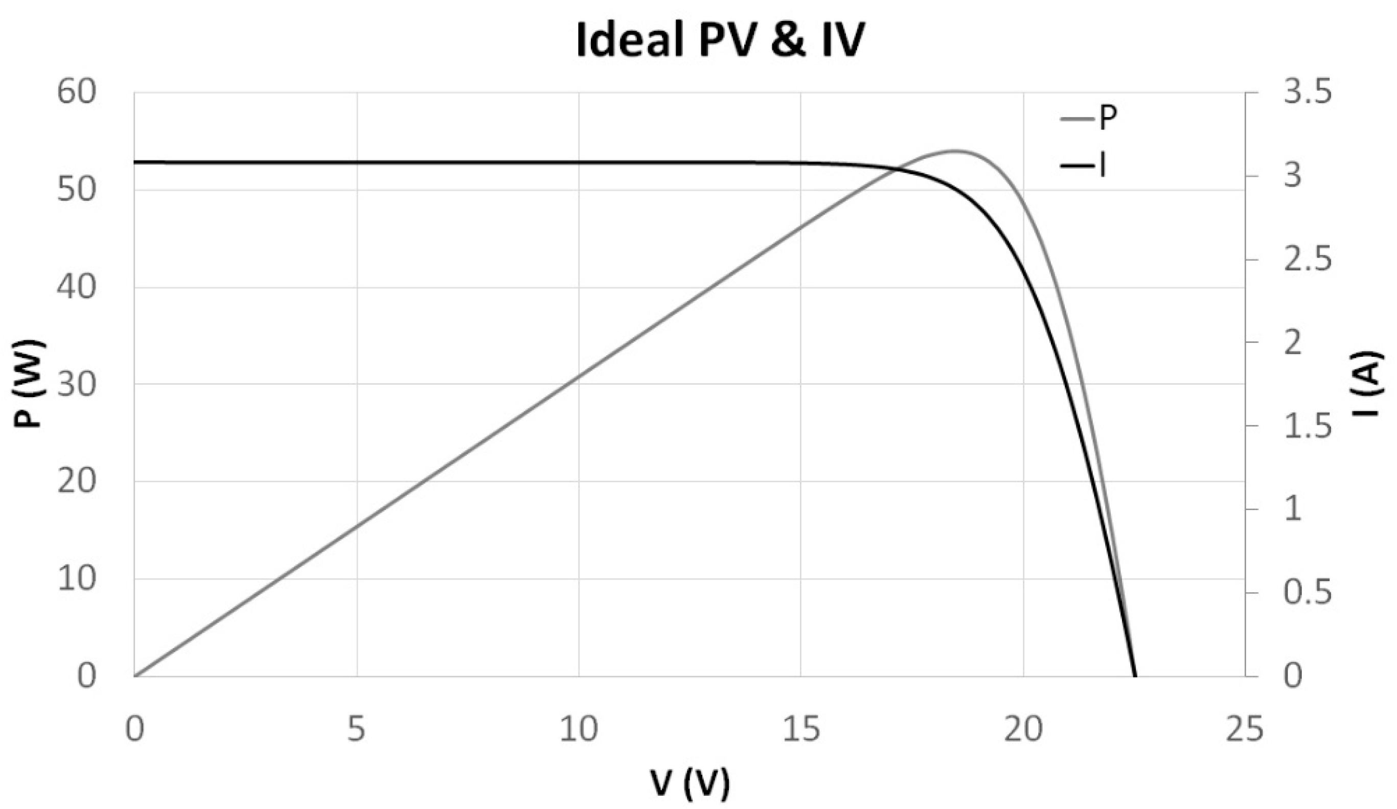
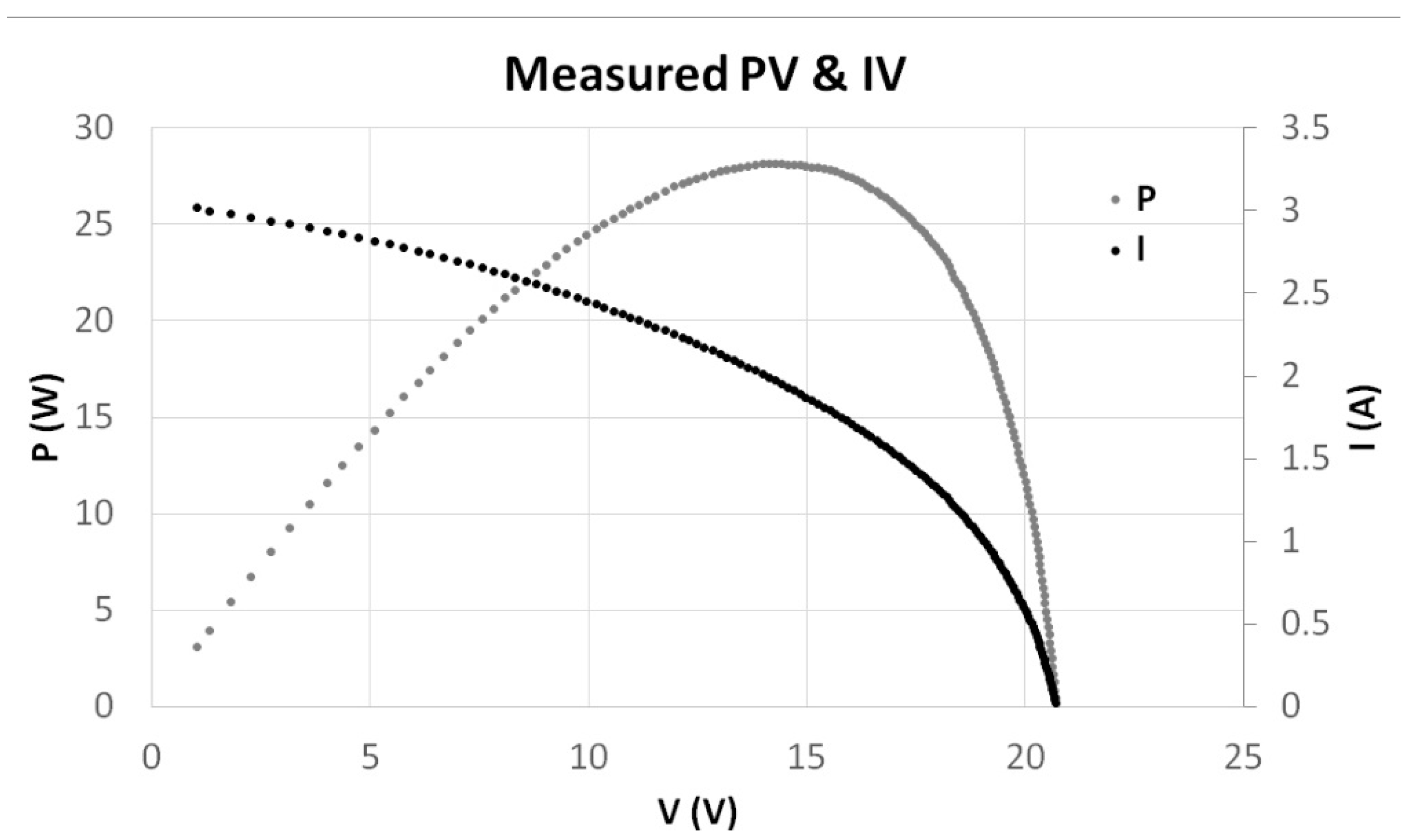
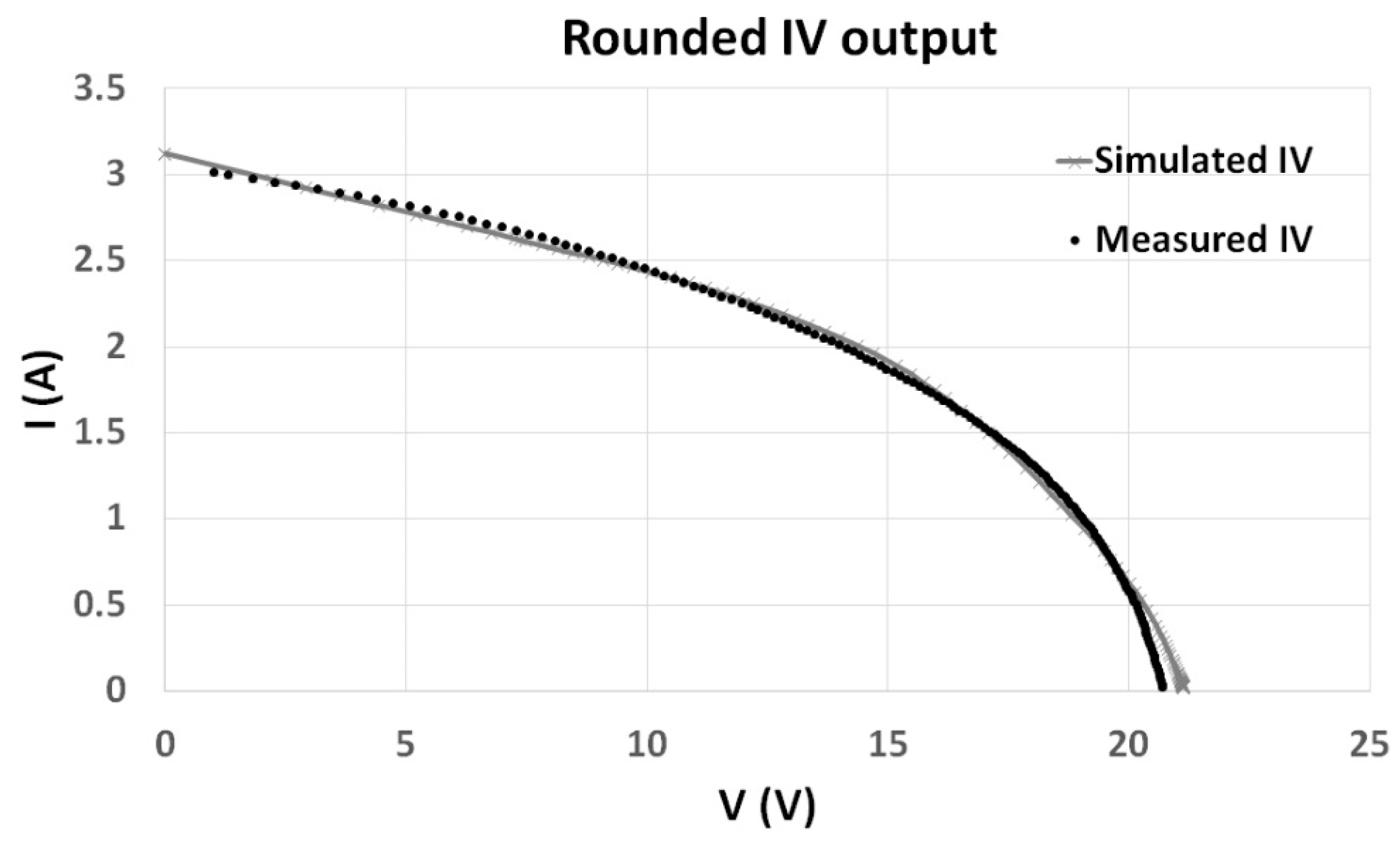
4.2. Module’s IV Curves

The IV characteristic of the module under one sun illumination was taken for different configurations, illuminating the whole module, but also shadowing cells one by one (Figure 17 and Figure 18). This same procedure is proposed in the aforementioned IEC 61215-1-1:2016 international standard [43].
All the measurements show a current offset of around 120 mA (80 mA for cells in the second string), due to the mentioned impossibility of blocking all the sunlight with the cover. The cells in the edge of the module (Celli1, Celli12) show a larger offset, since the white edge of the module and the metallic connections up and down are the most reflective parts of it.
Because all the cells are connected in series, when one of them is shaded (covered), the current is blocked, and the rest of the cells are forced to operate near their VOC. When the applied voltage is near 20 V, the covered cell does not need to stand any reverse voltage (35 cells × VOC ≈ 20 V). For lower applied voltages (15 V for instance), the cells try to move leftward in their IV curve, but the covered cell blocks the current, so they continue near VOC, and the covered cell has to make up the voltage difference (15 − 20 = −5 V). As the applied voltage decreases, the voltage difference increases. There is one point at which the reversed cell breaks down. As can be seen from the graphics at Figure 18, for the cells under study, this breakdown happens between −15 V and −17 V. All the cells in the first string follow this trend, and so do most of the cells in the other two strings, but a few cells in the second and third string show particular behaviors.
A curve parallel to the axis of abscissae indicates a high parallel resistance (good isolation between the p and n areas of the cell), whereas sloppy trends reveal leakages (low parallel resistance), as is the case with Cell12 and Cell212, for example, which showed an irregular thermal distribution in the image in Figure 13.
The values of the second string reveal two severely shunted cells: Cell27 and Cell29. The IV curve obtained when they were covered is similar to the IV output of the uncovered panel. In fact, covering them had almost no effect on the IV curve, since current just went through them (see Figure 18B). As shown in the thermal picture (Figure 13), Cell27 was slightly cooler than the rest and turned out to be short-circuited due to a soldering issue; and Cell29 showed a hot spot.
In the third string, it can be seen that Cell31 is shunted. The other cell showing a hot spot—Cell33—generates a strange output, presenting a snapback behavior [49]. This curve was repeatedly obtained (in the automatic acquisition mode). To check this, some points were taken manually too, showing the voltage going down and then up again, which matches the automatically measured shape. This behavior can be compared to the output of a thyristor, but even if the units are cell thirds (maybe damaged in the cutting step), the formation of an npnp structure seems unlikely. Another possible explanation could be the second breakdown mechanism. Second breakdown was analyzed in the 60 s after recurrent unexpected failures in BJT transistors [50,51,52]. Because the conditions required for this phenomenon are extreme, it has been generally observed after avalanche breakdown, thus the name second breakdown.
Since the first reports on the second breakdown phenomenon, there has been controversy around which are the predominant processes in its initiation. Some researchers advocate the thermal processes over the electronic ones, like Ward [53] or Scarlett, Shockley and Haitz [54]. The latter state that, at a certain critical internal temperature, current density and temperature tend to build up in a small region of the device, resulting in a hot spot. According to Scarlett, Shockley and Haitz, the second breakdown failure observed in most transistors results from the development of a hot spot. In the same vein, Khurana et al. [55] observed that, if the resistivity of a silicon wafer is not uniform, lower resistivity areas will have to withstand a higher current density. The high current density produces a temperature increase at the weak point, which might reach the intrinsic temperature of the junction. Therefore, the thermal voltage will diminish, the current density will be very high at the weak spot, and the temperature might reach values high enough to produce localized melting.
The phenomenon was proven to happen in all junction devices. In solar cells, under reverse bias, inhomogeneous emitters might lead to a local increase in current density and to a drop of junction voltage. If the situation persists, the junction can be damaged, showing a fast and pronounced reduction in voltage. However, in Cell33, the sudden voltage drop occurs as a first, not second, breakdown. From the evidence, it seems the defect in Cell33 is relevant enough to reach this critical point long before avalanche breakdown. More insight into this relationship is necessary to understand the formation and behavior of hot spots in detail, in order to prevent their formation.

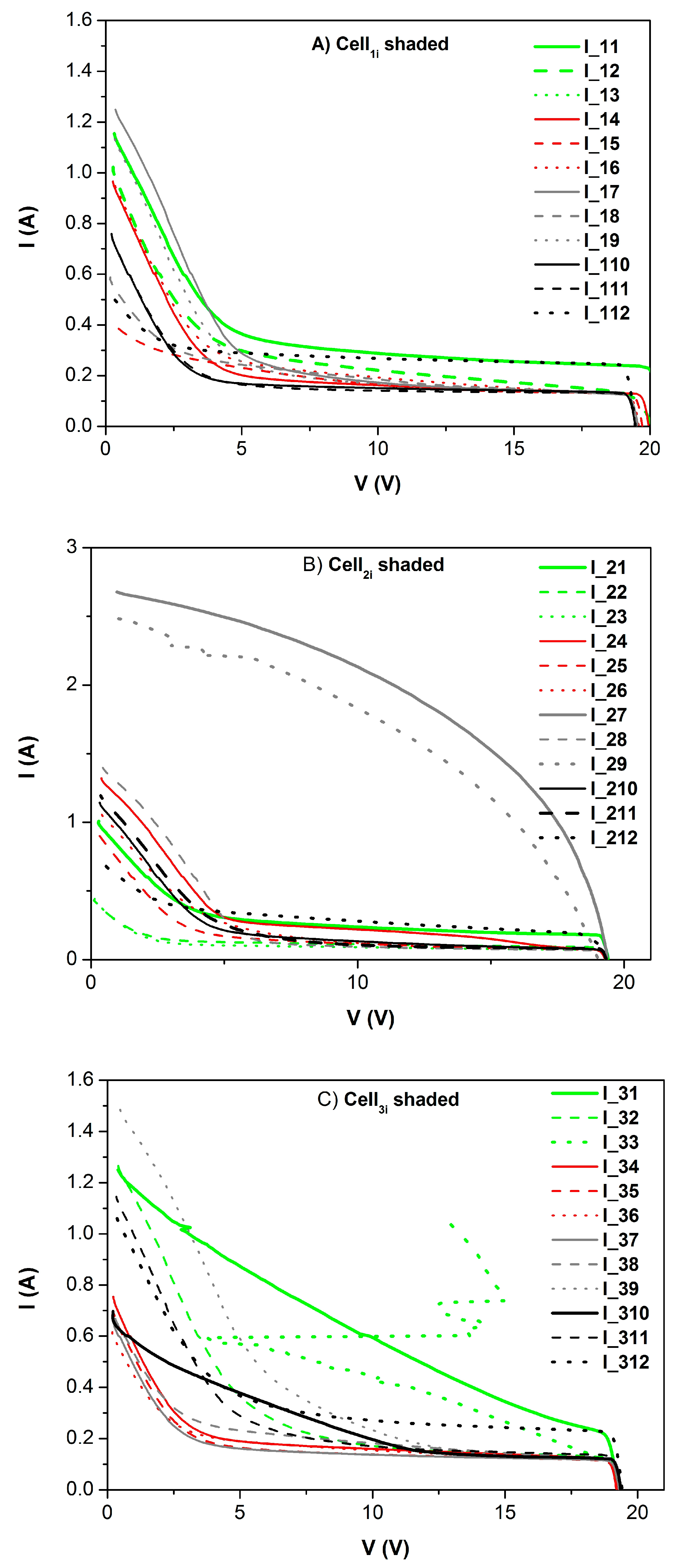
4.3. Individual Cell’s IV Curves

To check the validity of the previous conclusions, some openings were made in the rear of the module to access the cell terminals individually, as described in Section 2.3. Figure 19 shows the measured IV curves of the cells (remember Cell21 and Cell22 remain under the junction box and are not accessible).
IV measurements show that Cell12 and Cell212 have very poor performance, as already deduced from the thermal image of the short-circuited module (Figure 13). The reason is the high GSH, which had already been detected during the reverse bias measurements (Figure 18). Unquestionably, Cell33 is shunted. Remember, Cell27 was discovered to be short-circuited due to a soldering issue. Cell29 shows a poor IV output, but not as bad as could be expected from Figure 18. Surprisingly, Cell211 exhibits a quite worse response.
Cells with good isolation (high RP) exhibit a mostly straight curve: (a) from small voltages towards the maximum power point in Figure 19; and (b) from open circuit downwards, until the breakdown voltage of the cell’s diode is reached in Figure 18. The agreement between both measurements verify the validity of shadowing a cell in a module as a non-invasive way of obtaining individual information on the given cell. Moreover, the conclusions obtained from these measurements are, in general, consistent with the ones extracted from thermal images.

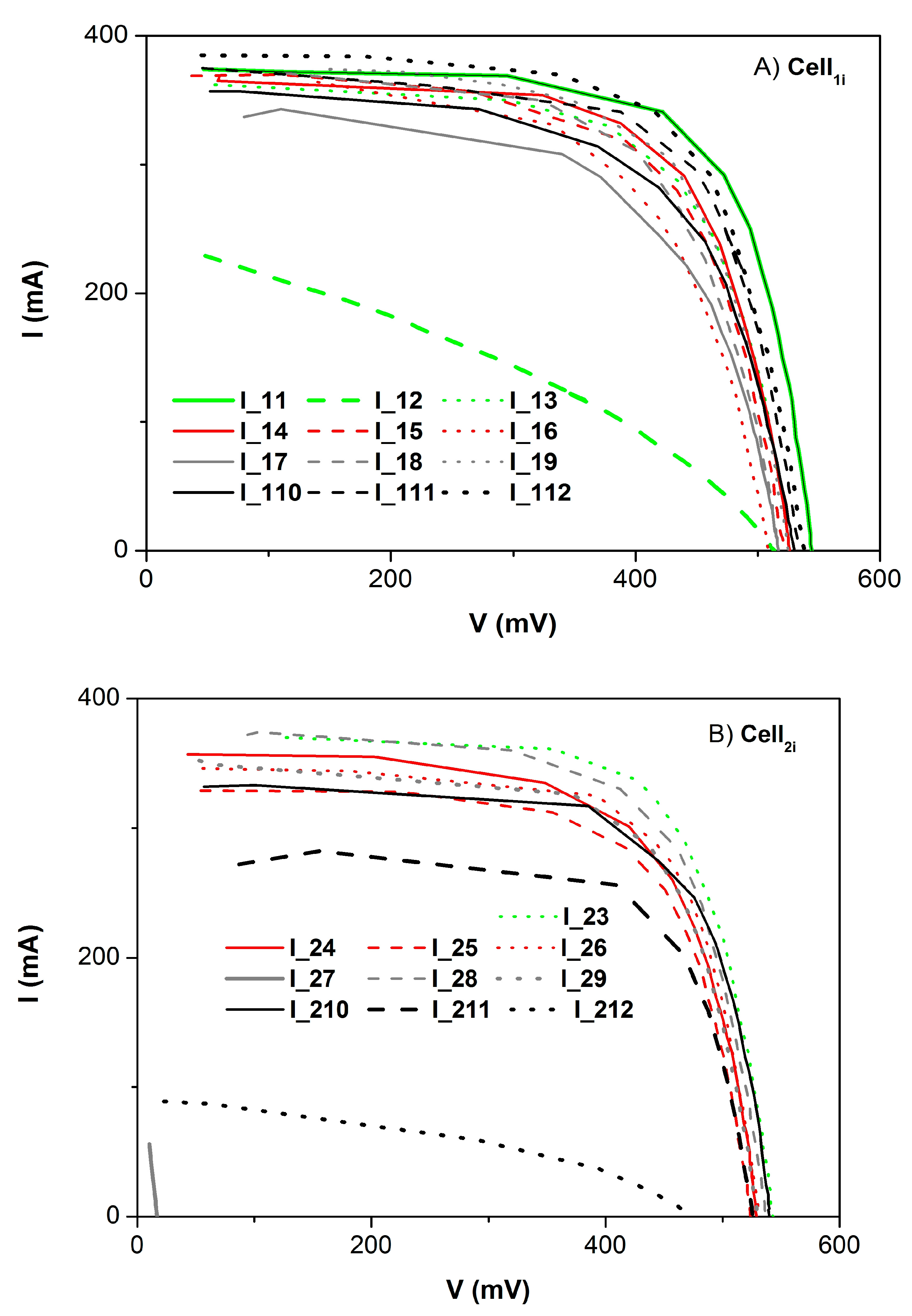
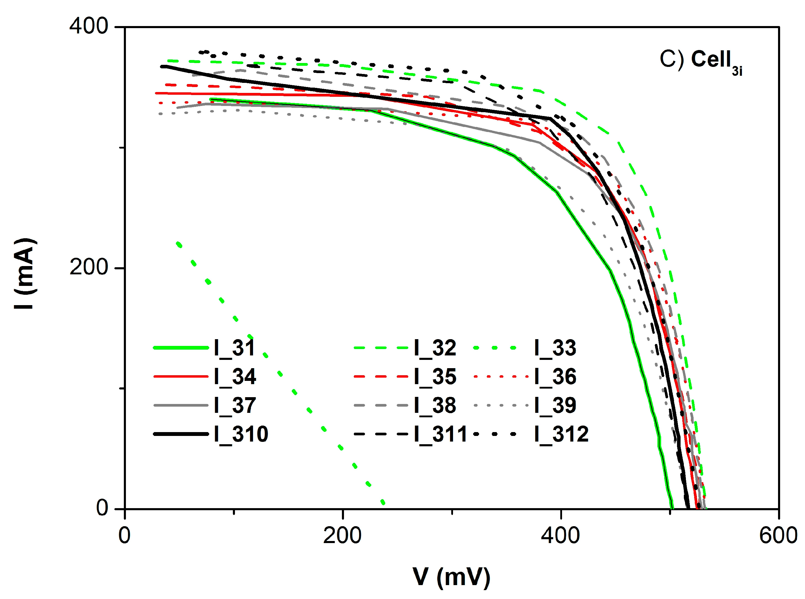
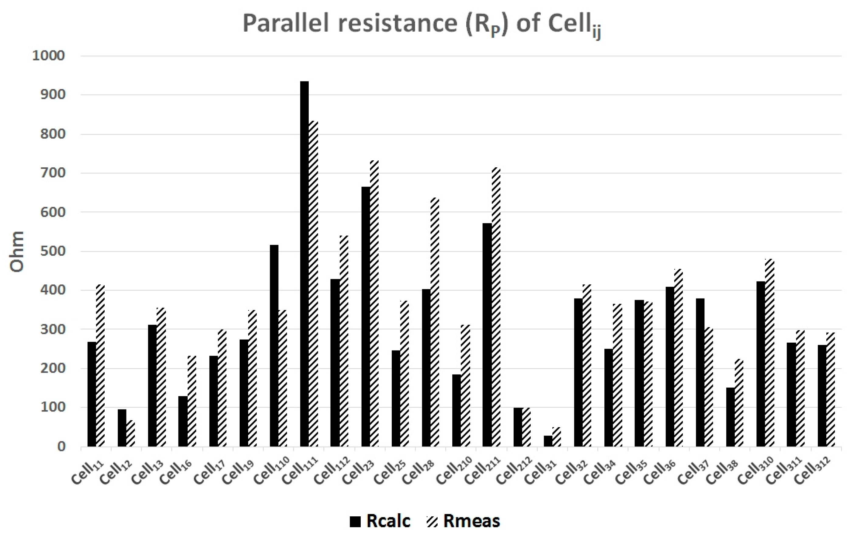
4.4. Individual Cell’s Resistance Measurement

Resistance of the cells accessible by the rear openings were measured with a multimeter. Given the area of the cells under study (≈82 cm2), the value of the parallel resistance for a good cell could be around 100 Ω. This makes the voltage drop induced by the small measuring current of the multimeter to be too small to activate the recombination diodes of the cells (see equivalent circuits in Figure 1, Figure 2 and Figure 11). Consequently, in most cells, the readings are similar for both polarities. A small value for the parallel resistance (RP) is indicative of bad isolation between the p and the n areas of the cell. The slope in the upper part of the IV curve informs on this effect. An extraction of the parallel resistance from Figure 19 does not seem possible; on the other hand, most of the curves in Figure 18 allow an extraction of the slope. This latter value would be related to the parallel resistance of the shaded cell and to the series resistance of the whole module. Although it is assumed that the value of the series resistance will be small, we cannot expect the measured values to be equal to the calculated parallel resistances. However, confronting these calculated slopes with the resistances measured with the multimeter, it is clear that they follow the same trend (see Figure 20; only cells for which measured and calculated values are available are displayed). It was not possible to measure the resistance of cells Cell27 or Cell33, but it can be seen how the worst measurable values of RP for each string correspond to cells with a sloppy IV curve, such as Cell12, Cell212 and Cell31.
As reported elsewhere [19], cells in the same module—supposedly similar—can, however, have very different parallel resistance values, which is a crucial parameter. In our case, some resistance values have been impossible to calculate or measure accurately, but we can state that the module under study undoubtedly presents cells with wide-ranging values for the parallel resistance—the calculated values range from 20 to 920 Ω, and the measured ones from 50 Ω to 830 Ω.

5. Conclusions

Periodic IV measurements of the panel can indicate, by a rounded output, sparsely damaged cells. In this study, we have been able to make a direct comparison between different measurements on the same module. In this context, reverse biased measurements of the cells in the module, obtained by covering the cells individually, have proven to be as good as direct IV curves for the detection of shunted cells. It should be noted that, in particular, in this study, it has been possible to observe thermal breakdown, a mechanism related to hot spots, and which is not normally observed prior to avalanche breakdown. We would like to emphasize the importance of this fact, since we believe that, following the close relationship between both phenomena, we will be able to deepen our understanding of its formation. The final objective is to identify the characteristics of the cells that allow the formation of hot spots, so as to detect them in cells prior to panel mounting.

Author Contributions

Conceptualization, N.A., A.L., O.C. and F.R.; methodology, N.A., A.L., O.C. and F.R.; software, N.A.; validation, N.A., A.L. and O.C.; formal analysis, N.A., A.L. and O.C.; investigation, N.A., A.L. and O.C.; data curation, N.A.; writing—original draft preparation, N.A.; writing—review and editing, N.A. and A.L.; visualization, N.A. and A.L.; supervision, O.C. and F.R. All authors have read and agreed to the published version of the manuscript.

Funding

This research received no external funding.

Institutional Review Board Statement

Not applicable.

Informed Consent Statement

Not applicable.

Data Availability Statement

The data presented in this study are available on request from the corresponding author.

Conflicts of Interest

The authors declare no conflict of interest.

References

  1. Philipps, S.P. Photovoltaics Report. Fraunhofer Institute for Solar Energy Systems ISE. 2021. Available online: https://www.ise.fraunhofer.de/content/dam/ise/de/documents/publications/studies/Photovoltaics-Report.pdf (accessed on 8 February 2022).
  2. Philipps, S.P.; Bett, A.W.; Horowitz, K.; Kurtz, S. Current status of concentrator photovoltaic (CPV) technology. Natl. Renew. Energy Lab. (NREL) 2015. [Google Scholar] [CrossRef]
  3. Sarper, H.; Melnykov, I.; Martínez, L.A. Prediction of daily photovoltaic energy production using weather data and regression. J. Sol. Energy Eng. 2021, 143, 064502. [Google Scholar] [CrossRef]
  4. Doumane, R.; Balistrou, M.; Logerais, P.O.; Riou, O.; Durastanti, J.F.; Charki, A. A circuit-based approach to simulate the characteristics of a silicon photovoltaic module with aging. J. Sol. Energy Eng. 2015, 137, 021020. [Google Scholar] [CrossRef]
  5. Fanney, A.H.; Dougherty, B.P.; Davis, M.W. Comparison of predicted to measured module performance. J. Sol. Energy Eng. 2007, 131, 021011. [Google Scholar] [CrossRef]
  6. Hernández-Callejo, L.; Gallardo-Saavedra, S.; Alonso-Gómez, V. A review of photovoltaic systems: Design, operation and maintenance. Sol. Energy 2019, 188, 426–440. [Google Scholar] [CrossRef]
  7. Triki-Lahiani, A.; Abdelghani, A.B.-B.; Slama-Belkhodja, I. Fault detection and monitoring systems for photovoltaic installations: A review. Renew. Sustain. Energy Rev. 2018, 82, 2680–2692. [Google Scholar] [CrossRef]
  8. Pillai, D.S.; Rajasekar, N. A comprehensive review on protection challenges and fault diagnosis in PV systems. Renew. Sustain. Energy Rev. 2018, 91, 18–40. [Google Scholar] [CrossRef]
  9. Santhakumari, M.; Sagar, N. A review of the environmental factors degrading the performance of silicon wafer-based photovoltaic modules: Failure detection methods and essential mitigation techniques. Renew. Sustain. Energy Rev. 2019, 110, 83–100. [Google Scholar] [CrossRef]
  10. Du, B.; Yang, R.; He, Y.; Wang, F.; Huang, S. Nondestructive inspection, testing and evaluation for Si-based, thin film and multi-junction solar cells: An overview. Renew. Sustain. Energy Rev. 2017, 78, 1117–1151. [Google Scholar] [CrossRef]
  11. Fouad, M.M.; Shihata, L.A.; Morgan, E.I. An integrated review of factors influencing the perfomance of photovoltaic panels. Renew. Sustain. Energy Rev. 2017, 80, 1499–1511. [Google Scholar] [CrossRef]
  12. Hasan, M.A.; Parida, S.K. An overview of solar photovoltaic panel modeling based on analytical and experimental viewpoint. Renew. Sustain. Energy Rev. 2016, 60, 75–83. [Google Scholar] [CrossRef]
  13. Nacar, M.; Özer, E.; Yılmaz, A.E. A six parameter single diode model for photovoltaic modules. J. Sol. Energy Eng. 2021, 143, 011012. [Google Scholar] [CrossRef]
  14. Humada, A.M.; Hojabri, M.; Mekhilef, S.; Hamada, H.M. Solar cell parameters extraction based on single and double-diode models: A review. Renew. Sustain. Energy Rev. 2016, 56, 494–509. [Google Scholar] [CrossRef] [Green Version]
  15. Guo, L.; Meng, Z.; Sun, Y.; Wang, L. Parameter identification and sensitivity analysis of solar cell models with cat swarm optimization algorithm. Energy Convers. Manag. 2016, 108, 520–528. [Google Scholar] [CrossRef]
  16. Chin, V.J.; Salam, Z.; Ishaque, K. Cell modelling and model parameters estimation techniques for photovoltaic simulator application: A review. Appl. Energy 2015, 154, 500–519. [Google Scholar] [CrossRef]
  17. Alonso-Garcia, M.C.; Ruiz, J.M.; Chenlo, F. Experimental study of mismatch and shading effects in the I–V characteristic of a photovoltaic module. Sol. Energy Mater. Sol. Cells 2006, 90, 329–340. [Google Scholar] [CrossRef]
  18. Kaushika, N.D.; Rai, A.K. An investigation of mismatch losses in solar photovoltaic cell networks. Energy 2007, 32, 755–759. [Google Scholar] [CrossRef]
  19. Daliento, S.; Di Napoli, F.; Guerriero, P.; d’Alessandro, V. A modified bypass circuit for improved hot spot reliability of solar panels subject to partial shading. Sol. Energy 2016, 134, 211–218. [Google Scholar] [CrossRef]
  20. Kim, K.A.; Krein, P.T. Hot spotting and second breakdown effects on reverse IV characteristics for mono-crystalline Si photovoltaics. In Proceedings of the IEEE Energy Conversion Congress and Exposition (ECCE), Denver, CO, USA, 15–19 September 2013. [Google Scholar] [CrossRef]
  21. Giaffreda, D.; Magnone, P.; Meneghini, M.; Barbato, M.; Meneghesso, G.; Zanoni, E.; Sangiorgi, E.; Fiegna, C. Local shunting in multicrystalline silicon solar cells: Distributed electrical simulations and experiments. IEEE J. Photovolt. 2014, 4, 40–47. [Google Scholar] [CrossRef]
  22. Dhimish, M. Micro cracks distribution and power degradation of polycrystalline solar cells wafer: Observations constructed from the analysis of 4000 samples. Renew. Energy 2020, 145, 466–477. [Google Scholar] [CrossRef]
  23. Köntges, M.; Kurtz, S.; Packard, C.E.; Jahn, U.; Berger, K.A.; Kato, K.; Friesen, T.; Liu, H.; Iseghem, M.V. Review of Failures of Photovoltaic Modules. International Energy Agency Photovoltaics Power Systems Programme. 2014. Available online: https://iea-pvps.org/key-topics/review-of-failures-of-photovoltaic-modules-final/ (accessed on 8 February 2022).
  24. Bouaichi, A.; Merrouni, A.A.; Hajjaj, C.; Messaoudi, C.; Ghennioui, A.; Benlarabi, A.; Ikken, B.; El Amrani, A.; Zitouni, H. In-situ evaluation of the early PV module degradation of various technologies under harsh climatic conditions: The case of Morocco. Renew. Energy 2019, 143, 1500–1518. [Google Scholar] [CrossRef]
  25. Silva, A.M.; Melo, F.C.; Reis, J.H.; Freitas, L.C.G. The study and application of evaluation methods for photovoltaic modules under real operational conditions, in a region of the Brazilian Southeast. Renew. Energy 2019, 138, 1189–1204. [Google Scholar] [CrossRef]
  26. Dhimish, M.; Mather, P.; Holmes, V. Evaluating power loss and performance ratio of hot-spotted photovoltaic modules. IEEE Trans. Electron Devices 2018, 65, 5419–5427. [Google Scholar] [CrossRef] [Green Version]
  27. Sánchez-Friera, P.; Piliougine, M.; Pelaez, J.; Carretero, J.; Sidrach de Cardona, M. Analysis of degradation mechanisms of crystalline silicon PV modules after 12 years of operation in Southern Europe. Prog. Photovolt. Res. Appl. 2011, 19, 658–666. [Google Scholar] [CrossRef]
  28. Jordan, D.C.; Silverman, T.J.; Wohlgemuth, J.H.; Kurtz, S.R.; VanSant, K.T. Photovoltaic failure and degradation modes. Prog. Photovolt. Res. Appl. 2017, 25, 318–326. [Google Scholar] [CrossRef]
  29. Bauer, J.; Kwapil, W.; Lausch, D.; Schubert, M.C.; Warta, W.; Bothe, K.; Breitenstein, O. Comments on the paper “Detection and analysis of hot-spot formation in solar cells” published by M. Simon and E.L. Meyer in Sol. Energy Mater. Sol. Cells 2010, 94, 106–113. Sol. Energy Mater. Sol. Cells 2012, 99, 362–364. [Google Scholar] [CrossRef]
  30. El Iysaouy, L.; Lahbabi, M.; Baskys, A.; Oumnad, A. Performance analysis of partially shaded photovoltaic array using magic square view configuration for shade dispersion. J. Sol. Energy Eng. 2020, 142, 064502. [Google Scholar] [CrossRef]
  31. Anjum, S.; Mukherjee, V.; Mehta, G. Advanced SuDoKu-based reconfiguration strategies for maximum power extraction from partially shaded solar photovoltaic array. J. Sol. Energy Eng. 2021, 143, 061003. [Google Scholar] [CrossRef]
  32. Trzmiel, G.; Głuchy, D.; Kurz, D. The impact of shading on the exploitation of photovoltaic installations. Renew. Energy 2020, 153, 480–498. [Google Scholar] [CrossRef]
  33. Solheim, H.J.; Fjær, H.G.; Sørheim, E.A.; Foss, S.E. Measurement and simulation of hot spots in solar cells. Energy Procedia 2013, 38, 183–189. [Google Scholar] [CrossRef] [Green Version]
  34. Buerhop, C.; Schlegel, D.; Niess, M.; Vodermayer, C.; Weißmann, R.; Brabec, C.J. Reliability of IR-imaging of PV-plants under operating conditions. Sol. Energy Mater. Sol. Cells 2012, 107, 154–164. [Google Scholar] [CrossRef]
  35. Dhimish, M.; Holmes, V.; Mather, P.; Sibley, M. Novel hot spot mitigation technique to enhance photovoltaic solar panels output power performance. Sol. Energy Mater. Sol. Cells 2018, 179, 72–79. [Google Scholar] [CrossRef] [Green Version]
  36. Dhimish, M.; Holmes, V.; Mehrdadi, B.; Dales, M.; Mather, P. PV output power enhancement using two mitigation techniques for hot spots and partially shaded solar cells. Electr. Power Syst. Res. 2018, 158, 15–25. [Google Scholar] [CrossRef]
  37. Ghosh, S.; Yadav, V.K.; Mukherjee, V. Improvement of partial shading resilience of PV array though modified bypass arrangement. Renew. Energy 2019, 143, 1079–1093. [Google Scholar] [CrossRef]
  38. Tsanakas, J.A.; Ha, L.; Buerhop, C. Faults and infrared thermographic diagnosis in operating c-Si photovoltaic modules: A review of research and future challenges. Renew. Sustain. Energy Rev. 2016, 62, 695–709. [Google Scholar] [CrossRef]
  39. Vumbugwa, M.; Crozier McCleland, J.L.; van Dyk, E.E.; Vorster, F.J. Effects of dynamic operational conditions on thermal infrared imaging of monocrystalline silicon photovoltaic modules. J. Sol. Energy Eng. 2021, 143, 024501. [Google Scholar] [CrossRef]
  40. Bressan, M.; El Basri, Y.; Galeano, A.G.; Alonso, C. A shadow fault detection method based on the standard error analysis of I-V curves. Renew. Energy 2016, 99, 1181–1190. [Google Scholar] [CrossRef] [Green Version]
  41. Zhang, Z.; Wu, J.; Wang, L.; Liu, F.; Jia, P.; Dai, L.; Lu, Y.; Bian, T. The analysis on simulation and invalidation of hot-spot temperature distribution in micro-defective crystalline silicon solar cells. Renew. Energy 2020, 147, 2218–2228. [Google Scholar] [CrossRef]
  42. Fluke Ti10 Infrared Camera. Available online: http://www.myflukestore.com/pdfs/cache/www.myflukestore.com/fluke/thermal_imager/ti10_9hz/manual/fluke_ti10_9hz_thermal_imager_manual.pdf (accessed on 8 February 2022).
  43. IEC System of Conformity Assessment Schemes for Electrotechnical Equipment and Components (IECEE). Available online: https://www.iecee.org/dyn/www/f?p=106:48:0 (accessed on 8 February 2022).
  44. Adamo, F.; Attivissimo, F.; Di Nisio, A.; Lanzolla, A.M.L.; Spadavecchia, M. Parameters Estimation for a Model of Photovoltaic Panels. In Proceedings of the XIX IMEKO World Congress Fundamental and Applied Metrology, Lisbon, Portugal, 6–11 September 2009; Available online: https://www.imeko.org/publications/wc-2009/IMEKO-WC-2009-TC4-622.pdf (accessed on 8 February 2022).
  45. Adamo, F.; Attivissimo, F.; Di Nisio, A.; Spadavecchia, M. Characterization and testing of a tool for photovoltaic panel modeling. IEEE Trans. Instrum. Meas. 2011, 60, 1613–1622. [Google Scholar] [CrossRef]
  46. Hernando, F.; Gutierrez, R.; Bueno, G.; Recart, F.; Rodriguez, V. Humps, a surface damage explanation. In Proceedings of the 2nd World Conference and Exhibition on Photovoltaic Solar Energy Conversion, Vienna, Austria, 6–10 July 1998. [Google Scholar]
  47. Nishioka, K.; Sakitani, N.; Uraoka, Y.; Fuyuki, T. Analysis of multicrystalline silicon solar cells by modified 3-diode equivalent circuit model taking leakage current through periphery into consideration. Sol. Energy Mater. Sol. Cells 2007, 91, 1222–1227. [Google Scholar] [CrossRef]
  48. Ramspeck, K.; Schenk, S.; Duphorn, D.; Metz, A.; Meixner, M. In-line thermography for reliable hot spot detection and process control. Energy Procedia 2014, 55, 133–140. [Google Scholar] [CrossRef] [Green Version]
  49. Schafft, H.A. Second breakdown—A comprehensive review. Proc. IEEE 1967, 55, 1272–1288. [Google Scholar] [CrossRef]
  50. Smith, W.B.; Pontius, D.H.; Budenstein, P.P. Second breakdown and damage in junction devices. IEEE Trans. Electron Devices 1973, 20, 731–744. [Google Scholar] [CrossRef]
  51. Schafft, H.A.; French, J.C. “Second breakdown” in transistors. IRE Trans. Electron Devices 1962, 9, 129–136. [Google Scholar] [CrossRef]
  52. Mars, P. Some aspects of the p-n junction second-breakdown mode. PI Electr. Eng. 1969, 116, 1860–1862. [Google Scholar] [CrossRef]
  53. Ward, A. Studies of second breakdown in silicon diodes. IEEE Trans. Parts Hybrids Packag. 1977, 13, 361–368. [Google Scholar] [CrossRef]
  54. Scarlett, R.M.; Shockley, W.; Haitz, R.H. Thermal instabilities and hot spots in junction transistors. In Proceedings of the First IEEE Annual Symposium on the Physics of Failure in Electronics, Chicago, IL, USA, 26–27 September 1962. [Google Scholar] [CrossRef]
  55. Khurana, B.S.; Sugano, T.; Yanai, H. Thermal breakdown in silicon p-n junction devices. IEEE Trans. Electron Devices 1966, 13, 763–770. [Google Scholar] [CrossRef]
Figure 1. One-diode circuit model.
Electronicmat 03 00014 g001
Figure 2. Two-diode circuit model.
Electronicmat 03 00014 g002
Figure 3. Materials and measurement types.
Electronicmat 03 00014 g003
Figure 4. Identification of cells in the module (left) and picture of the real module (right).
Electronicmat 03 00014 g004
Figure 5. Incisions in the rear of the module.
Electronicmat 03 00014 g005
Figure 6. IV and PV curves of a panel simulated in Matlab with the same ISC and VOC of the measured panel, and good recombination characteristics (RS = 0.8 Ω·cm2; RP = 97.34 kΩ·cm2; J01 = 1.5 × 10⁻¹² A/cm2; J02 = 1.5 × 10⁻⁸ A/cm2).
Electronicmat 03 00014 g006
Figure 7. Measured IV and PV curves of the panel under study.
Electronicmat 03 00014 g007
Figure 8. Effect of the parameters of the two-diode model of a cell on its IV and PV outputs (unless otherwise specified in the graphic, the values are RP = 10 kΩ·cm2; RS = 1 Ω·cm2; J01 = 1 × 10⁻¹² A/cm2; J02 = 1 × 10⁻⁹ A/cm2; JPH = 40 mA/cm2).
Electronicmat 03 00014 g008
Figure 9. Measured darkness (recombination) JV curve (meas.) showing a hump and the fitting essay (fit.) using the two-diode model (J01 = 5 × 10⁻¹² A/cm2, J02 = 1 × 10⁻⁸ A/cm2, RP = 100 Ω·cm2, RS = 1 mΩ·cm2 and JPH = 26 mA/cm2; these are the parameter values obtained for the best fit, RMSE = 21.38).
Electronicmat 03 00014 g009
Figure 10. Matlab simulation of a panel composed of 36 cells (6 groups of 6 identical cells) in series. Each of these groups of cells has a value for the parallel resistance that can be 0.2 Ω, 0.4 Ω or 0.6 Ω.
Electronicmat 03 00014 g010
Figure 11. IV curves of the measured module and the output of a module simulated in Matlab (36 cells with IPH = 3.2 A and RS = 0.01 Ω), with good recombination values (I01 = 1.2 × 10⁻¹⁰ mA and I01 = 1.2 × 10⁻⁶ mA) and 3 different RP evenly distributed (RP1 = 0.6 Ω, RP2 = 0.4 Ω and RP3 = 0.2 Ω).
Electronicmat 03 00014 g011
Figure 12. Circuital model of a module with a severely damaged cell.
Electronicmat 03 00014 g012
Figure 13. Thermal images of the panel exposed to sunlight. Cell12 and Cell212 are significantly hotter than the rest.
Electronicmat 03 00014 g013
Figure 14. Cells connected in series (same current) working at different voltages.
Electronicmat 03 00014 g014
Figure 15. Thermal images of the panel applying a 22.4 V voltage. Images on the left show only IR; the ones on the right show 50% IR and 50% VIS.
Electronicmat 03 00014 g015
Figure 16. Bad soldering between Cell27 and Cell28.
Electronicmat 03 00014 g016
Figure 17. Shadowed cell in a series connection.
Electronicmat 03 00014 g017
Figure 18. IV measurements (@ 1 sun) with only one cell covered (A) first string, (B) second string and (C) third string (remember the 36 cells, the 3 strings, are connected in series).
Electronicmat 03 00014 g018
Figure 19. Manual IV of cells in string (A) 1, (B) 2 and (C) 3. The irradiation (not calibrated) is the same for all the cells.
Electronicmat 03 00014 g019aElectronicmat 03 00014 g019b
Figure 20. Manually measured resistances of some cells (Rmeas) vs. resistances calculated from the slopes in Figure 18 (Rcalc).
Electronicmat 03 00014 g020
Table 1. Characteristics of the PV panel.
ParameterValue
MaterialPolycrystalline Silicon
Number of cells36
Maximum Power (W)50
VOC (V)22.5
ISC (A)3.02
VMP (V)18.32
IMP (A)2.94
Cell size (mm2)156 × 52
Table 2. Example values of the internal parameters of a good cell.
RP (Ω·cm2)RS (Ω·cm2)J01 (A/cm2)J02 (A/cm2)
1 × 10411 × 10−121 × 10−9
Low parallel
conductivity (no shunts)
Low series resistance
(good contact)
Low recombination diodes’ saturation currents
Publisher’s Note: MDPI stays neutral with regard to jurisdictional claims in published maps and institutional affiliations.

