1. Introduction
Surface plasmon polaritons (SPPs) represent a unique class of electromagnetic waves, arising from the interaction between the free electrons excited by light on a metal surface and photons within a dielectric medium [
1]. Their behavior is influenced by specific conditions such as the frequency, angle of incidence, and polarization direction of the incoming light, aligning with the vibrational modes of the surface plasmons on the metal. Both the propagation speed and wavelength of SPPs are contingent upon the characteristics of the metal surface and the refractive index of the medium. SPPs exhibit sub-wavelength scale propagation properties, localized field enhancement effects, and sensitivity around the metal surface, making them extensively applicable in the realm of optical detection [
2,
3].
The localized field enhancement effects of SPPs serve to amplify spectroscopic phenomena such as Raman scattering and fluorescence. Furthermore, as SPPs propagate along a metal surface, they experience attenuation in the direction of light propagation. This positions SPPs as an exceptionally sensitive tool for sensing applications. For instance, they are employed in surface enhanced Raman scattering (SERS) for the high-sensitivity detection of molecules, as well as in surface plasmon resonance sensors, microscopy imaging, and photonic devices [
4]. Additionally, they hold potential utility in photovoltaic technologies, capable of enhancing the efficiency of solar cells. These applications leverage the unique characteristics and effects of SPPs, unveiling new possibilities for research and application across various domains [
5].
In recent years, metal–insulator–metal (MIM) waveguide structures have demonstrated the capability to confine and guide surface plasmon polaritons (SPPs), enabling the effective localization of light fields between the metal surface and the insulator [
6,
7]. This facilitates the enhancement of electromagnetic fields on the metal surface, thereby promoting the generation of SPPs. The metal in these structures provides free electrons to support the propagation of SPPs, while the insulator prevents energy leakage of SPPs into the surrounding medium, achieving efficient transmission of SPPs [
8].
The structural parameters of MIM waveguides significantly influence the propagation characteristics of SPPs, such as the type of metal, the refractive index of the insulator, and the dimensions of the waveguide [
9]. By adjusting these parameters, one can control and tune the propagation speed, wavelength, and transmission losses of SPPs. Therefore, this structure, capitalizing on the interactions among the metal, insulator, and their interface, serves as a key direction for optimizing nano-scale sensor structures. It enables the effective manipulation and application of SPPs [
10].
For example, Rashid et al. proposed a refractive index sensor based on the coupling of three circular rings, achieving a maximum sensitivity of 3573.3 nm/RIU with Figure of merit (FOM) of 21.9 [
11]. Kazanskiy et al. introduced a semi-circular resonator loaded with periodically decorated nano-dots, achieving an optimal sensitivity of 1084.21 nm/RIU [
12].
Wang et al. presented a circular open-ring resonator structure, with a maximum sensitivity of 1114.3 nm/RIU and Figure of merit (FOM) of 55.71 [
13]. Khani and Hayati designed elliptical resonators with sensitivities up to values of up to 550 nm per refractive index unit, with a high FOM value of 282.5 RIU
−1 near the resonance wavelength of 592 nm [
14]. Rakhshani analyzed a compact refractive index sensor in 2-D plasmonic waveguide by hexagonal-ring cavity. The temperature sensitivity values were up to 4270 nm/refractive index unit (RIU) and 0.56 nm/°C, respectively [
15].
“nm/RIU” stands for nanometers per refractive index unit. This unit represents the amount of wavelength change in nanometers corresponding to a change in refractive index unit. It is used to indicate the resolution and sensitivity of optical sensors in detecting changes in the refractive index of a medium.
In plasmonic-waveguide coupling systems, a variety of optical phenomena can be observed, such as dispersion effects, Fano resonances, surface plasmon resonances, and more. Fano resonance plays a crucial role in these plasmonic-waveguide coupling systems. Near the surface of a metal, free electrons oscillate under the excitation of incident light, forming plasmonic vibrations [
16]. Fano resonance is a result of the interaction between these plasmonic vibrations and waveguide modes. When their wavelengths match those of the waveguide modes, intense coupling occurs, leading to the emergence of Fano resonance. When a continuous background scattering spectrum overlaps with a discrete spectral line, Fano resonance appears.
Bright mode and dark mode are two modes related to the phenomenon of optical resonance, which together form the Fano resonance. The bright mode is the main optical mode contributing to the Fano resonance and is characterized by the formation of distinct peaks in the spectral lines. When propagating and transmitted waves are in phase and superimposed, they are coherently enhanced at specific wavelengths, forming a peak; the bright mode. The bright mode is usually represented by a peak in the Fano resonance spectral line, indicating a significant increase in light intensity at this wavelength. The dark mode is another optical mode in the Fano resonance and is characterized by the formation of a valley or trough in the Fano resonance spectral line [
17,
18].
Dark mode corresponds to a situation where the propagating and transmitting waves are in opposite phase or out of phase in the optical structure. When propagating and transmitting waves are phase-opposed and out of phase, they coherently cancel out at a specific wavelength, forming a valley; the dark mode. The dark mode usually manifests itself as a trough in the Fano resonance spectral line, indicating a significant reduction in light intensity at this wavelength. The combination of these two modes gives the Fano resonance a flexible tuning property in different applications and can be used in optical applications such as sensing, filtering, and modulation [
19,
20].
In this study, based on the properties of optical Fano resonances and the plasmonic-waveguide coupling system, we propose a novel nano-scale refractive index sensor structure comprising an MIM waveguide and a DTR cavity. We employed the finite element method (FEM) and coupled-mode theory to comprehensively evaluate the propagation characteristics of the entire structure, both of which can analyze the propagation and coupling of waveguide modes.
The simulation results indicated that the presence of a rectangular stub introduces non-uniformity in the transverse dimensions of the waveguide. This non-uniformity can alter the propagation path and mode distribution of electromagnetic waves in the waveguide, resulting in broadband characteristics in the frequency domain. Double-tooth ring and metal waveguide coupling structures are designed to produce a narrow band in the frequency domain by virtue of their unique geometry and material parameters. This means that only light waves in a specific frequency range can be effectively propagated and coupled. Due to the overlap in frequency between continuous broadband modes and discrete narrowband modes, this interference results in asymmetric waveform characteristics, leading to an asymmetric Fano resonance waveform.
We studied the influence of variations in refractive index and structural geometric parameters on the transmission characteristics, including the rotation angles, the width between the double-tooth rings, and the gap between the DTR cavity and the waveguide. The results showed that different geometric parameters have varied impacts on the transmission curve, the bandwidth of the system, and the performance indicators of the system. Moreover, based on the optimized structural parameters identified, the maximum sensitivity and Figure of merit (FOM) coefficient obtained demonstrate excellent sensitivity and refractive effects for oil concentration detection in industrial oil–water mixtures.
2. Materials and Methods
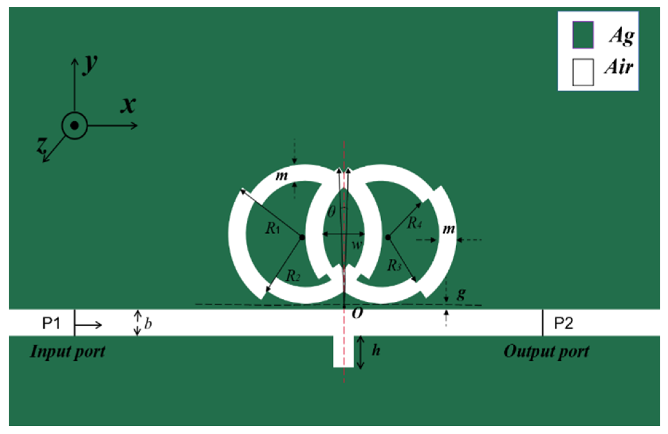
Figure 1 is a plan view of the entire coupled cavity and the composition of the dielectric material. The coupling structure consisted of an MIM waveguide and DTR cavity. As shown in
Figure 1, the green portion utilizes silver metal material as the substrate because it can effectively conduct electromagnetic waves, has low optical losses, and reduces energy loss. The white portion represents the air medium. The relative permittivity of air is
, and the relative permittivity of metallic silver is defined as follows [
21,
22]:
In the equation, the explanation of parameter values is infinite frequency relative permittivity = 3.8344, static dielectric strength = −9530.5, slack time τ = 7.4 × 10⁻¹⁵ s, and electrical conductivity σ = 1.1486 × 10⁷ s/m.
Since the material properties are homogeneous in all three dimensions, three-dimensional effects have almost no impact on the magnetic field distribution. Therefore, we can use a two-dimensional model to approximate the magnetic field characteristics of a three-dimensional structure (
Table 1). This simplification method significantly reduces computational complexity and yields results very close to the actual three-dimensional situation, enabling a better study and understanding of the magnetic field behavior of materials [
23,
24].
Meanwhile, the MIM waveguide can enable the propagation of SPPs by introducing an insulating layer between two metal layers. Because odd symmetric modes experience strong coupling and attenuation in the insulating layer, resulting in higher energy losses and shorter propagation distances [
25,
26,
27]. In contrast, even symmetry modes exhibit longer propagation distances and lower energy losses. Therefore, to ensure that only one even symmetry mode can propagate and effectively enhance the transmission efficiency of even symmetry modes while reducing energy losses, selecting an insulator layer thickness of 50 nm met the requirements [
28].
The SPPs on the surface of the metal layer are excited by the transverse magnetic mode (TM), and the formula of the transverse magnetic mode is as follows [
29]:
From this formula, is the wave vector, and is the ratio of the dielectric constant to the metal dielectric constant , .
The characteristics of the sensor, in this structure, are assessed by three parameters: FWHM, sensitivity, and Figure of merit (FOM) [
30]. FWHM refers to the two points on the spectrum line where the energy reaches half of the peak value, and the distance between these two points represents the width of the spectrum line, that is, the sharpness of the spectrum line. Figure of merit (FOM) is an index used to assess and compare the performance of different systems or components. It is a weighted combination of multiple parameters which represent the key performance of the system or component. The relationship can be represented by the following formula [
31,
32]:
where the refractive index changes by
, and the wavelength changes by
. After confirming the above required conditions, the geometrical model of the coupling structure of the sensor was built using COMSOL Multiphysics 5.4a (COMSOL Inc., Stockholm, Sweden), and ultra-fine triangles were selected to mesh-segment the waveguide coupling structure region. The wavelength range of 2500–3600 nm with a step size of 1 nm was set after preliminary simulation.
3. Simulation Results and Analysis
To begin with, the initial structural parameters of the sensor were set as follows: R1 = 210 nm, R2 = 185 nm, R3 = 160 nm, R4 = 135 nm, m = 50 nm, h = 100 nm, w = 100 nm, and g = 10 nm.
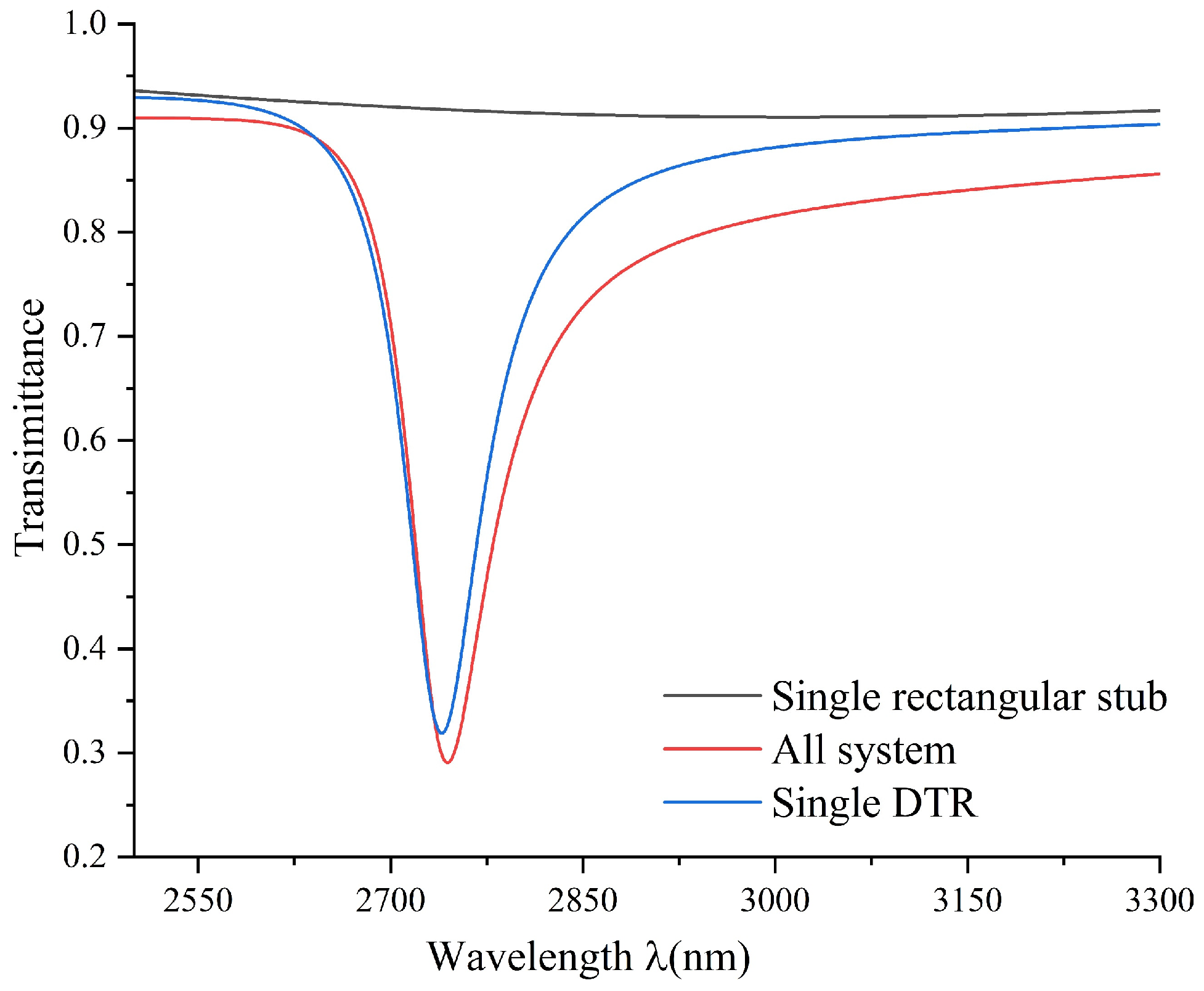
As depicted in
Figure 2, the black line, red line, and blue line, respectively, represent the transmission spectra of the single rectangular stub, all system, and the single DTR. The wavelength range was from 2500 nm to 3300 nm.
The transmission spectrum of a single rectangular stub had a slightly upward-sloping straight line, with light signals at most frequencies exhibiting high transmissivity, featuring continuous broadband transmission characteristics. Through transmission spectrum analysis, when the refractive index of the two structures was constant, the cavity corresponded to a very narrow range of wavelengths, manifesting as sharp peaks and presenting Fano resonance phenomenon.
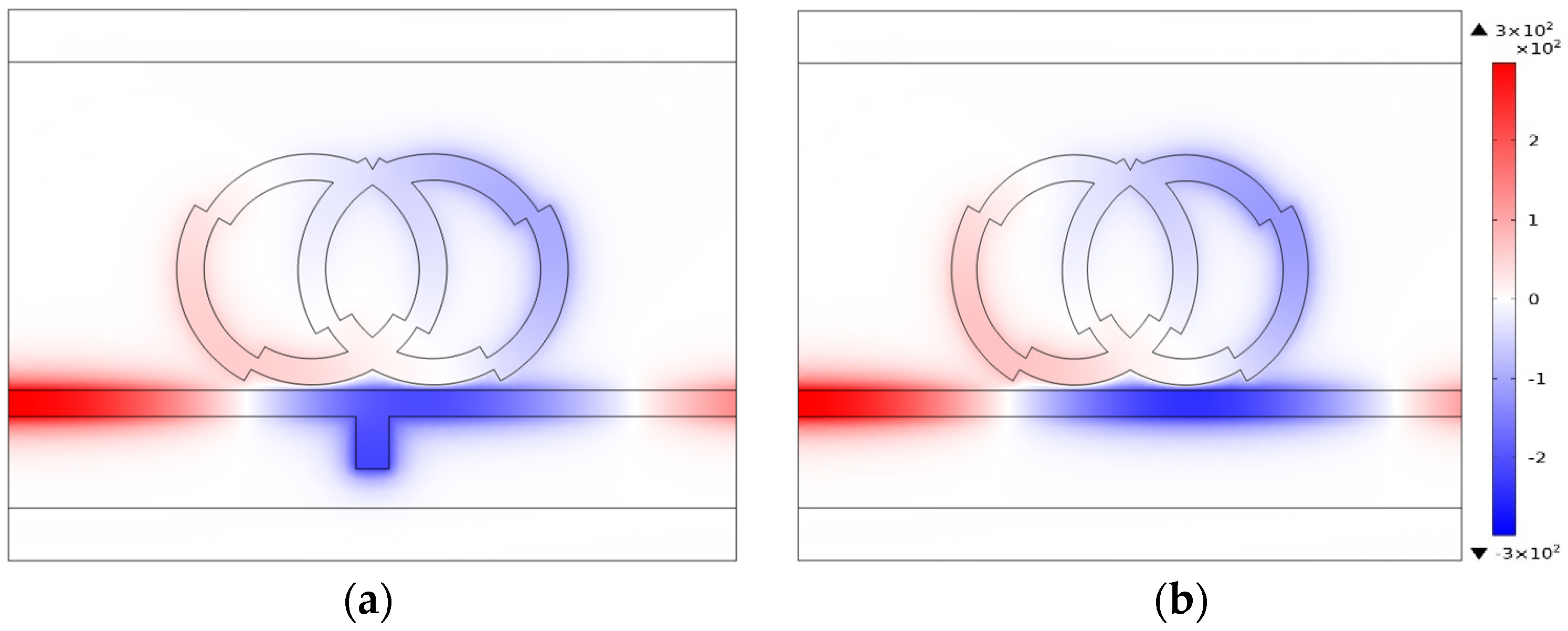
In order to better study the impact of the rectangular stub on Fano resonance, we investigated the sensing performance of an all system that consisted of the double-tooth ring structure with the rectangular stub, and the single TDR structure that did not couple the rectangular stub. As shown in
Figure 3, it can be observed that in both structures, SPPs can traverse the waveguide and couple into the cavity, undergoing significant resonance, and the magnetic field distributions were similar. Therefore, the introduction of the rectangular stub reduced the propagation of SPPs in the waveguide, generated stronger resonance, and promoted the occurrence of Fano resonance.
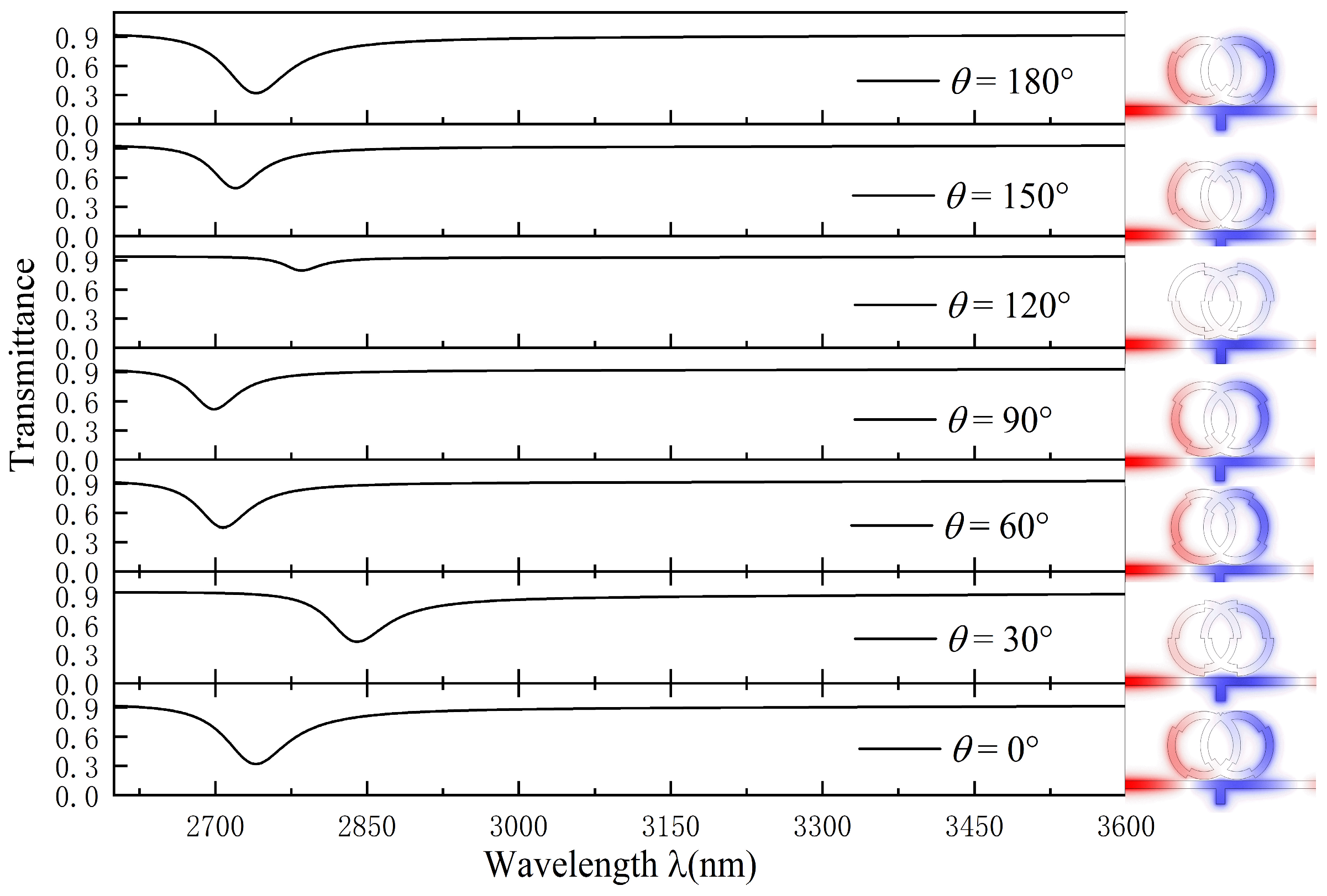
For the effect of different geometrical parameters on the nano refractive index sensor, the different angles of the TDR were first analyzed.
The initial structural parameters remained fixed. In order to study the effect of angle on the Fano resonance in depth, we compared the transmission spectra at different angles. The
θ values were set to 0°, 30°, 60°, 90°, 120°, 150°, and 180°. As shown in the transmission spectra in
Figure 4, the structure at
θ = 120° achieved a curve with high transmissivity, and the magnetic field strength of the coupled cavity was extremely low, indicating that this sensor had very poor light-limiting capability. When
θ = 0° (180°), the structure produced an ultra-low transmissivity, with an asymmetrical curve at larger wavelengths, demonstrating that Fano resonance exhibited high sensitivity. Meanwhile, from its transmission curve, it is known that
θ = 0° (180°) had a low trough, which had a better light-limiting ability.
As a nanoscale refractive index sensor, this property is very important to enable good stability during the detection process. The other angles produced transmission spectral lines, which all showed higher transmittance, inconsistent wavelengths, and poor propagation characteristics relative to those at 0° will not be analyzed one by one. In summary, the performance of the sensor varied significantly with the change in the rotation angle of the DTR. θ = 0° (180°) was the optimal rotation angle for the structure.
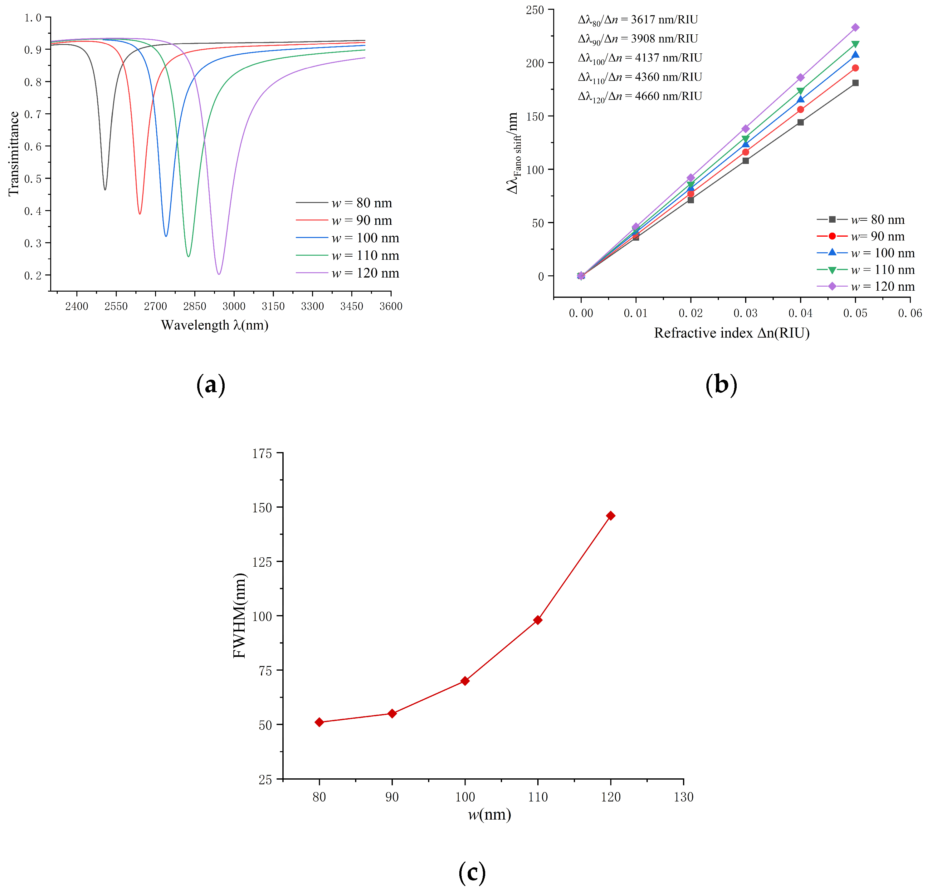
Subsequently, the impact of the width between the double-tooth rings on the sensor’s performance was studied. Keeping the initial structural parameters were unchanged, the
w was varied in steps of 10 nm, ranging from 80 nm to 120 nm. The results are shown in
Figure 5, from which it can be observed that as the width increases, the wavelength increases, and the waveform of the transmission spectrum shifts approximately equidistantly to the right; the FWHM width of the transmission curve of the transmission spectrum becomes larger. The sensitivity linear fitting for different slit widths is shown in
Figure 5b.
When the width increased, the overall system sensitivity increased. By calculating Figure of merit (FOM) using the formula, its FOM values were in the range of 70.9, 72.4, 59.1, 44.5, and 31.9; however, the structures of 80 nm and 90 nm were not selected for further discussion because highly optimized sensors may be more sensitive to changes in the environment or to rapid changes in the target substance, and the transmission curves have high troughs, which may result in shorter response times. In some applications, a long response time may be more appropriate, so we chose the w = 100 nm condition to achieve a longer response time.
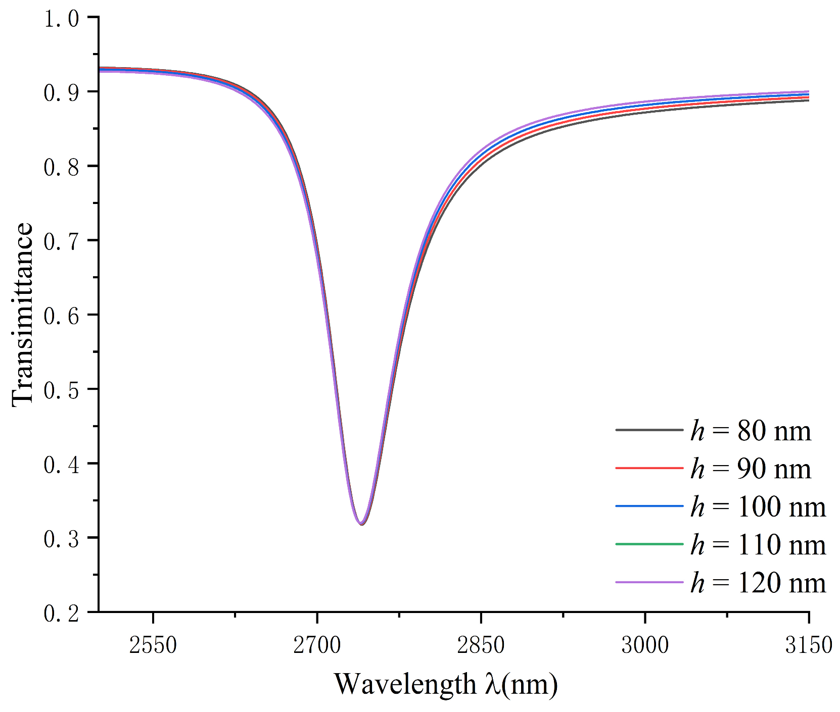
Based on the above discussion, we chose the width of 100 nm and the other geometric parameters remained invariant. Then, we examined the impact of the height of the rectangular stub in the coupled structure on the transmission characteristics. The height values of the rectangular stub were set to 80 nm, 90 nm, 100 nm, 110 nm, and 120 nm.
As shown in
Figure 6, the dip position of the Fano resonance remained basically constant as the height of the rectangular stub increased. The shape of the Fano resonance curve shows an asymmetric shape, and the degree of asymmetry gradually becomes larger.
In conclusion, in Fano resonance, the MIM waveguide has been designed by introducing a rectangular stub structure capable of triggering the resonance in the interface between the metal layer and the insulator layer. This structure results in the amplification and localization of propagating electromagnetic waves within a specific frequency range, giving the MIM waveguide a continuous broadband profile. The continuous broadband state affects the line profile (peak height and shape) of the Fano resonance, causing variations in the amplitude and shape of the propagating wave, but not on the wavelength of the dip (the wavelength of propagation in the waveguide).
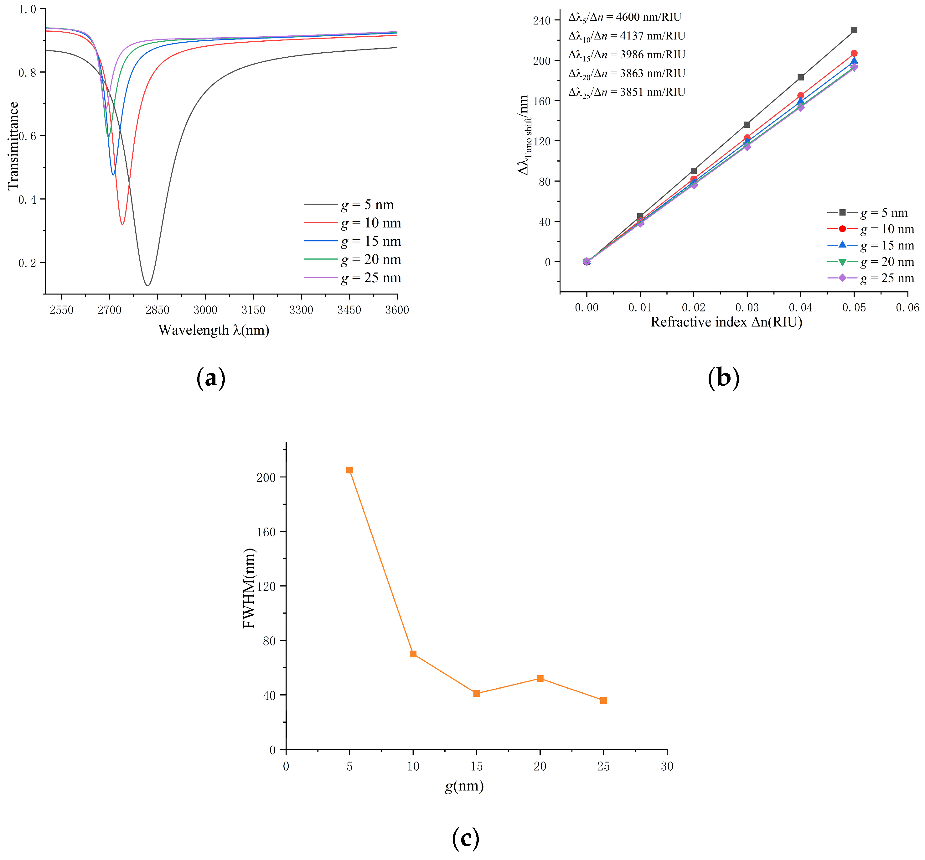
Following this, the impact of the coupling gap between the waveguide structure and the DTR structure on the sensing characteristics was assessed.
The initial structural parameters were unchanged, and the coupling gap varied within the range of 5 nm to 25 nm, with a step size of 5 nm. The transmission characteristics curves for different values are shown in
Figure 7. As the coupling gap got larger, the wavelength became smaller, resulting in a blue shift of the transmission wavelength; the FWHM decreased, the transmittance increased, the coupling strength weakened, and the resonance diminished.
The sensitivity decreased as the coupling gap increased. At g = 5 nm, the sensitivity reached 4600 nm/RIU, and at g = 25 nm, it was reduced to 3851 nm/RIU. When g < 10 nm, the FWHM line chart showed a very steep trend, resulting in a relatively small Figure of merit (FOM) value for the coupling structure at g = 5 nm. When g is less than or equal to zero, it effectively means that there is no gap, and the two structures are in direct contact. In this case, coupling effects can become very strong and may lead to highly non-linear behavior. This may include extremely large transmittances, very narrow FWHM, and highly sensitive sensing properties. So, the coupling gap at g = 10 nm was chosen to obtain the best sensing performance with low transmittance and at the same time the best sensing performance of the whole system.
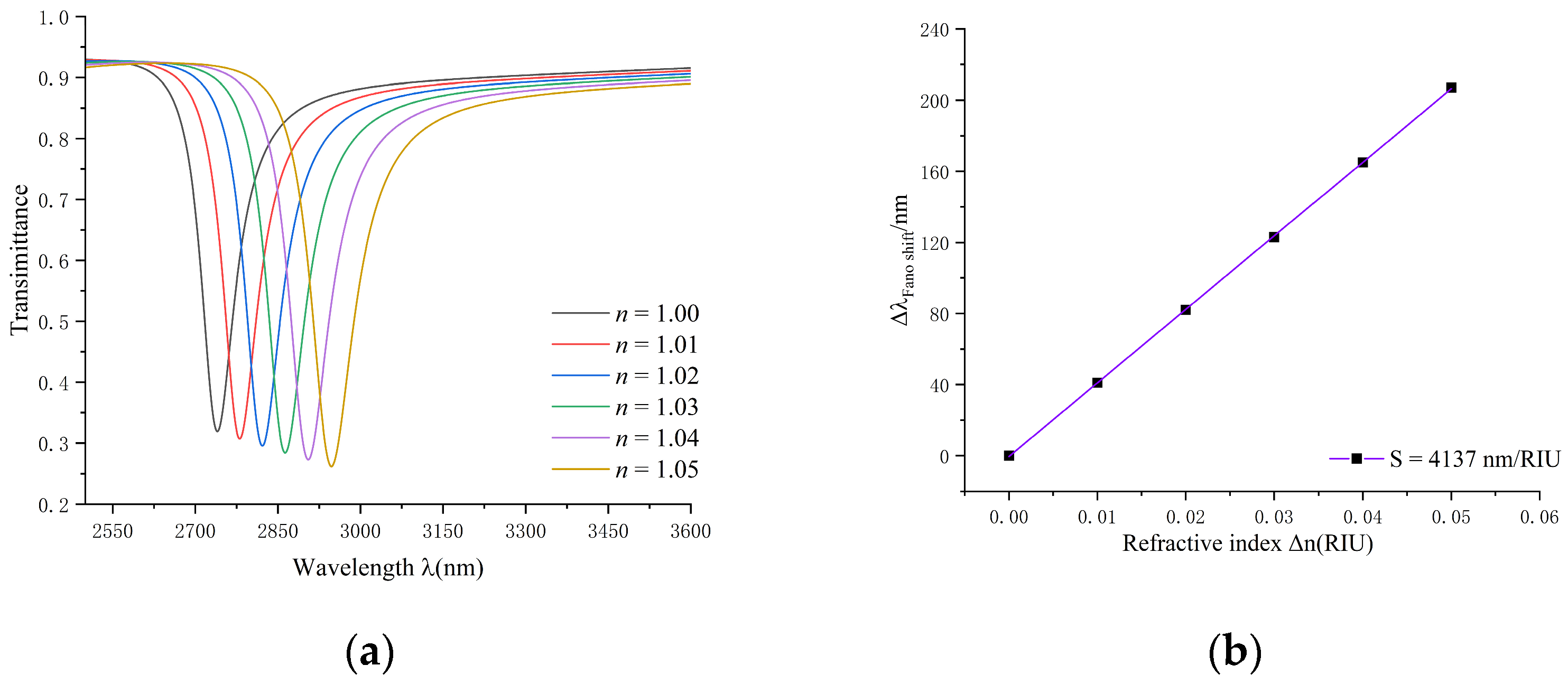
Finally, we analyzed the refractive index. The initial value of refractive index was
n = 1.00, the step size was 0.01, and ends when the refractive index was
n = 1.05. The results are shown in
Figure 8.
As the refractive index progressively increased, the corresponding wavelength also increased, leading to a noticeable redshift in the transmitted spectrum. The waveform of the transmission spectrum remained unaffected by changes in the refractive index. The wavelength differences between various peaks were the same, with wavelengths shifting equidistantly. Through linear fitting, the sensitivity of the DTR refractive index sensor was determined to be 4137 nm/RIU, with an optimal value of 59.1, representing the optimum parameters for this coupling structure (
Table 2).
To select the optimal performance index to ensure that the device can perform as expected, the effect of the refractive index change on the transmission spectrum must be carefully considered in the design of the optical device.
4. Application
Due to the sensing characteristics of the DTR structure, it exhibited high sensitivity, complex structure, and ease of miniaturization and integration. It is suitable for application as a sensor to detect oil concentration in industrial processes. The properties of oil–water mixtures depend on the ratio and physical properties of the oil and water. For example, during metal cutting and machining, machinery and equipment may become hot, and an oil–water mixture can serve as a coolant to help reduce the temperature of equipment and prevent overheating. The oil concentration in coolants typically ranges from 5% to 20%. In addition, oil–water mixtures in detergents can be used to remove oil stains, usually at a concentration of 0.1% to 5%. Oil concentrations in food processing can vary from 10% to 100% depending on the type of food and cooking method, and so on.
The mixture refers to oil and water mixed in different proportions and then turned into other solvents through a special process. Such solvents because of the different oil content (water content), will produce a change in the refractive index. In filling to the nano-refractive index sensor, it will be because of the difference of refractive index, which will cause the change of wavelength.
The process of monitoring the oil concentration using this sensor is shown below: the oil–water mixture is used to exhaust the air from the recesses of the sensor. When the nanosensor comes into contact with the oil–water mixture, the air in the groove is expelled, filling the groove with liquid. Since the oil–water mixture has a different concentration, the corresponding refractive index is also different. By monitoring the transmission or reflection of light, the nanosensor generates an image called a Fano resonance curve. As the oil concentration changes, the refractive index of the medium of the oil–water mixture also changes, which can lead to changes in the Fano resonance curve. The nanosensor detects these changes and compares them to a pre-established oil concentration–refractive index relationship.
The relationship between oil concentration and refractive index was found as follows:
where
is the refractive index of the oil–water mixture,
is the refractive index of the water,
is a constant related to the composition and wavelength of the mixture, and
is the concentration of the oil in the mixture.
Monitoring of the oil concentration was carried out at 20 °C with a constant k of 0.04 and of 1.333. The oil concentration was taken as 0%, 20%, 40%, 60%, 80%, and 100%. The refractive index of the oil–water mixture was calculated as 1.333, 1.339, 1.345, 1.351, 1.357, and 1.363.
The sensitivity
of the concentration sensor can be given by the following equation:
In this equation, represents the translation of the transmission spectrum and represents the concentration change.
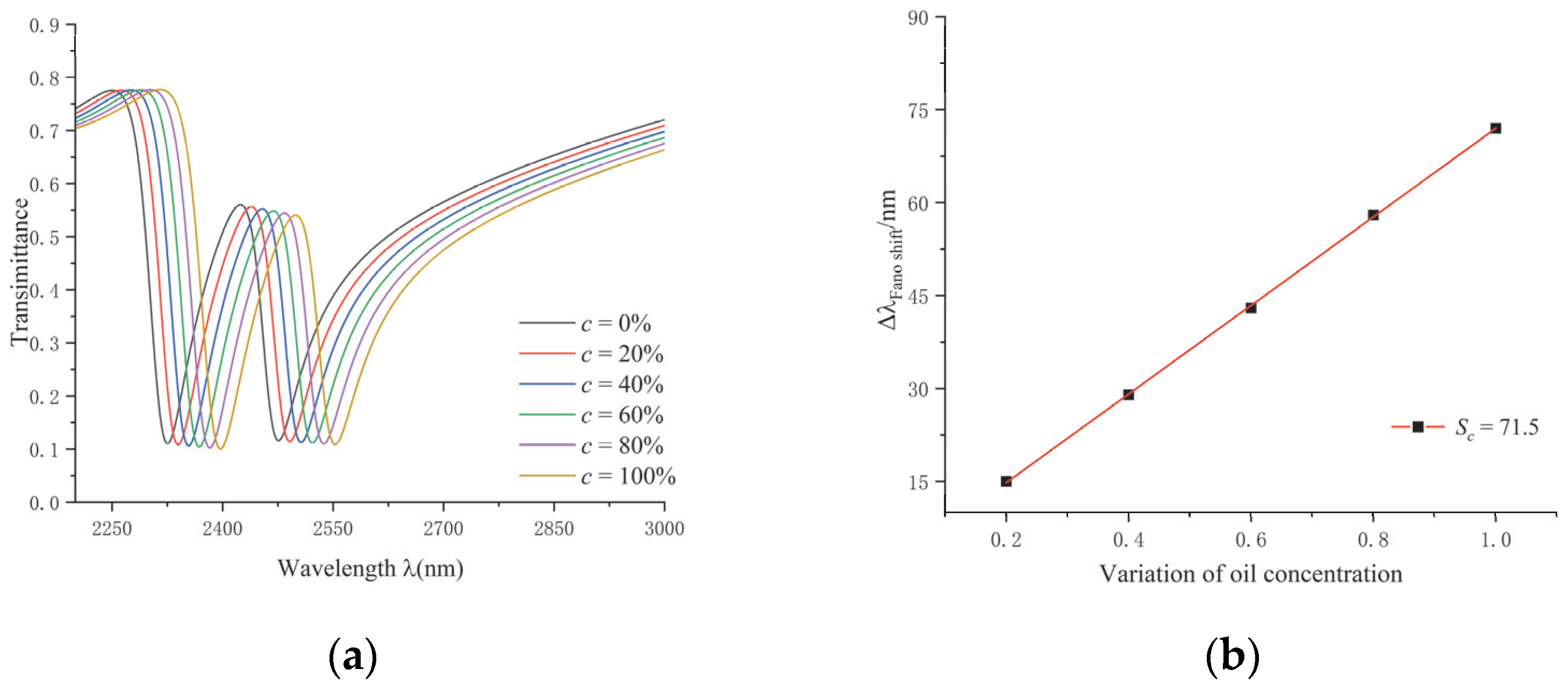
The transmission curve and sensitivity are shown in
Figure 9. The transmittance of the sensor was too large in the second trough, so it was analyzed with the first wave trough. As the concentration of the oil became larger, the position of the trough moved from 2325 nm to 2397 nm, the curve shifted approximately equidistant to the right, and the transmittance curve showed an obvious red shift. Modern optical instruments can be accurate down to the nanometer scale and can accurately detect wavelengths. The linear fit line for the sensitivity of the sensor is shown in
Figure 9b, and the sensitivity of the concentration sensor was calculated to be 71.5 in order to ensure the accuracy of the measurement.


 ,
, 


