Article

Concurrent Thermal Reduction and Boron-Doped Graphene Oxide by Metal–Organic Chemical Vapor Deposition for Ultraviolet Sensing Application

1
School of Semiconductor and Chemical Engineering, Semiconductor Physics Research Center, Jeonbuk National University, Jeonju 54896, Republic of Korea
2
VKTECH Research Center, Nguyen Tat Thanh University, Ho Chi Minh City 70000, Vietnam
3
LED Agri-Bio Fusion Technology Research Center, Jeonbuk National University, Iksan 54596, Republic of Korea
*
Authors to whom correspondence should be addressed.
These authors contributed equally to this work.
Appl. Nano 2024, 5(1), 1-13; https://doi.org/10.3390/applnano5010001
Submission received: 24 October 2023 / Revised: 5 December 2023 / Accepted: 12 December 2023 / Published: 28 December 2023
(This article belongs to the Collection Feature Papers for Applied Nano)

Abstract

:
We synthesized a boron-doped reduced graphene oxide (BrGO) material characterized by various electrical properties, through simultaneous thermal reduction and doping procedures, using a metal–organic chemical vapor deposition technique. X-ray photoelectron spectroscopy (XPS) was used to study the impact of the doping level on the B bonding in the reduced graphene oxide (rGO) layer that is influenced by the annealing temperature. The synthesized BrGO layer demonstrated a high B concentration with a considerable number of O-B bonds, that were altered by annealing temperatures. This resulted in a decreased work function and the formation of a Schottky contact between the BrGO and n-type Si substrate. Due to the higher proportion of B-C and B-C3 bonding in the BrGO/Si device than that in the rGO/Si, the decreased Schottky barrier height of the BrGO/n-Si vertical junction photodetector resulted in a higher responsivity. This study showcases a promise of a simple B-doping method in use to alter the electrical characteristics of graphene materials.

1. Introduction

In recent years, many studies have focused on the various methods of forming graphene oxide (GO) materials to enhance their electrical properties by adjusting the functionalization with metal, metal oxide, or interstitial/substitutional doping with heteroatoms, such as nitrogen (N), phosphorous (P), boron (B), or antimicrobial peptides [1,2,3,4,5,6]. By applying a specific temperature, plasma treatment, electric field, and heteroatom dopant, GO can be transformed from an insulator into an n- or p-type semiconductor [7,8,9].
Our group has successfully achieved N- and Ga-doped reduced graphene oxide (rGO) through a metal–organic chemical vapor deposition (MOCVD) system using NH3 gas and a triethylgallium (TEGa) as the N and Ga source, respectively [10,11]. The N-doped rGO materials were obtained using different doping levels with varying NH3 flow rates at identical annealing temperatures in the MOCVD system. The doping pulse mode was used to control the dopant composition of the Ga-doped rGO. The system efficiently produced doped rGO using various variables, such as the dopant source types, dopant source volumes/rates, and annealing temperatures. Temperature was found to have a significant effect on the doped materials’ electrical properties. Among the various heteroatom-doped graphene materials, B-doped rGO (BrGO) has rarely been investigated for their responses to different annealing temperatures in MOCVD system at identical dopant sources.
Lv et al. synthesized boron-doped graphene (BG) using bubbler-assisted chemical vapor deposition (CVD) and the resulting BG sheets demonstrated enhanced sensitivity when detecting toxic gases, such as NO2 and NH3 [12]. Furthermore, several research groups have reported chemically synthesized methods for B-doped rGO in aqueous solutions, such as boric acid or boron oxide [6,13,14,15]. Yeam et al. reported that high concentrations of B atoms in BrGO annealed at high annealing temperatures increased the carrier concentrations, resulting in an improved specific capacitance [7]. According to Sahoo et al., the SnO2/BG anode in a Li-ion battery exhibited enhanced stability over cycles and improved reversible capacity due to the increased B doping [13]. Prior studies concerning BrGO properties have frequently been conducted in a powder or solution form [13,14,15,16]. However, these forms’ processes are inappropriate for large-scale processing when using BrGO in optoelectronic devices. To address this issue, we introduced a technique for manufacturing wafer-scale BrGO materials using the MOCVD system, with triethyl boron (TEB) as the metal–organic B precursor. This technology offers significant potential for the application of BrGO materials in optoelectronic devices.
Ultraviolet (UV) photodetectors utilize chemically stable and highly resistant materials with a large energy bandgap, such as GaN, SiC, AlGaN, and ZnO [17,18,19,20,21]. Unfortunately, the comparatively low-quality epitaxial layer of these materials limits their potential for high-speed UV sensing as it causes the slow recovery of the photocurrent. Si photodetectors have a high-speed detection capacity but function poorly in UV due to a high reflection coefficient and a low UV light penetration into the material. Si–Schottky junctions may be required for enhancing the surface layer with large absorption or reflection while enabling effective separation and rapid charge collection. The formation of Si–Schottky junctions with Ag nanowires, PtSe2, graphene, rGO, and metal nanoparticles has been shown to effectively decrease surface recombination [22,23,24,25,26].
Many studies have employed graphene- and rGO-based materials as active materials for photodetection [27,28,29,30]. Chitara et al. demonstrated the rGO photoresponse in UV (at 360 nm) and infrared (IR) (at 1550 nm) regions, and the photodetection responsivity was 0.12 A/W and 4 mA/W with external quantum efficiencies of 40% and 0.3%, respectively [16,27,28]. Lai et al. reported that two rGO-based photodetector devices annealed at two different temperatures demonstrated a broadband photoresponse from 290 nm to 1610 nm, covering UV to IR [29]. The device showed less responsivity and a longer response time in the near-IR region than in the UV-to-visible regions. Li et al. demonstrated that the rGO/n-Si p-n vertical heterojunction structure with a Schottky contact displayed a high photoresponsivity and fast response toward UV–near-IR light with zero power consumption [26].
We characterized the electrical properties of BrGO at various annealing temperatures with respect to simultaneous thermal reduction and doping processes via the MOCVD system. The B-bonding level of the BrGO layer was determined using X-ray photoelectron spectroscopy (XPS) based on the B1s and O1s peaks. The relationship between the doping level of the BrGO layer and the device properties led to the discovery of the reliance of BrGO layers on doping levels in n-type Si/BrGO Schottky diodes.

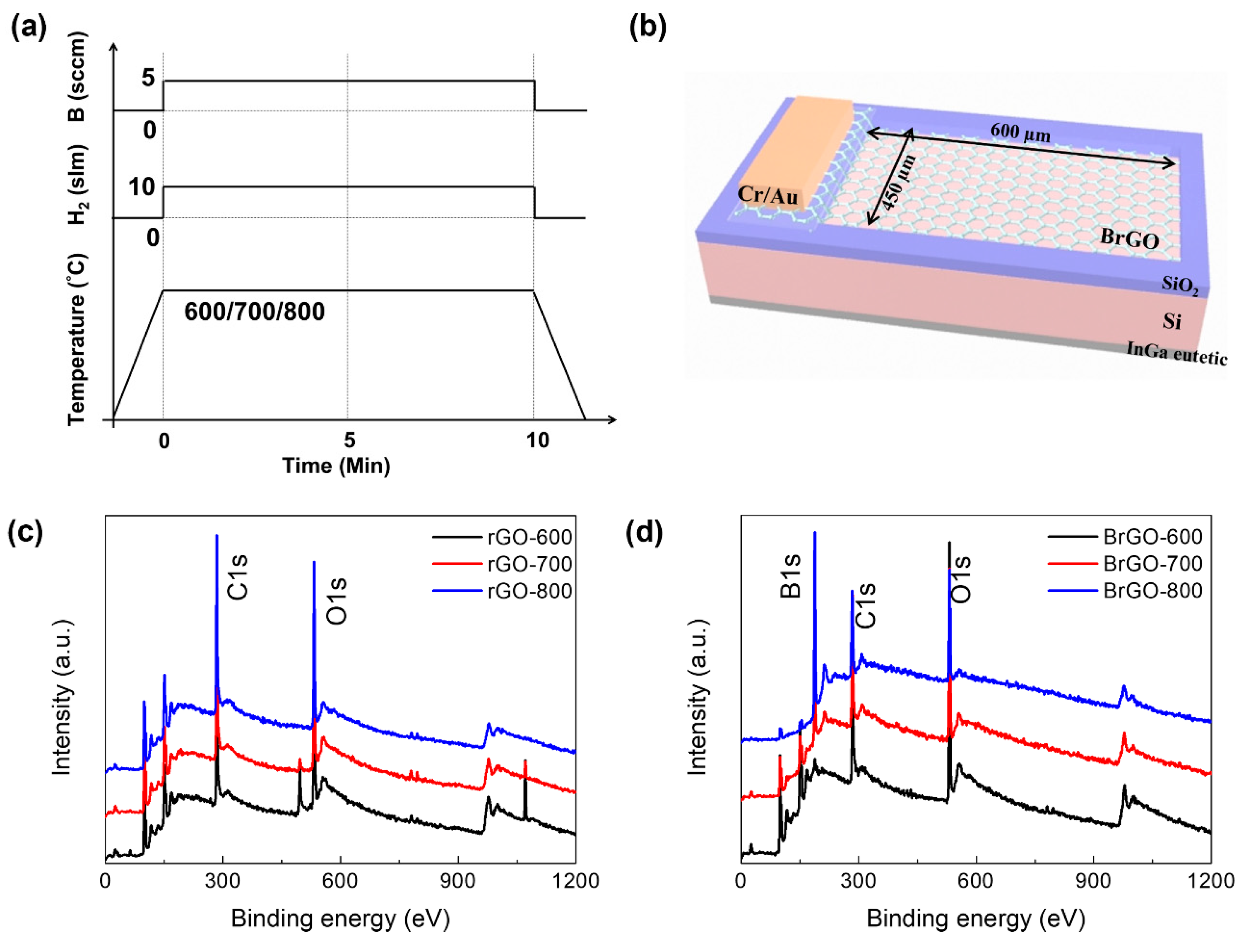
2. Materials and Methods
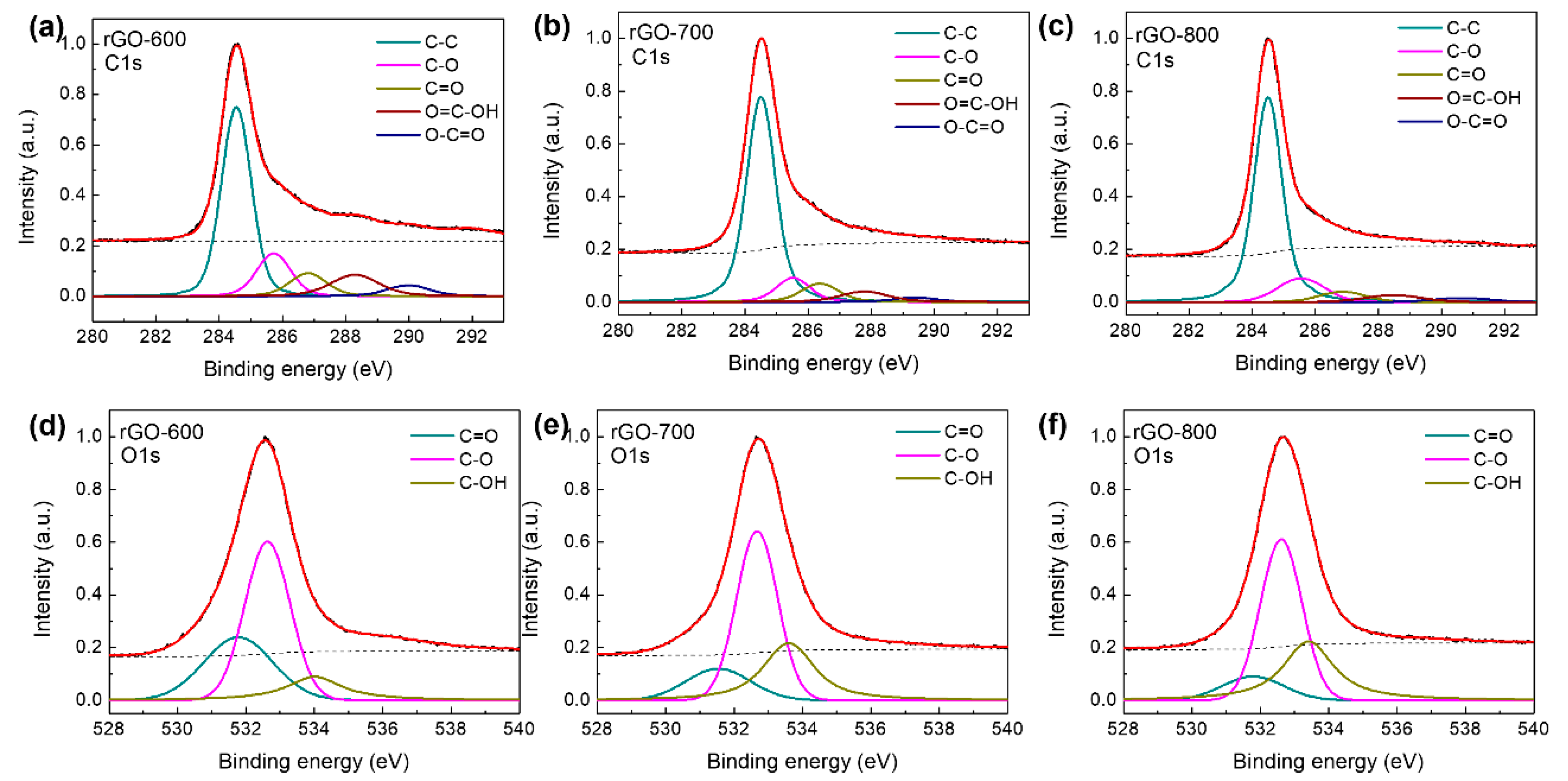
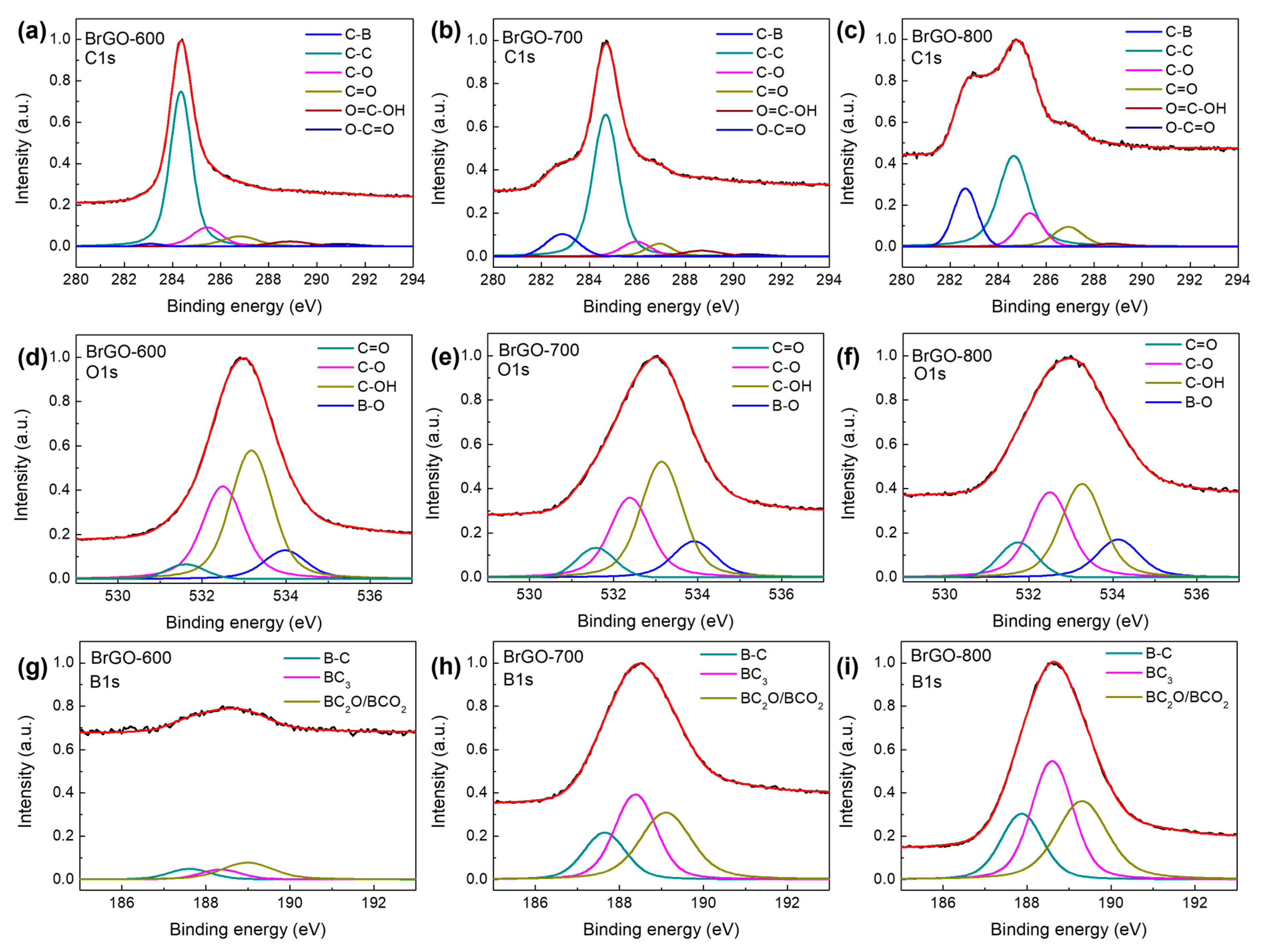
The synthesis of a 0.5 g/L GO solution using the modified Hummer method was described in a previous work [11]. The prepared uniform GO layer was spray-coated onto a cleaned 450 µm thick n-type Si substrate. The thickness of the GO layer (20 nm) was measured by atomic force microscopy (AFM) [11]. To produce the rGO layer, the as-prepared GO layers were annealed in hydrogen ambient for 10 min inside the MOCVD system at 600, 700, and 800 °C, respectively. The rGO layers were thinner (~10 nm) than the GO layers because annealing eliminated the oxygen functional groups. The BrGO layer was made using the TEB precursor (B(C2H5)3, SAFC Hitech Ltd., Kaohsiung, Taiwan) as a dopant, injected at a rate of 5 sccm. The effect of annealing temperatures on the doping level of the BrGO layers was investigated, as denoted by BrGO-600, BrGO-700, and BrGO-800, respectively. Figure 1a shows the MOCVD doping and annealing processes. Using an ultrahigh vacuum chamber (0.933 kPa) and an Al Kα radiation source (1486.8 eV), chemical bonding was analyzed using XPS (AXIS-Nova, Kratos, Kyoto, Japan). With the incidental carbon C1s peak at 284.8 eV serving as a reference, the binding energy values of XPS spectra were determined. Utilizing a He I ultraviolet source (hυ = 21.2 eV), ultraviolet photoelectron spectroscopy (UPS, AXIS-Nova, Kyoto, Japan) was used to measure the work function. Using gold as a reference and an applied bias voltage of −15 V, the work function value was measured from the secondary-electron cut-off. X-ray diffractograms (XRD) were obtained using a Cu Kα incident beam (λ = 0.1541 nm) operated at 40 KV and 15 mA, monochromated by a nickel filter. For XPS, UPS, and XRD analysis, the samples were prepared by rGO or BrGO onto a precleaned Si substrate. The optical absorption was measured using a JASCO V-570 UV-visible-NIR spectrophotometer (JASCO, Easton, MD, USA).
For the characterization of the n-Si-based photodetector devices, a 300 nm thick SiO2 layer on the n-Si substrate was shaped into a 600 µm × 450 µm rectangle using photolithography and treated with buffered oxide etch solution to bond the metal. The rGO or BrGO layers were added to the SiO2/n-Si substrate using the spray-coating and MOCVD doping methods. The active area of the photodetector devices (approximately 650 µm × 600 µm) was defined using photolithography and an oxygen-plasma etching by an inductively coupled plasma-reactive ion system. Subsequently, Cr/Au (20/150 nm) was deposited on the front rGO or BrGO electrode on the patterned SiO2 layer by electron beam deposition. The device structure is shown in Figure 1b. In-Ga eutectic paste in contact with a Cu foil was used for the rear electrode. The current-voltage (I–V) characteristics were evaluated with a semiconductor analysis system (Keithley 4200-MS tech, Hawseong, Republic of Korea) under exposure of a 385 nm UV LED. The responsivity spectrum was measured by an Oriel Cornerstone 130 1/8 m monochromator as a light source and a Xenon lamp (450 W).

3. Results

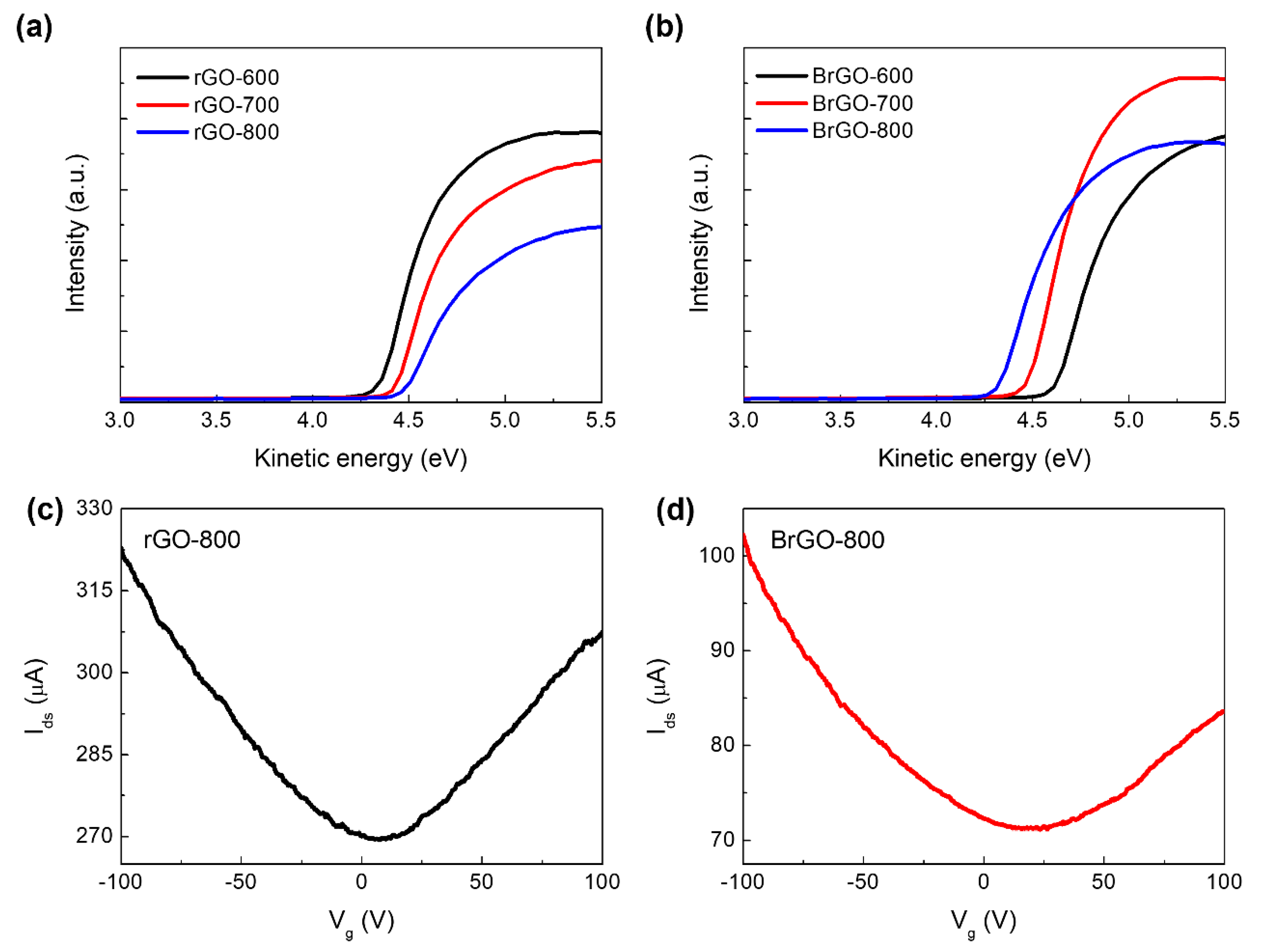
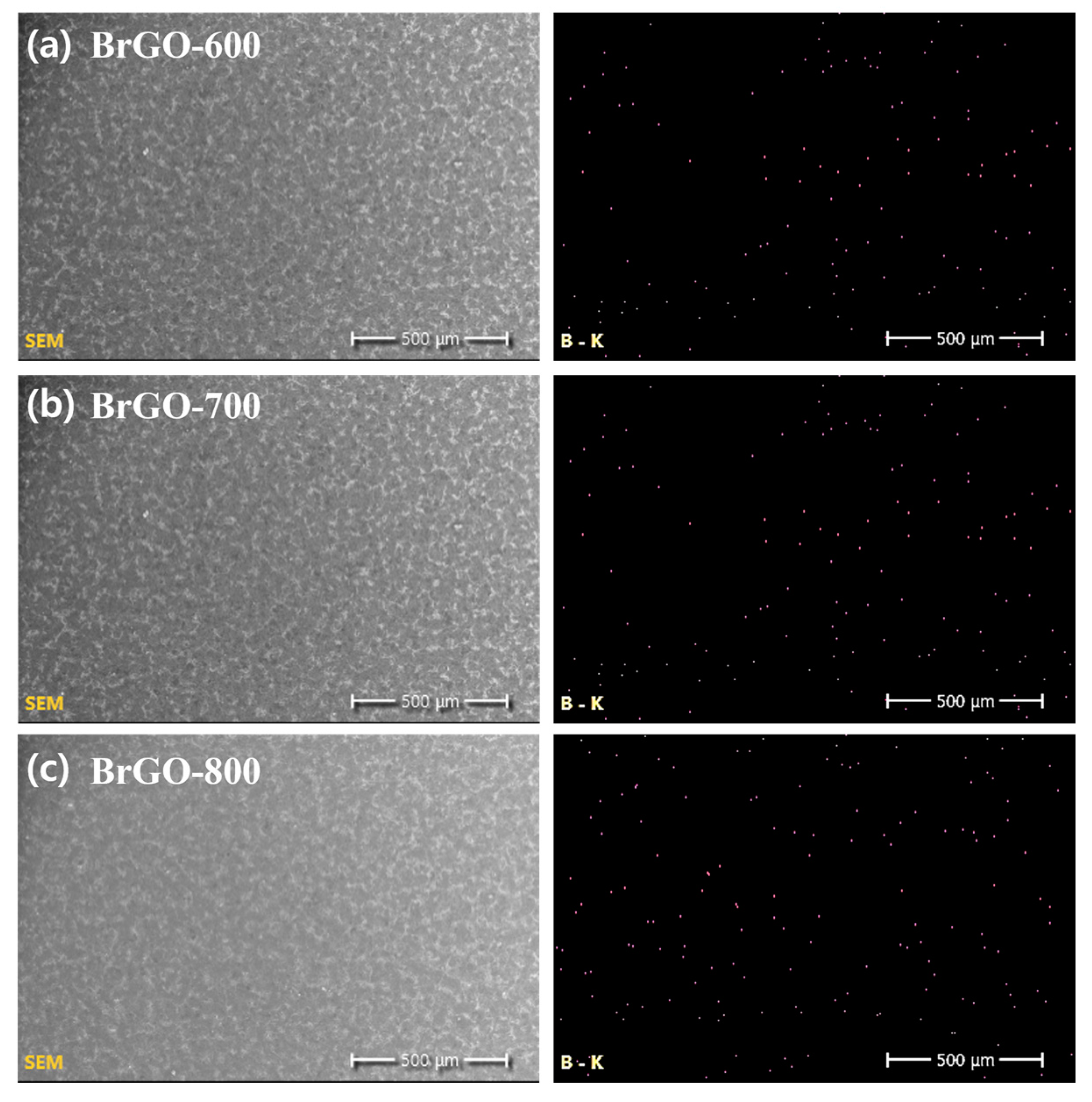
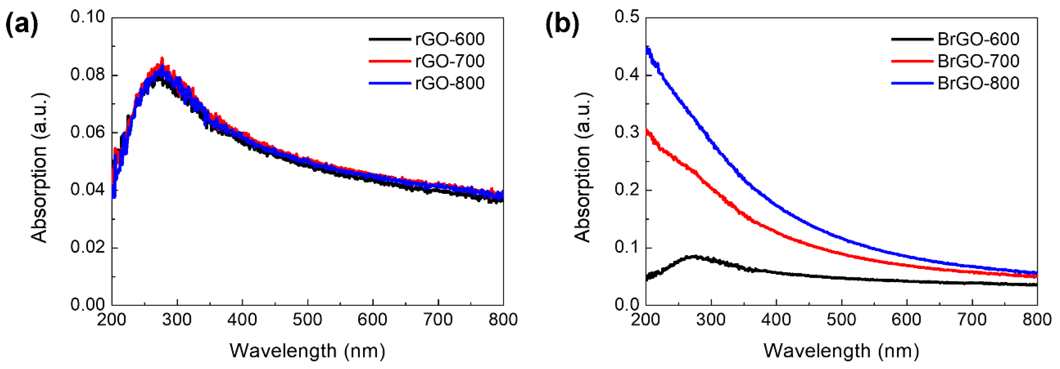
3.1. Impact of Annealing Temperature

Figure 1c,d depict the XPS spectra of rGO and BrGO annealed at different temperatures, illustrating the role of the B dopant during the thermal reduction of rGO in the MOCVD system. The successful doping of B atoms in the rGO crystalline network is demonstrated by the emergence of the B1s peak in the BrGO XPS spectra. The peaks at 284, 530, and 180 eV on wide-scan spectra correspond to carbon (C), oxygen (O), and B atoms. B atoms comprise 0.79%, 2.43%, and 4.52% of the BrGO samples annealed at 600 °C, 700 °C, and 800 °C, respectively. To learn more about the chemical configuration of the C, O, and B atoms in the XPS spectra, these peaks were deconvoluted and are displayed in Figure 2 and Figure 3. Every fitting parameter was adjusted according to the literature. The XPS C1s spectra of rGO consisted of five types of components: C–C (284.6 eV), C–O, or C–OH (285.6 eV), C=O (287.2 eV), O=C–OH (288.9 eV), and O–C=O (291.2 eV), as shown in Figure 2a–c [13]. The C/O ratio of the rGO samples was ~1.58 (rGO-600), 2.25 (rGO-700), and 2.98 (rGO-800), respectively. Figure 2d,e show that the O1s peak can be fitted into three peaks corresponding to O=C (531.5 eV), O–C (532.6 eV), and C–OH (533.6 eV), respectively [13]. The proportion of C=O bonds decreased as the annealing temperature increased. The BrGO samples displayed an additional peak at 282.8 eV, indicating C–B bonds due to the B-doping, as shown in Figure 3a–c [31,32,33]. Agnoli et al. reported that B-doped graphene material includes various functional groups ranging from substitutional B to boronic (C=B–OH) and borinic (C–B=OH) esters and organo-borane (C–B–H) according to the Ball model of BG [34]. The B/C and O/C area ratios in the XPS C1s peak were 0.02 and 0.37 for BrGO-600, 0.16 and 0.29 for BrGO-700, and 0.35 and 0.36 for BrGO-800, respectively. The annealing temperature increased with the reduction of the oxygen functional groups in rGO; however, the XPS C1s spectra of both BrGO-700 and BrGO-800 samples show an oxygen bonding portion with a high annealing temperature due to an increase in both boronic and borinic bonds. The XPS O1s spectra showed four-component peaks corresponding to C=O (531.6 eV), C–O (532.4 eV), C–OH (533.2 eV), and B–O (533.9 eV), as shown in Figure 3d–f [33,35]. The existence of B–O bonds in the BrGO-600 layer indicated that there were B-doped rGO domains within the BrGO. The BrGO-800 layer has a lower C-OH bonding component, which caused an increase in both boronic and borinic bonds compared to the BrGO-700 layer. The deconvolution of the XPS B1s spectra at 187.6, 188.3, and 189.1 eV revealed the B–B, B–C, and B–O bonds, as shown in Figure 3g–i [36,37]. The intensity of XPS B1s peak enhances with increased annealing temperature; the B–C bonding in the BrGO layer means that the substitutional B dopant is attached to the rGO layer. The XPS spectra showed that the BrGO layer was formed using the MOCVD system under the aforementioned annealing temperature conditions.
The ability of modify the work function of rGO materials is highly anticipated because this electrical parameter crucially affects optoelectronic device performance. The synthesis and reduction methods used, which typically result in varying aromatic sizes, degree of defect, and number of functionalized groups on the rGO layers, cause a significant change in the work function value [11]. We investigated the effect of the B dopant and the annealing temperature on the tunability of the work function value. Figure 4a,b show the effect of the B atom as well as the annealing temperature on the BrGO layer, as determined by UPS. The work function (Φ) was expected from the empirical relation shown in Equation (1):
Φ = hυ − (EF − Ecutoff)
where hυ, EF, and Ecutoff are the photon energy of the incidental light (21.22 eV), the Fermi level edge, and the measured secondary electron cutoff or inelastic low-kinetic-energy cutoff, respectively [11]. The Ecutoff and EF values are obtained from the UPS spectra. The work function values of the rGO samples were 4.84 (rGO-600), 4.24 (rGO-700), and 4.14 eV (rGO-800). The value of the work function decreased as the annealing temperature increased, since the higher the annealing temperature, the more oxygen functional groups are removed [29]. The work function values of BrGO samples were 5.12 (BrGO-600), 4.95 (BrGO-700), and 4.88 eV (BrGO-800). Previous studies have reported that heteroatom-doped rGO has a higher work function value than the rGO, and the work function value is dependent on the doping concentration [11]. These findings suggest that the B atoms were doped into rGO layers to form a BrGO layer and that the work function of the BrGO sample depends on the B atom concentration.
Electrical transport evaluations of rGO-800 and BrGO-800 were conducted in a vacuum to reveal the doping effect. As stated when describing device fabrication, the rGO (with and without B-doping) field-effect transistor (FET) devices were manufactured with a back gate on 300 nm thick SiO2/Si substrates with 30/100 nm Cr/Au pads [11]. The rGO layer acts as a channel with a length of 20 µm and a width of 350 µm. The I-V characteristics were measured in a vacuum at approximately 1 × 10⁻⁴ kPa. The drain-source current (Ids) versus gate voltage (Vg) and the typical characteristics of rGO back-gate FETs are displayed in Figure 4c,d. The rGO FETs exhibit p-type behavior because the Dirac point (VDirac), which is the minimum Ids value, showed a positive voltage [11]. The VDirac is approximately 8 V for rGO-800 and 23 V for BrGO-800, which implies p-type behavior. The Dirac point shift suggests that B-doping reflects p-type doping properties. There is an energy band gap with a Fermi level that is lower than the Dirac level due to the presence of the B atom. This means that a dipole moment was produced on the surface of the rGO layer by the dopant [38]. Based on the XPS results, we hypothesize that the oxygen atoms bonded to the B atoms prompted the doping-induced shifts in the Dirac point. We considered both BrGO-600 and BrGO-700 layers to verify the p-type characteristics (results not shown). Consequently, we believe that GO can be concurrently reduced to form rGO and doped with B using MOCVD, making it feasible to manufacture wafer-scale graphene-based optoelectronic devices.
The presence of B atoms in the rGO layer was confirmed by energy-dispersive X-ray spectroscopy (EDS) mapping of scanning electron microscopy (SEM) images, as shown in Figure 5. The BrGO layers showed the folding/wrinkle on surface owing to the spray-coated BrGO method. The surface layers’ red color is from the B atoms within B-K emissions. As a result, we believe B atoms were present in the rGO layer.
Figure 6 displays the UV-Vis absorption spectra of rGO and BrGO at different annealing temperatures. Generally, GO exhibits a peak at approximately 200 nm, which corresponds to the π-π* transition of the sp2 C–C bond. The peak of the rGO layer at different annealing temperatures shows a clear red shift of approximately 270 nm. The red shift is explained by the increase in sp2 content within the rGO caused by annealing [29]. Despite their different annealing processes, all the rGO layers have similar peak positions and absorption values. The BrGO samples showed an absorption peak of approximately 270 nm, which corresponds to the restoration of electronic conjugation on reduction, similar to the rGO layers annealed at different temperatures. However, the BrGO absorption values are higher than those of rGO [1,39]. The BrGO-800 sample did not show a peak because of the linear absorption spectra and B dopant atoms that suppress light absorption. Yang et al. reported that an increase in the doping level reduces red shift because doped free carriers enhance screening and consequently reduce electron–hole interactions [40]. The n to π* transitions in the C=B or C–B and C=O bonds may be connected to substitutional B doping levels, which could be the cause of the linear absorption spectra in BrGO. This indicates the heterogeneous distribution of B atoms in the carbon network of the rGO sheets and correlates to the electron transfer from B states to the π* states [41]. The absorption spectra of BrGO in the UV region (200–400nm) seem to have depended on the increased annealing temperature. There was a consistent decrease in light absorption from 400 nm to 800 nm, which is attributed to the minimization of sp2 C–C domains in the BrGO sheets. This implies that BrGO synthesized at a high annealing temperature can function as the active layer of a photodetector device in the UV region.

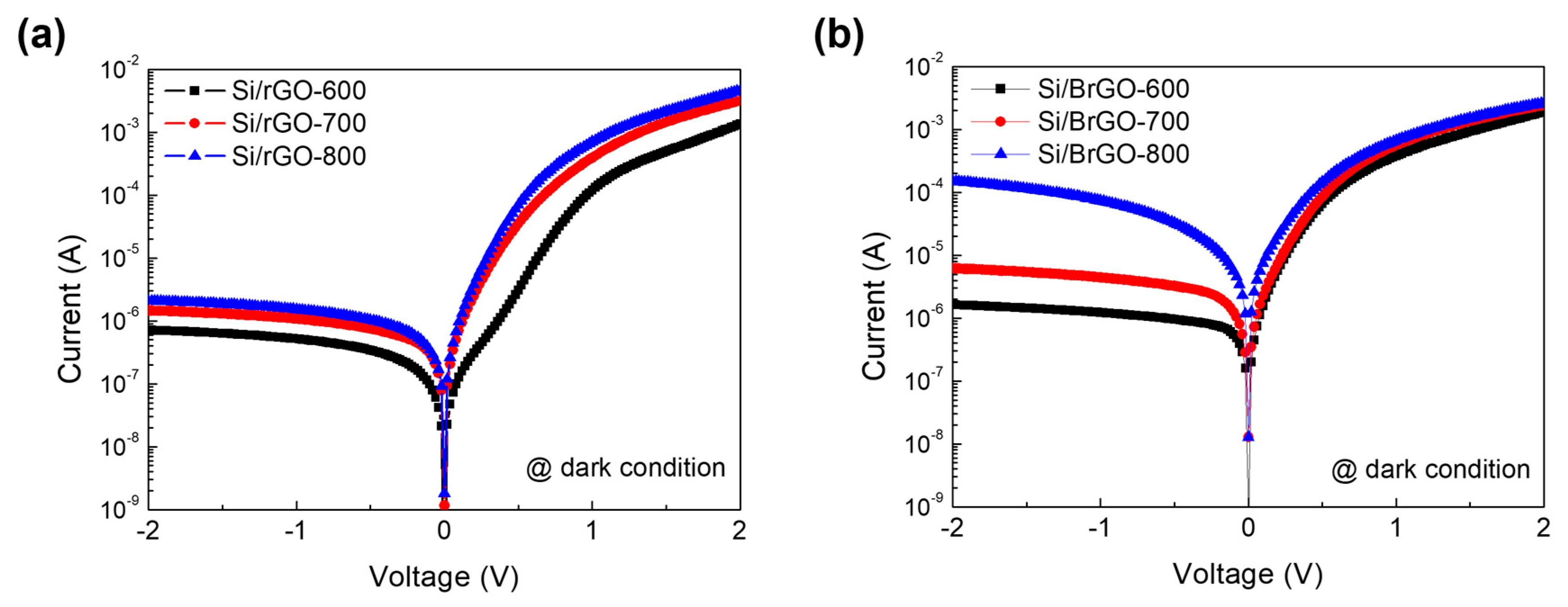
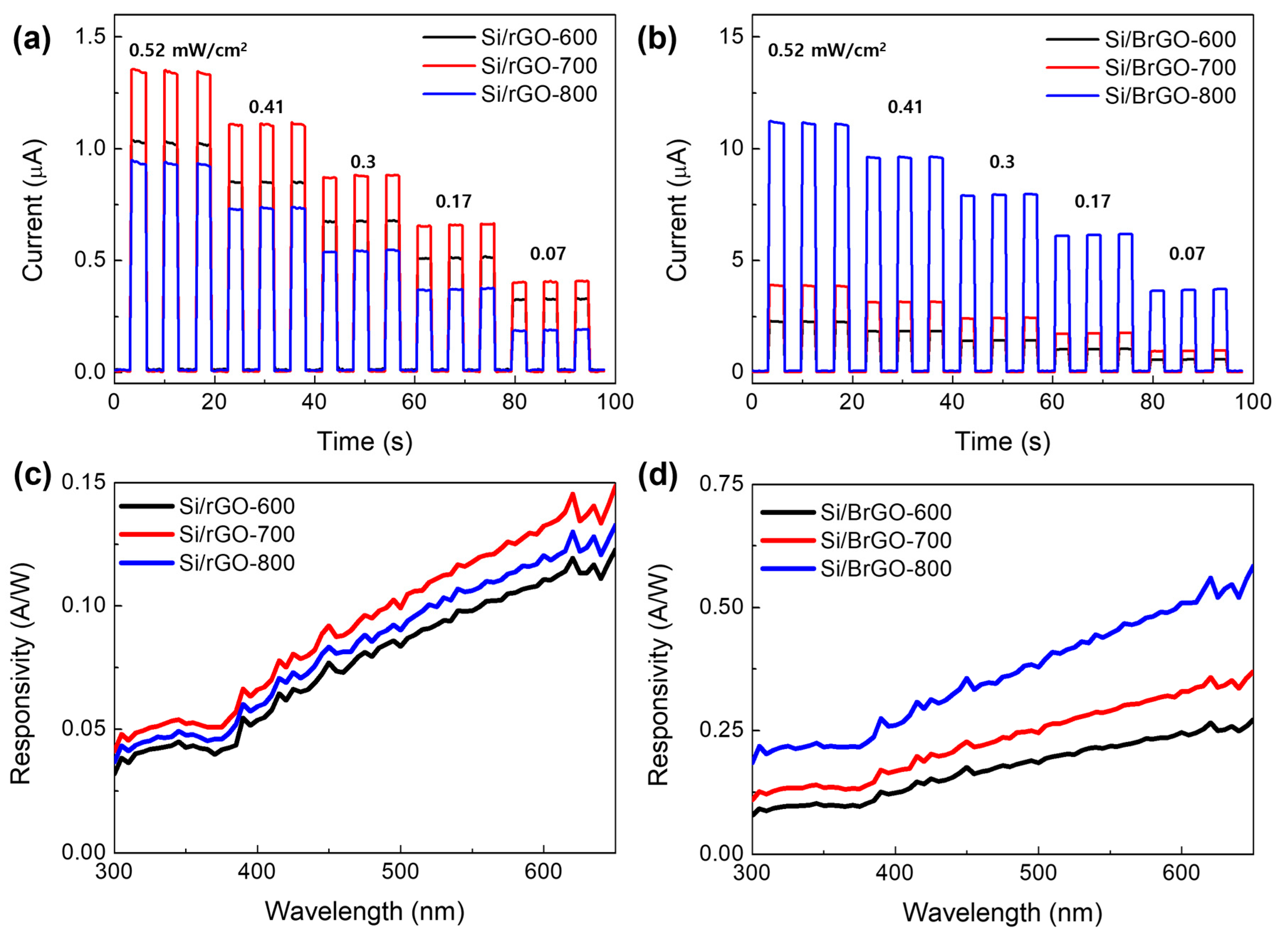
3.2. Electrical Characterization of BrGO/n-Si

Figure 7 shows the electrical properties of the rGO and BrGO layers on n-type Si devices annealed at different temperatures under dark conditions. The semi-logarithmic I–V curves of the rGO/Si and BrGO/Si diodes show Schottky behavior. The diode characteristic of the Schottky junction is described using the thermionic emission (TE) theory from dark I–V curves to verify related parameters such as the Schottky barrier height and work function as follows:
I = Is [exp(eV⁄nkT) − 1]
and:
Is = AA* T2 exp((−eΦSBH)/kT)
where Is, e, n, k, T, A, ΦSBH, and A* is the saturation current, the electronic charge, the ideality factor, the Boltzmann constant, the absolute temperature, the active area, the Schottky barrier height, and the Richardson constant of Si (~112 Acm−2K−2), respectively. Using TE theory, the Schottky barrier height of the rGO-600, rGO-700, and rGO-800 were calculated to be 0.73, 0.70, and 0.69 eV, respectively. The BrGO/Si devices also display the Schottky junction; however, the BrGO/Si device forms an ohmic junction at high annealing temperatures (over 900 °C). The calculated Schottky barrier height of Schottky devices was 0.68 eV for BrGO-600/Si, 0.66 eV for BrGO-700/Si, and 0.63 eV for BrGO-800/Si. These findings indicate that, when the doping concentration increases, the BrGO-800/Si junction of the Schottky barrier height is lower and the built-in electric field in the junction becomes weaker. This allowed us to predict the work function, which is the variation in value between the Schottky barrier height of the junction and the electron affinity of the n-Si concerning the rGO and BrGO layers. The estimated work function values were approximately 4.78 eV for rGO-600, 4.75 eV for rGO-700, 4.74 eV for rGO-800, 4.73 eV for BrGO-600, 4.71 eV for BrGO-700, and 4.68 eV for BrGO-800, as calculated using the Schottky–Mott theory. The work function values calculated from the Schottky barrier height appear to be similar to those obtained from the UPS measurements. This confirms that, as the annealing temperature increased, the work function value decreased. The elimination of oxygen functional groups and incorporation of B atoms into the rGO network were facilitated by increasing the temperature. This result demonstrates the advantages of the MOCVD method over the other approaches. We could effectively monitor the removal of oxygen functional groups that occurred simultaneously with the incorporation of B atoms into the rGO network using the MOCVD system. This opens up a new way to modulate the work function of rGO for optoelectronic device applications.
Figure 8a,b display the photoresponsivity of the devices measured under 385 nm UV LED illumination with variable intensity at zero bias voltage, under which conditions the rGO/Si heterojunction can be operated as a photovoltaic photodetector. Upon light irradiation, the photocurrent decreased with different light intensities from 0.52 to 0.07 mW/cm2. When the light was turned off and on repeatedly, the current immediately dissipated and recovered, demonstrating the reversibility of the photoresponsive phenomenon. The photocurrent depends on the intensity of the light source. All the samples exhibited fast photocurrent responses. For rGO, the photocurrent intensity decreased in the order rGO-700, rGO-600, and rGO-800, which corresponds to Schottky behavior with a Si substrate and a decrease in oxygen functional groups. The deoxygenation of GO was responsible for the decrease in the working mechanism of the rGO layers annealed at higher temperatures. According to previous studies, when numerous oxygen functional groups are withdrawn from GO during annealing, the work function value of the rGO layer decreases. In general, the photoexcited carriers can be transformed into an electric current in the rGO/Si device by exploiting the built-in field that accompanies the Schottky barrier to achieve fast separation and transportation of the photogenerated electron–hole pairs. The rGO/Si interface is well suited to delivering a relatively wide built-in potential (Vbi~0.5–0.7 eV) as well as a deletion region [42]. Therefore, the rGO layer (Si substrate) can receive the holes (electrons) when the absorbed photons are efficiently converted into a photocurrent. Consequently, a smaller valence band offset of the rGO-600/Si interface caused rGO-600 to have a higher work function value than rGO-700 [11]. The holes could be better injected into a smaller valence band offset of the rGO-600/Si device under irradiation, while electrons could be suppressed through higher energy height in the energy band. Compared to the rGO-600/Si device, the rGO-700/Si device had a high Is (saturation current) under dark conditions due to a reduced electron barrier, which is likely caused by the hole barrier blocking the photocurrent at the rGO-700/Si interface. The lower photocurrent values of the rGO-800/Si device imply that its calculated built-in potential is lower than the mentioned value of 0.5–0.7 eV. Consequently, the rGO-700/Si device’s improved photocurrent produces a lower Is than those of the rGO-600/Si and rGO-800/Si devices.
The photocurrent y-axis values of rGO were 10 times lower than those of BrGOs. The higher carrier concentration is probably due to the Hall measurement of the B-doped rGO materials. The carrier concentration value is 9.47 × 10¹²/cm3 for rGO-600, 3.49 × 10¹³/cm3 for rGO-700, 2.40 × 10¹⁴/cm3 for rGO-800, 6.29 × 10¹⁶/cm3 for BrGO-600, 1.01 × 10¹⁷/cm3 for BrGO-700, and 3.66 × 10¹⁷/cm3 for BrGO-800. Further, the sheer resistance of rGO-600, rGO-700, rGO-800, BrGO-600, BrGO-700, and BrGO-800 are 14.2 × 10³, 10.3 × 10³, 6.8 × 10³, 8.2 × 10³, 6.7 × 10³, and 4.9 × 10³ Ω/sq., respectively. These results show that the sheet resistance of the BrGO layer decreased with B doping and the properties of the rGO layer decreased with an increase in the C/O ratio. The photocurrent produced by the BrGO layer was influenced by both carrier concentration and sheet resistance. The photocurrent of the BrGO samples decreased in the order of BrGO-800, BrGO-700, and BrGO-600, which aligns with the Schottky behavior of the Si substrate, the lower Schottky barrier height between the BrGO/Si interface, and the increase in B. This photoactivity is attributable to various functional groups from the dopants [2]. The BrGO layer had low sheet resistance and higher carrier concentrations because of the substitutional boronic and borinic bonds in the rGO layer. Therefore, the photoexcited carriers could produce more photocurrent owing to the higher carrier concentration in the BrGO layer. Furthermore, the interface between BrGO and Si has a lower Schottky barrier height than the rGO/Si device, allowing photogenerated electron–hole pairs to easily transfer to the anode and/or cathode. Accordingly, we assumed that the BrGO-800/Si device could outperform the rGO-800/Si device in photocurrent efficiency.
Figure 8c,d show the response of the device measured over a spectrum from 300 nm to 650 nm at zero bias voltage. The responsivity values were reported by considering the proposed area given by the equation in the TE mode. The photoresponsivities of both the rGO/Si and BrGO/Si devices increased from 300 nm to 700 nm. The BrGO/Si devices have a higher responsivity over the entire spectrum than Si/rGO devices. In particular, at 400 nm, the responsivity of the BrGO-800/Si device was almost five times higher than that of the rGO-800/Si device. This highlights the considerable performance of BrGO/Si photodetector devices in the UV region at 385 nm. Based on the XPS B1s spectra of BrGO-800, we believe that the boronic and borinic bonding components (the proportion of B–C and B–C3 bonds) explain the Si/BrGO-800 device’s photodetector performance. Consequently, the lower work function resulted in a lower Schottky barrier height for BrGO-800/Si. Theoretically, incidental light is absorbed and produces electron–hole pairs, which are rapidly separated by the built-in electric field and subsequently transported to the electrodes under UV illumination. The device can operate at zero bias voltage because of the built-in electric field at the junction interface. A comparison of the photoresponse parameters with different materials from previously reported photodetectors is given in Table 1. In sum, BrGO/Si devices offer enhanced photodetector performance with a tunable work function and carrier concentration of B-doped rGO when annealed at different temperatures.

4. Conclusions

We successfully synthesized a BrGO layer using a controlled thermal annealing process in the MOCVD system. Despite the simultaneous thermal reduction and doping operations, XPS showed that the concentration of B atoms bonded to the oxygen atoms in the rGO sheets depended on the annealing temperature. Our research demonstrates that BrGO exhibits controllable electrical and structural features and doping may be used to modify the work function to improve the performance of optoelectrical applications.

Author Contributions

Conceptualization, B.D.R. and K.B.K.; methodology, B.D.R., K.B.K. and M.H.; formal analysis, M.H.; investigation, K.B.K.; resources, C.-J.C. and H.-S.J.; data curation, B.D.R., T.V.C., C.-J.C. and H.-S.J.; writing—original draft, B.D.R. and T.V.C.; supervision, C.-H.H. All authors have read and agreed to the published version of the manuscript.

Funding

This research was supported by Basic Science Research Program through the National Research Foundation of Korea (NRF) funded by the Ministry of Education (2020R1I1A3A04036537) and by the Korea government (2022R1C1C2004541).

Data Availability Statement

The data presented in this study are available in the article.

Acknowledgments

X-ray photoelectron spectroscopy and ultra-violet photoelectron spectroscopy were analyzed in KBSI.

Conflicts of Interest

The authors declare no conflicts of interest.

References

  1. Singh, M.; Kaushal, S.; Singh, P.; Sharma, J. Boron doped graphene oxide with Enhanced photocatalytic activity for organic pollutants. J. Photochem. Photobiol. 2018, 364, 130. [Google Scholar] [CrossRef]
  2. Putri, L.K.; Ng, B.-J.; Ong, W.-J.; Lee, H.W.; Chang, W.S.; Chai, S.-P. Heteroatom Nitrogen- and Boron-doping as a facile strategy to improve photocatalytic activity of standalone reduced graphene oxide in hydrogen evolution. ACS Appl. Mater. Interfaces 2017, 9, 4558. [Google Scholar] [CrossRef] [PubMed]
  3. Tian, Y.; Deng, C.; Sun, Z.; Zhao, Y.; Tan, T.; Yin, F.; Wang, X. Facile Hydrothermal synthesis of Sulphur/boron-doped reduced graphene oxide composite cathodes for high-performance Li/S batteries. Int. J. Electrochem. Sci. 2018, 13, 3441. [Google Scholar] [CrossRef]
  4. Feng, L.; Qin, Z.; Huang, Y.; Peng, K.; Wang, F.; Yan, Y.; Chen, Y. Boron-, sulfur-, and phosphorous-doped graphene for environmental applications. Sci. Total Environ. 2020, 698, 134239. [Google Scholar] [CrossRef]
  5. Zheng, A.L.T.; Farrag, H.N.; Sabidi, S.; Kato, T.; Maeda, T.; Andou, Y. Accessing the anti-microbial activity of cyclic peptide immobilized on reduced graphene oxide. Mater. Lett. 2021, 304, 136021. [Google Scholar] [CrossRef]
  6. Zheng, A.L.T.; Ohno, T.; Andou, Y. Recent progress in photocatalytic efficiency of hybrid three-dimensional (3D) graphene architectures for pollution remediation. Top. Catal. 2022, 65, 1634. [Google Scholar] [CrossRef]
  7. Yeom, D.-Y.; Jeon, W.; Tu, N.D.K.; Yeo, S.Y.; Lee, S.-S.; Sung, B.J.; Chang, H.; Lim, J.A.; Kim, H. High-concentration boron doping of graphene nanoplates by simple thermal annealing and their supercapacitive properties. Sci. Rep. 2015, 5, 9817. [Google Scholar] [CrossRef]
  8. Li, S.; Wang, Z.; Jiang, H.; Zhang, L.; Ren, J.; Zheng, M.; Dong, L.; Sun, L. Plasma-induced highly efficient synthesis of boron doped reduced graphene oxide for supercapacitors. Chem. Commun. 2016, 52, 10988. [Google Scholar] [CrossRef]
  9. Yu, Y.-J.; Zhao, Y.; Ryu, S.; Brus, L.E.; Kim, K.S.; Kim, P. Tuning the graphene work function by electric field effect. Nano Lett. 2009, 9, 3430. [Google Scholar] [CrossRef]
  10. Han, M.; Ryu, B.D.; Hyung, J.-H.; Han, N.; Park, Y.J.; Ko, K.B.; Kang, K.K.; Cuong, T.V.; Hong, C.-H. Enhanced thermal stability of reduced graphene oxide-Silicon Schottky heterojunction solar cells via nitrogen doping. Mater. Sci. Semicond. Process. 2017, 59, 45. [Google Scholar] [CrossRef]
  11. Ryu, B.D.; Han, M.; Ko, K.B.; Cuong, T.V.; Lim, C.-H.; Lee, G.H.; Hong, C.-H. Gallium dopant-induced tunable electrical properties of reduced graphene oxide using metal-organic organic chemical vapor deposition. Appl. Sur. Sci. 2020, 504, 144500. [Google Scholar] [CrossRef]
  12. Lv, R.; Chen, G.; Li, Q.; McCreary, A.; B.-Mendez, A.; Morozov, S.V.; Liang, L.; Declerck, X.; P.-Lopez, N.; Cullen, D.A.; et al. Ultrasensitive gas detection of large-area boron-doped graphene. Proc. Natl. Acad. Sci. USA 2015, 112, 14527. [Google Scholar] [CrossRef] [PubMed]
  13. Sahoo, M.; Ramaprabhu, S. One-pot environment-friendly synthesis of boron doped graphene-SnO2 for anodic performance in Li ion battery. Carbon 2018, 127, 627. [Google Scholar] [CrossRef]
  14. Fang, H.; Yu, C.; Ma, T.; Qiu, J. Boron-doped graphene as a high-efficiency counter electrode for dye-sensitized solar cells. Chem. Commun. 2014, 50, 3328. [Google Scholar] [CrossRef]
  15. Yuan, B.; Xing, W.; Hu, Y.; Mu, X.; Wang, J.; Tai, Q.; Li, G.; Liu, L.; Liew, K.M.; Hu, Y. Boron/phosphorous doping for retarding the oxidation of reduced graphene oxide. Carbon 2016, 101, 152. [Google Scholar] [CrossRef]
  16. Ngidi, N.P.D.; Ollengo, M.A.; Nyamori, V.O. Tuning the properties of boron-doped reduced graphene oxide by altering the boron content. New J. Chem. 2020, 44, 16864. [Google Scholar] [CrossRef]
  17. Liu, K.; Sakurai, M.; Aono, M. ZnO-based ultraviolet photodetectors. Sensors 2010, 10, 8604. [Google Scholar] [CrossRef]
  18. Ravikiran, L.; Radhakrishnan, K.; Dharmarasu, N.; Agrawal, M.; Wang, Z.; Bruno, A.; Soci, C.; Lihuang, T.; Ang, K.S. GaN schottky metal-semiconducto-metal UV photodetectors on Si(111) grown by ammonia-MBE. IEEE Sens. J. 2017, 17, 72. [Google Scholar] [CrossRef]
  19. Pandit, B.; Schubert, E.F.; Cho, J. Dual-functional ultraviolet photodetector with graphene electrodes on AlGaN/GaN heterostructure. Sci. Rep. 2020, 10, 22059. [Google Scholar] [CrossRef]
  20. Romijn, J.; Vollebregt, S.; Middelburg, L.M.; Mansouri, B.E.; Zeijl, H.W.V.; May, A.; Erlbacher, T.; Leijtens, J.; Zhang, G.; Sarro, P.M. Integrated 64 pixel UV image sensor and readout in a silicon carbide CMOS technology. Microsyst. Nanoeng. 2022, 8, 114. [Google Scholar] [CrossRef]
  21. Zhang, X.; Qiu, Y.; Yang, D.; Li, B.; Zhang, H.; Hu, L. Enhancing performance of Ag-ZnO-Ag UV photodetector by piezo-phototronic effect. RSC Adv. 2018, 8, 15290. [Google Scholar] [CrossRef] [PubMed]
  22. Kumar, M.; Patel, M.; Kim, H.-S.; Kim, J.; Yi, J. High-speed, self-biased broadband photodetector-based on a solution-processed Ag nanowire/Si schottky junction. ACS Appl. Mater. Interfaces 2017, 9, 44. [Google Scholar] [CrossRef] [PubMed]
  23. Yang, W.-H.; Jiang, X.-Y.; Xiao, Y.-T.; Fu, C.; Wan, J.-K.; Yin, X.; Tong, X.-W.; Wu, D.; Chen, L.-M.; Luo, L.-B. Detection of wavelength in the rage from ultraviolet to near infrared light using two parallel PtSe2/thin Si schottky junctions. Mater. Horiz. 2021, 8, 1976. [Google Scholar] [CrossRef] [PubMed]
  24. Nayfeh, M.H.; Rao, S.; Nayfeh, O.M.; Smith, A.; Therrien, J. UV photodetectors with thin-film Si nanoparticle active medium. IEEE Trans. Nanotechnol. 2005, 4, 660. [Google Scholar] [CrossRef]
  25. Mao, C.-H.; Dubey, A.; Lee, F.-J.; Chen, C.-Y.; Tang, S.-Y.; Ranjan, A.; Lu, M.-Y.; Chueh, Y.-L.; Gwo, S.; Yen, T.-J. An Ultrasensitive gateless photodetector based on the 2D bilayer MoS2-1D Si Nanowire-0D Ag nanoparticle hybrid structure. ACS Appl. Mater. Interfaces 2021, 13, 4126. [Google Scholar] [CrossRef]
  26. Li, G.; Liu, L.; Wu, G.; Chen, W.; Qin, S.; Wang, Y.; Zhang, T. Self-powered UV-near infrared photodetector based on reduced graphene oxide/n-Si vertical heterojunction. Small 2016, 12, 5019. [Google Scholar] [CrossRef] [PubMed]
  27. Chitara, B.; Krupanidhi, S.B.; Rao, C.N.R. Solution processed reduced graphene oxide ultraviolet detector. Appl. Phys. Lett. 2011, 99, 113114. [Google Scholar] [CrossRef]
  28. Chitara, B.; Panchakarla, L.S.; Krupanidhi, S.B.; Rao, C.N.R. Infrared Photodetectors based on reduced graphene oxide and graphene nanoribbons. Adv. Mater. 2011, 23, 5419. [Google Scholar] [CrossRef]
  29. Lai, S.K.; Tang, L.; Hui, Y.Y.; Luk, C.M.; Lau, S.P. A deep ultraviolet to near-infrared photoresponse from glucose-derived graphene oxide. J. Mater. Chem. C 2014, 2, 6971. [Google Scholar] [CrossRef]
  30. Withers, F.; Bointon, T.H.; Craciun, M.F.; Russo, S. All-graphene photodetectors. ACS Nano 2013, 7, 5052. [Google Scholar] [CrossRef]
  31. Yan, J.; Tjandra, R.; Fang, H.; Wang, L.-X.; Yu, A. Boron acid catalyzed synthesis porous graphene sponge for high-performance electrochemical capacitive storage. Diam. Relat. Mater. 2018, 89, 114. [Google Scholar] [CrossRef]
  32. Balaji, S.S.; Karnan, M.; Kamarsamam, J.; Sathish, M. Synthesis of Boron-doped graphene by supercritical fluid processing and its application in symmetric supercapacitors using various electrolytes. ChemElectroChem 2019, 6, 1492. [Google Scholar] [CrossRef]
  33. Hu, M.; Yao, Z.; Li, L.; Tsou, Y.-H.; Kuang, L.; Xu, X.; Zhang, W.; Wang, X. Boron-doped graphene nanosheet-supported Pt: A highly active and selective catalyst for low temperature H2-SCR. Nanoscale 2018, 10, 10203. [Google Scholar] [CrossRef] [PubMed]
  34. Agnnoli, S.; Favaro, M. Doping graphene with boron: A review of synthesis methods, physicochemical characterization, and emerging applications. J. Mater. Chem. A 2016, 14, 5002. [Google Scholar] [CrossRef]
  35. Pandian, P.M.; Pandurangan, A. Copper annoparticels anchored onto boron-doped graphene nanosheet for use as a high performance asymmetric solid-state supercapacitor. RSC Adv. 2019, 9, 3443. [Google Scholar] [CrossRef] [PubMed]
  36. Ranganathan, K.; Morais, A.; Nongwe, I.; Longo, C.; Nogueira, A.F.; Coville, N.J. Study of photoelectrochemical water splitting using composite films based on TiO2 nanoparticles and nitrogen or boron doped hollow carbon spheres as photoanodes. J. Mol. Catal. A Chem. 2016, 422, 165. [Google Scholar] [CrossRef]
  37. Imam, M.; Hoglund, C.; Jensen, J.; Schmidt, S.; Ivanov, I.G. Trimethylboron as Single-Source Precursor for Boron–Carbon Thin Film Synthesis by Plasma Chemical Vapor Deposition. J. Phys. Chem. C 2016, 120, 21990. [Google Scholar] [CrossRef]
  38. Kang, B.; Lim, S.; Lee, W.H.; Jo, S.B.; Cho, K. Work-function-tuned reduced graphene oxide via direct surface functionalization as source/drain electrodes in bottom contact organic transistors. Adv. Mater. 2013, 25, 5856. [Google Scholar] [CrossRef]
  39. Lai, Q.; Zhu, S.; Luo, X.; Zou, M.; Huang, S. Ultraviolet-visible spectroscopy of graphene oxide. AIP Adv. 2012, 2, 032146. [Google Scholar] [CrossRef]
  40. Yang, L. Excitonic Effects on Optical Absorption Spectra of Doped Graphene. Nano Lett. 2011, 14, 3844. [Google Scholar] [CrossRef]
  41. Junaid, M.; Khir, M.H.M.; Witjaksono, G.; Tansu, N.; Saheed, M.S.M.; Kumar, P.; Ullah, Z.; Yar, A.; Usman, F. Boron-doped reduced graphene oxide with tunable bandgap and enhanced surface plasmon resonance. Molecules 2020, 25, 3646. [Google Scholar] [CrossRef] [PubMed]
  42. Periyanagounder, D.; Gnanasekar, P.; Varadhan, P.; He, J.-H.; Kulandaivel, J. High performance, self-powered photodetectors baased on a graphene.silicon schottky junction diode. J. Mater. Chem. C 2018, 6, 9545. [Google Scholar] [CrossRef]
  43. AlShammari, A.S.; Halim, M.M.; Yam, F.K.; Kaus, N.H.M. Effect of precursor concentration on the performance of UV photodetector using TiO2/reduced graphene oxide (rGO) nanocomposite. Results Phys. 2020, 19, 103630. [Google Scholar] [CrossRef]
  44. Yu, X.-X.; Yin, H.; Li, H.-X.; Zhao, H.; Li, C.; Zhu, M.-Q. A novel high-performance self-powered UV-vis-NIR photodetector based on a CdS nanorod array/reduced graphene oxide film heterojunction and its piezo-phototronic regulation. J. Mater. Chem. C 2018, 6, 630. [Google Scholar] [CrossRef]
  45. Chang, H.; Sun, Z.; Ho, K.Y.-F.; Tao, X.; Yan, F.; Kwok, W.-M.; Zheng, Z. A highly sensitive ultraviolet sensor based on a facile in situ solution-grown ZnO nanorod/graphene heterostructure. Nanoscale 2011, 4, 258. [Google Scholar] [CrossRef] [PubMed]
  46. Hu, Q.; Cao, Y.; Liu, Y.; Wang, Y.; Wang, C.; Zhu, J.-L.; Yang, N.; Chu, W.; Ma, W.; Sun, J.-L. Ultra-wideband self-powered photodetector based on suspended reduced graphene oxide with asymmetric metal contrast. RSC Adv. 2022, 11, 19482. [Google Scholar] [CrossRef]
  47. Yıldırım, F.; Khalili, S.; Orhan, Z.; Chenari, H.M.; Aydoğan, Ş. Highly sensitive self-powered UV-visible photodetector based on ZrO2- RGO nanofibers/n-Si heterojunction. J. Alloys Compd. 2023, 935, 168054. [Google Scholar] [CrossRef]
  48. Bonavolontà, C.; Vettoliere, A.; Falco, G.; Aramo, C.; Rendina, I.; Ruggiero, B.; Silvestrini, P.; Valentino, M. Reduced graphene oxide on silicon-based structure as novel broadband photodetector. Sci. Rep. 2021, 11, 13015. [Google Scholar] [CrossRef]
  49. Wan, X.; Xu, Y.; Guo, H.; Shehzad, K.; Ali, A.; Liu, Y.; Yang, J.; Dai, D.; Lin, C.-T.; Liu, L.; et al. A self-powered high-performance graphene/silicon ultraviolet photodetector with ultra-shallow junction: Breaking the limit of silicon? NPJ 2D Mater. Appl. 2017, 1, 4. [Google Scholar] [CrossRef]
Figure 1. (a) Schematic illustration of BrGO with stimulated doping and annealing. (b) Proposed Si/BrGO vertical structure. XPS spectra of (c) rGO and (d) BrGO annealed at different temperatures.
Applnano 05 00001 g001
Figure 2. XPS C1s spectra of rGO-(a) 600, (b) 700, and (c) 800. XPS O1s spectra of rGO-(d) 600, (e) 700, and (f) 800.
Applnano 05 00001 g002
Figure 3. XPS C1s spectra of BrGO- (a) 600, (b) 700, and (c) 800. XPS O1s spectra of BrGO- (d) 600, (e) 700, and (f) 800. XPS B1s spectra of BrGO- (g) 600, (h) 700, and (i) 800.
Applnano 05 00001 g003
Figure 4. UPS spectra of (a) rGO and (b) BrGO annealed at different temperatures. Source-drain current on bottom-gated field-effect transistor configuration versus gate voltage with (c) rGO-800 and (d) BrGO-800 layers measured in a vacuum.
Applnano 05 00001 g004
Figure 5. SEM images of BrGO- (a) 600, (b) 700, and (c) 800. The EDS elemental mapping of the red B-K emissions from each sample are shown.
Applnano 05 00001 g005
Figure 6. Absorption spectra of (a) rGO and (b) BrGO annealed at different temperatures.
Applnano 05 00001 g006
Figure 7. I–V characteristics of (a) Si/rGO and (b) Si/BrGO devices with annealing temperature conditions.
Applnano 05 00001 g007
Figure 8. Time-resolved photoresponse of the (a) Si/rGO and (b) Si/BrGO devices under 385 nm UV LED illumination with variable intensity at zero bias voltage. Spectral response of the (c) Si/rGO and (d) Si/BrGO devices were obtained at zero bias voltage.
Applnano 05 00001 g008
Table 1. Comparison of parameters for photodetectors in previous report.
Deviceλ (nm)Bias Voltage
(V)
Iph/IdarkResponsivity
(A/W)
Ref.
TiO2/rGO (5wt%)37530.127860.495[43]
CdS NR/rGO36501050.00058[44]
ZnO NR/rGO37020-22.7[45]
ZnO QD/rGO37020-0.35[45]
Pd/rGO/Ti3750 0.00182[46]
Ag/rGO/Ag3601-0.12[27]
ZrO2-rGO/n-Si3652-0.63[47]
rGO/n-Si37053 × 1050.2[48]
Al2O3/rGO/n-Si36501.1 × 1080.2[49]
rGO-600/n-Si38501.04 × 1030.044This work
rGO-700/n-Si6.81 × 1020.057
rGO-800/n-Si6.37 × 1020.052
BrGO-600/n-Si5.92 × 1020.108
BrGO-700/n-Si3.99 × 1020.146
BrGO-800/n-Si4.92 × 1020.238
Disclaimer/Publisher’s Note: The statements, opinions and data contained in all publications are solely those of the individual author(s) and contributor(s) and not of MDPI and/or the editor(s). MDPI and/or the editor(s) disclaim responsibility for any injury to people or property resulting from any ideas, methods, instructions or products referred to in the content.

